Someone in this forum post
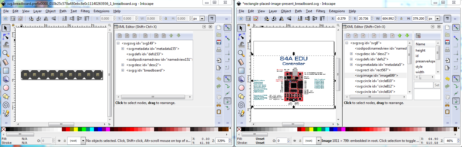
requested help to fix up a part. So while doing that I decided to record what I needed to do in order to fix the part to provide a tutorial to create new / fix broken parts. If you start from the Tarjeta S4A EDU.fzpz file posted in the above thread, you should be able to recreate my improved part posted in the same thread. I started by loading the original part in to Fritzing, that indicates breadboard is (at first look anyway) pretty good, but schematic and pcb are both broken (the image is red indicating missing connector definitions in both cases and the images do not match the board). Using 7zip I unzipped the Tarjeta S4A EDU.fzpz file which creates the following 5 files (a fzp file and 4 svg files one for each view):
part.S4A EDU_295a638d2eff112f7b0707b26a2df99f_12.fzp
svg.breadboard.S4A EDU_78c08539140e87873a7d0ebd198bd086_1_breadboard.svg
svg.icon.S4A EDU_78c08539140e87873a7d0ebd198bd086_1_icon.svg
svg.pcb.S4A EDU_78c08539140e87873a7d0ebd198bd086_1_pcb.svg
svg.schematic.S4A EDU_78c08539140e87873a7d0ebd198bd086_1_schematic.svg
If you haven’t already, configure your copy of Inkscape according to this howto:
as these settings are assumed in the following document. Due to the size of this howto (there is a size limit on forum posts, around 40,000 lines I think), I am going to split this in to one file for each view. Here I will start with breadboard view, then pcb view, then schematic view and fzp and completing and testing the part.
Since it initially seemed fine, I first rescaled the svg to be correct for Fritzing following the procedure here:
Then I did a google search to try and find documentation for the board. Turns out there isn’t much, I settled on https://www.gotronic.fr/pj2-34440-1407.pdf as the most usable document. There are no board dimensions, the only dimensions are for the 4 mounting holes at 25CM wide by 50CM high. The scale of the original svg is incorrect. The connectors (which should be on .1in boundaries) are 0.127in in x and 0.123in in y indicating the current svg isn’t a good indication of board dimensions. With that in mind I extracted the board image by importing the referenced pdf file in to Inkscape via File->import, then created 4 mounting holes (the same size as the holes in the image file) and positioned them so they are 25mm by 50mm apart. Then I reduced the width of the image file from the pdf via the width field in the Inkscape toolbar til the x coords of the mounting holes overlap the holes in the image like this.
pdf-mounting-holes-x-scaled-y-not_breadboard.svg.fzp (879.8 KB)
Note you need to remove the trailing .fzp because the forum has trouble with svg files but will accept a svg file called a fzp file just fine (and it turns back in to a svg file when you remove the trailing .fzp.)
Then doing y gives me a somewhat close image of the parts on the board (as close as we will get without better documentaiton) in this file:
pdf-mounting-holes-both_breadboard.svg.fzp (879.8 KB)
This is the basis for the new breadboard svg. For the connectors I am going to ignore the original breadboard svg (I ungrouped the scaled original breadboard svg and removed all the connectors to leave only the components in this svg):
orig-breadboard-without-connectors_breadboard.svg.fzp (56.9 KB)
Now I did Edit->select all then copy in the above svg and pasted the result in to the pdf-mounting-holes-both_breadboard.svg svg and then grouped the individual components (so they can be scaled by increasing/decreasing their height / width which will create transforms) which produces:
orig-svg-no-connectors-added_breadboard.svg.fzp (935.2 KB)
Then I scaled the various components from the original svg moving the component over top of the same component in the image and adjusting the w and h columns in the tool bar (working in px for macimumm resolution) so they overlap the component in the image exactly. If I had not had the original svg with appropriate components, I have a collection of various parts in breadboard view with the connectors removed that I could paste in to this svg. That is the easiest way to make a new breadboard svg from scratch. Now we need to deal with creating the underlying board that the components fit on. To do so use the rectangle tool on the left tool bar to create a rectangle in the drawing. Adjust its fill color using the color tool bar on the bottom of the Inkscape window to be about the same color as the board in the image. Select the rectangle and in the xml editor window click on the style entry. The style is currently
“fill:#c83737;stroke:#666666;stroke-width:13.20073414”
we need to change that to
“fill:#c83737;stroke:none;stroke-width:0”
to remove the border around the rectangle. Now use either the top tool bar or select and drag to make the rectangle the same height and width as the board in the image.
components-placed-image-present_breadboard.svg.fzp (935.9 KB)
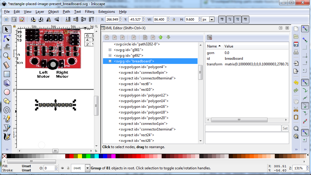
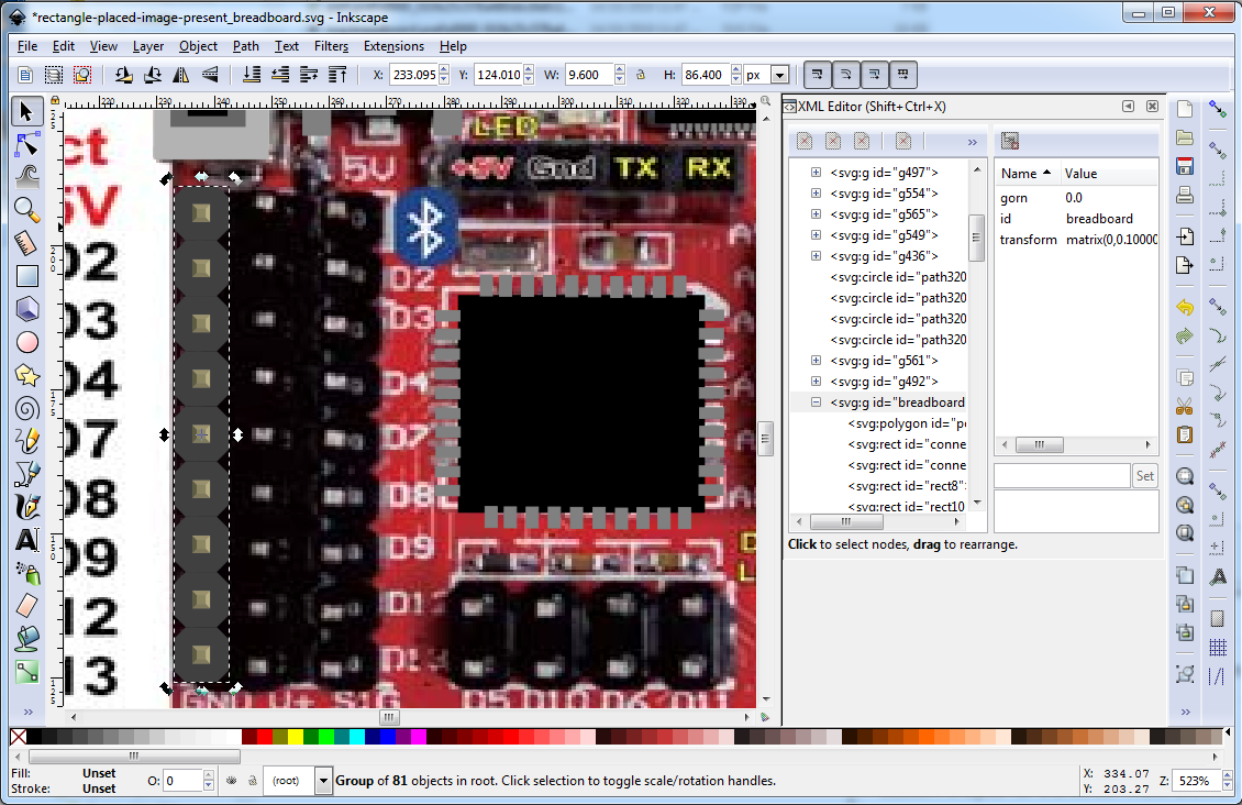
Now move the rectangle over til it covers the image. You will note that the rectangle covers all the components we placed. To fix that, click the move to top icon. If you don’t know where the move to top icon is, an image of it can be found in this document,
Configuring Inkscape for Fritzing
Click the move to top iconon the top tool bar to move the rectangle to the top of the xml display and allow the image and components to appear on top of it. As you see in this svg, the rectangle appears to have disappeared completely (that is because of the size of the image):
rectangle-placed-image-present_breadboard.svg.fzp (935.9 KB)
now if I delete the image we get this which is what (after we add connectors) the final board will look like:
rectangle-placed-image-removed_breadboard.svg.fzp (60.8 KB)
Now we are going to add the necessary connectors. We are doing that after the components that don’t have active connectors, so that we can cheat and let copy / paste do most of the work of defining the connectors for us. As all the connectors in this particular board are male headers of various sizes, I have a collection of generic male (and female) header parts that I exported from Frizting. I didn’t have a 9 pin male so start Fritzing, change to breadboard view (any of breadboard schematic or pcb will do) and drag in a generic header from core parts. Select the connector and use Inspector to set it to 9 pins male. Now right click on the part and select “Edit (new parts editor)” (note you want to be running 0.9.4 pre release or later. as it has a bug fix which will delete the parts when you exit parts editor which 0.9.3b does not). Without making any changes, select File->Save as new part. Click OK to the offered prefix value (we don’t care), to save the part to the mine parts bin. Close the parts editor and right click on the new part in the mine parts bin. Select export part and write the resulting fzpz file to your file system (remembering the name and location that the part is written to!). Exit Fritzing without saving (unless you have something else you want to save). Now go to the directory where you wrote the fzpz file and use an unzip program (I use 7zip which is cross platform) to unzip the .fzpz file. That will produce and fzp and 4 svg files. select the
svg.breadboard.filename_1_breadboard.svg
file and load it in Inkscape along side the svg file above (because we are going to copy / paste between svgs). You should have something that looks like this:
Now in the header Inkscape window click Edit-select all or highlight the breadboard group in xml editor then click Edit->copy. Now in the board breadboard window click paste and if the Inkscape gods are smiling on you you will get a new group called breadboard that looks like this:
If the Inkscape gods aren’t smiling on you (and for me they spend a lot of time rolling on the floor laughing, saying “we got him again”) you will get an image of the 9 pin header which is utterly useless. At that point I close Inkscape and copy preferences-install.xml to preferences.xml to reset it to the defaults so copy starts working correctly again. Assuming the Inkscape gods smiled on you and you have a 9 pin header as in the above image, the thing to note is the connector0pin and connector0terminal entries right below polygon4. This is the definition of a Fritzing pin, a few entries down you will find connector1pin and terminal. If you now duplicate (as opposed to doing the correctly lazy thing of copy / paste again), the pin and terminal ids will change to rect1234 the same as all the rest. While it is possible to figure out which ones they are and re type in connector0pin and connector0terminal, it is much easier to do the copy paste and not have to find the correct rectangles. Also of note is that at the bottom of the xml editor window you will see a transform (which is undesirable). Usually these will be removed when you ungroup the connector later (we want to be able to move it as a group right now though). Unfortunately that is not true if you rotate the part (which we need to do here), so in this case we will live with the transforms. As you will see in pcb, there we can’t live with transforms as they break gerber generation and we need to remove them which is very painful. In any case we now have our first connector ready to be placed so we need to rotate it by 90 degrees giving this:
Now repeat this for all the rest of the connectors 2pin 4pin and 6pin(creating them in Fritzing if you don’t already have them) until all the connectors in the image are covered by a copied in connector in a group. Once tht is done you can then delete the image leaving only the created components in the svg. At this point breadboard is almost done except for a bunch of tedious work. I’ve skipped forward a bit here, the next svg has all the connectors properly aligned and the pins numbering changed from the connector0pin-2 format to pin numbers starting at 0 and going up by one in a reasonable way down the board. This is a lot of work but not particularly difficult. You just select the pin in the svg then click on the connetcor0pin-3 label nearby, verify that is the pin you are intending to label and change the id in xml editor from connector0pin-2 to connector0pin and set it. There is one complication in that the first connector that you copy in will have its pins set as connector0pin (and up in sequence). If it is on fact not pin 0 (which is somewhat unlikely) then the first thing you need to do is find pin 0 (select any element in the xml editor window, press cntrl-f and enter connector0pin in the box that comes up will take you to the connector0pin element). You need to add a - to each pin in that one connector to hold the id fields (i.e. connector0pin changes to connector0pin- connector1pin changes to connector1-, etc.). The reason for this is that if that connector is not connector0, when you set the pin that is connector0pin Inkscape will replace the connector0pin id of the pin that has it to rect1234 (or such like) hiding the position of the pin. The single trailing - sign neither conflicts with any other copied in connector value nor with connector0pin anymore, leaving you with a connector id to change when that pins number comes up.
positioned-still-grouped_breadboard.svg.fzp (158.4 KB)
First we need to align the connectors to .1 in boundaries. To do that select a connector (I chose the outside 9 pin header on the left of the board which is connector0pin in the svg). Select that group by clicking on it and make sure the group (id breadboard in this case) is what is selected. With the tool bar set to inches, note the x and y coordinates showing in the tool bar (x 0.010 y 0.733 inches in this case). That establishes the base of the connector grid. All the rest of the connectors should start on X x.x10 and Y x.x33, so click on each connector in turn and use the tool bar to correct their position to reflect that. Usually boards are set so that the connectors are on the .1 grid (although there are exceptions most notably the Arduinos which have some of the connectors offset 0.5 in or there about). If you have positions for the connectors, use those values. Here I don’t have such information so I’m guessing they are on .1 boundaries. Hopefully the person that wanted this board will update the svgs using an actual board as the pattern if I am wrong. Next we need to copy the text from the image of the board in to the svg. I usually (as I did in this case) edit a breadboard file which has text and do a copy / paste of a string of text with the appropriate settings (a style like this: “font-size:49px;font-family:OCRA;fill:#ffffff”) and then change the text in the xml editor window to match what is needed. If you set the Inkscape tool bar to be in px (for maximum resolution) and position the added text in the middle of the pin as you will see in the finished breadboard svg, then change the tool bar dimensions to inches, you can click the up/down tabs beside the x and y indicators in the tool bar to position the text in x or y (which ever way it needs to go) in .1 in increments. Thus after placing the first text (the D2 label on the left side connectors) you can duplicate the D2, move it down one click (.1 in) in y and it will be in the correct place in x and y to have the text changed to D3. Again it is fairly simple (if work) to add and position all the rest of the required text. Once that is complete the part is almost ready to go. The only thing remaining is to remove all the groups we added for the components and the connectors. Doing this will remove most of the translates (unfortunately not all of them, but we will have to live with that). Once you have removed all the groups then click Edit->select all, then click Document Properties->Resize Page to content…->Resize page to drawing or selection to set the viewbox to match the outline of the part. When that is done with the select all still in effect either type cntrl-g or click Object>>group in the top tool bar to create a group of the entire part. When that completes (it may take some time for a large part), in xml editor select the id field of the group just created and set it to breadboard to set the appropriate layerId. Then File->save as and select plain svg from the bottom menu and change the name of the svg file from save the part. Now breadboard is finished and saved. It should look like this:
svg.breadboard.S4A_EDU_1_breadboard.svg.fzp (180.5 KB)
On to pcb. In the original, pcb doesn’t look anything like the board (it is likely left over from the part the original was cloned from). Thus I copied the above breadboard file over the pcb files since the pin positioning will be the same (although the pads will be different). To create the svg below I opened both the newly copied breadboard which is now pcb svg and the pcb view of the generic 9 pin header that I created from Fritzing earlier. In the 9 pin header pcb svg, I selected the copper0 group (to get a single group with the appropriate pads below in) and did a Edit->copy. Then in the pcb svg I did an Edit->paste and moved the resulting 9 pads near to the actual connector. I then copied in a line (because Inkscape won’t generate a line, but will deal with them for compatability with Illustrator which does generate lines). I set the style of the line to be “fill:none;stroke:#000000;stroke-width:10;stroke-linecap:butt” to create a line suitable for silkscreen (black and 10 thou in wide) and (after making sure “scale stroke-width” was disabled again, so extending the line does not change the stroke width) positioned and sized the lines to go around the edge of the board in breadboard and cover the USB connector on the top of the board. As well I created 4 circles and placed them on top of the 4 mounting holes to complete the silkscreen. That produces this svg:
header-copper-present-not-placed-pcb.svg.fzp (184.2 KB)
silkscreen is complete in its final form, all the remains is to correctly position the connectors. If we had measurements of the actual board we would use those to position the connectors, since we do not have measurements I again picked a position for the left most 9 pin header, and then copied the appropriate still grouped size of connector from the pcb svg of the appropriate size male header. That gives us an svg that looks like this:
placed-but-not-aligned_breadboard.svg.fzp (158.4 KB)
Now set the tool bar unit to inches. Use the left most 9 position header as the reference point so record its x y coords in inches, so select copper0 (the grouped left most 9 pin header) its x coord is 0.020in and its y coord is 0.745in (at the bottom of the connector. to make all the other pins aligned ae they should be adjust their x and y coords to match the form n.n20 in for x and n.n745 in for y, where n.n are digits from 0 to 9. The battery connector at the top does not appear to be aligned on the .1 grid like the rest of the connectors so I left it alone. Once that was done the group breadboard was selected and deleted to remove the breadboard image from pcb, Now we can ungroup all of the groups in pcb. Once that is done, start at connector0pin and set the id of each connector in xml editor to match breadboard (the pads are obvious here so we don’t need to be careful about not overwriting pin numbers already in use). If the 4 circles and 6 lines that make up the silkscreen are not already at the top of the xml editor window, move them there. Then starting with connector0pin, move the connectors one at a time to the bottom of the xml editor window (there is an icon on the tool bar to do this). The end result should be the connectors in in creasing order at the bottom of the xml window. I didn’t do this in breadboard because if you do some of the pins will disappear as the display elements in the headers occlude one another. In pcb and schematic that isn’t a problem and it is preferable to have all the connectors at the bottom in order to make finding connectors easy. You should end up with a svg that looks like this:
pads-in-place-ungrouped_pcb.svg.fzp (14.5 KB)
At this point it is good practice to edit the svg with a text editor (I use vi under cygwin on windows, but any text editor that can search should do). Search for rx which indicates an ellipse rather than a circle. If it is a connectorxpin pad you need to change it to a circle by setting both rx and ry to the same value via xml editor. Then do a search for tran (for translate). If you have translates you need to remove them as they will break gerber processing. In this case we indeed have translates in the 4 pin headers that had to be rotated 90 degrees to align with the direction of the connectors on the board. Removing the group did not remove the translate (I don’t know why). Since I forgot to keep this particular svg variant I replaced the top 4 position connector with a grouped and rotated one then ungouped it to make this demonstration svg (which in fact works fine with the translates in place, again I don’t know why because the original did not!):
4-pos-transform-rotate_pcb.svg.fzp (14.2 KB)
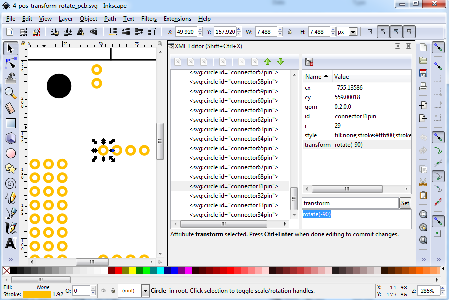
While I have been unable to reproduce this problem to demonstrate it here, it is still best practice to remove translates everywhere possible (they are a performance drain, although it is unclear how serious a drain at present) because they imply a floating point matrix multiplication at every render (and Fritzing renders a lot). Thus I will now remove the transforms. This indicates the problem:
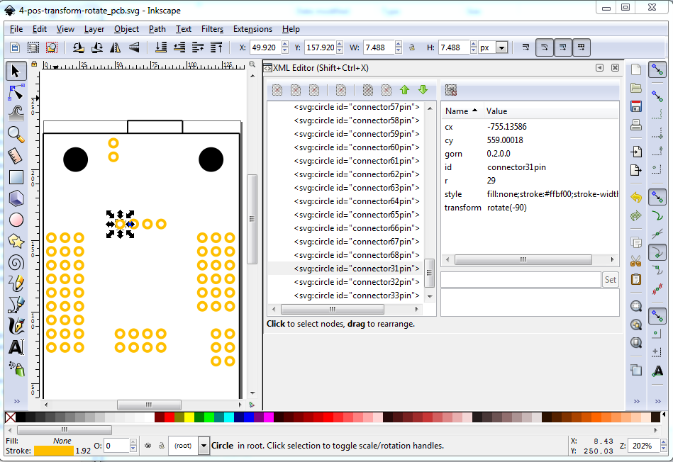
as we see there is a transform rotate(-90) in the xml for connector31pin (and 32, 33, and 34 below it). Removal is fairly simple if time consuming. First record the x y coords of the translated pad. In this case x 49.920 px y 157.920px. Now select the translate in xml editor, delete the rotate(-90) (leaving the bottom window blank) and press set. The pad disappears, and the tool bar now says x -76.237 y 176.749. What has happened is the pad has moved outside the view box (which causes the gerber code to not display it because it is outside the view box in the gerber codes view of things). The easy thing would be to use the Inkscape extension Apply Transform which is supposed to collapse transforms where possible (some transforms dealing with stroke-widths and possibly other constructs, can only be done at render time, not precomputed.) When applied to this (even with the svg ungrouped which should be the easist case) Apply Transform makes the transform more complex which isn’t useful. It also tends to sometimes toss a python exception during processing, with the result I more or less ignore it now. The test against this file is the first time I’ve tried it in a couple of years. So we have to do this the tedious manual method which because it works indicates this could be automated if someone knew how and was willing to put in the work. My long term goal is to make FritzingFixPart.py remove what transforms it can,but that is likely a long way off. This image, in the xml editor window shows the undesirable transform(rotate 90). Inkscape could have (and in my view should have for perfromance reasons) removed this transfrom by altering the coordinates to remove it as we are about to do manually, but it doesen’t.Here the transform has been removed by selecting the transform rotate(90) in xml editor like this:
and then pressing set which has the effect of removing the transform (and changing the drawing to reflect the removal of the transform) which results in this:
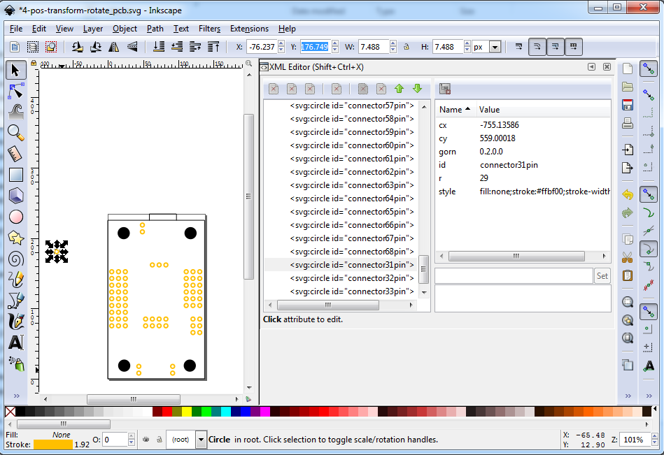
Note that the pad that was highlighted has moved off to the left out of the viewbox (where it will be truncated by Fritzing because it is outside the viewbox). To fix this, we set the tool bar x y coords back to the orignal values which will move the pad to its orignal position without the transform like this:
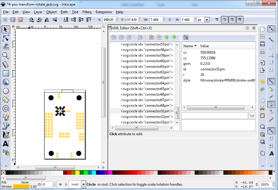
Now repeat this for the other 3 pins in this connector and the other 2 4 pin connectors. If anyone knows of a way to get Inkscape to remove the transforms I would love to hear of it. Now Edit->Select all, Document Properites->Resize page to content->Resize page to drawing or selection to reset the view box correctly. Now select all the copper pads (and unfortunately the 4 mounting holes intended to be part of silkscreen) and group them
then in xml editor select circle1487 and click unindent node (the icon circled in red here):
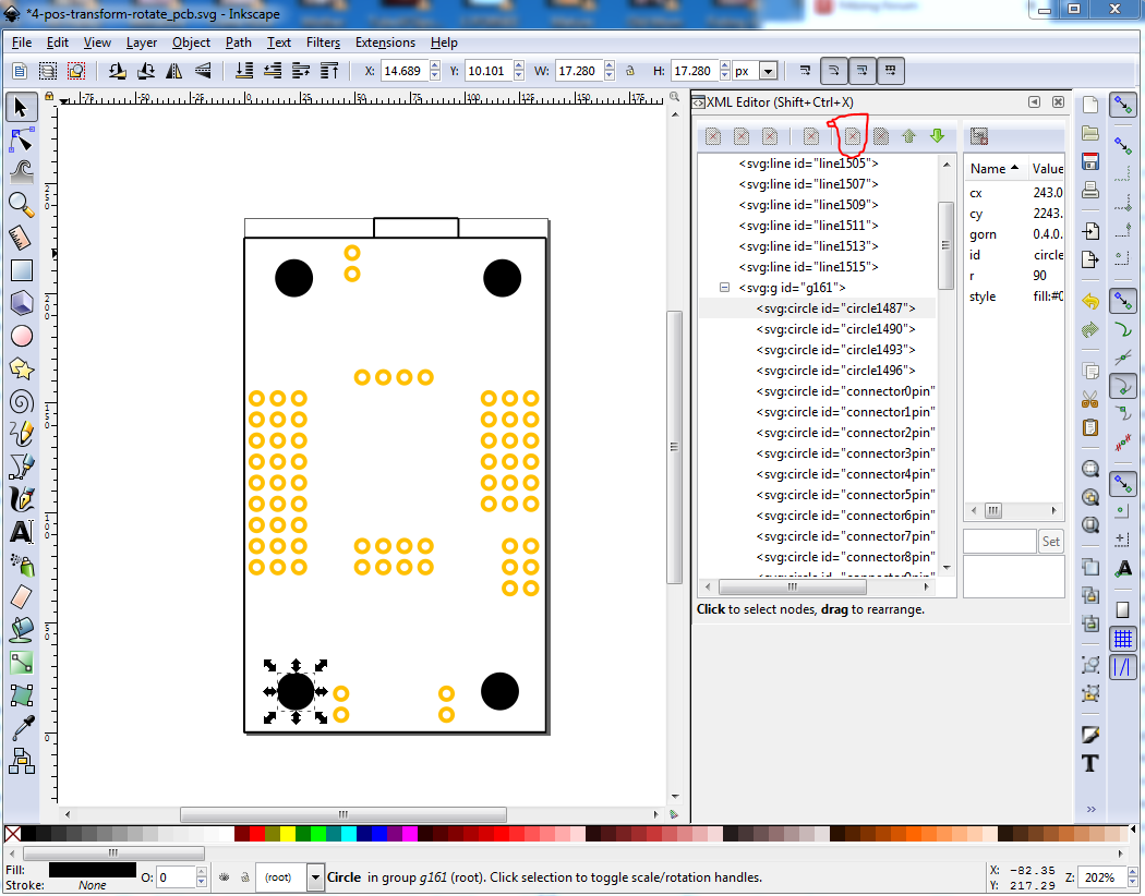
which changes to:
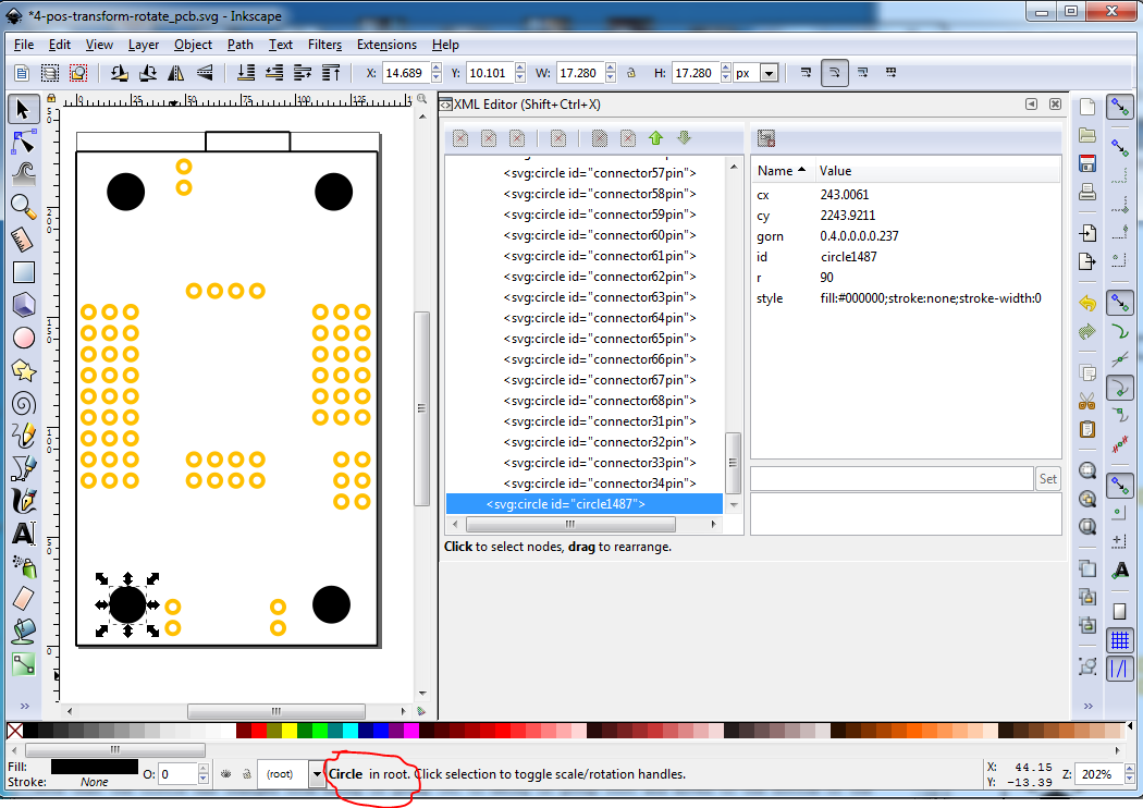
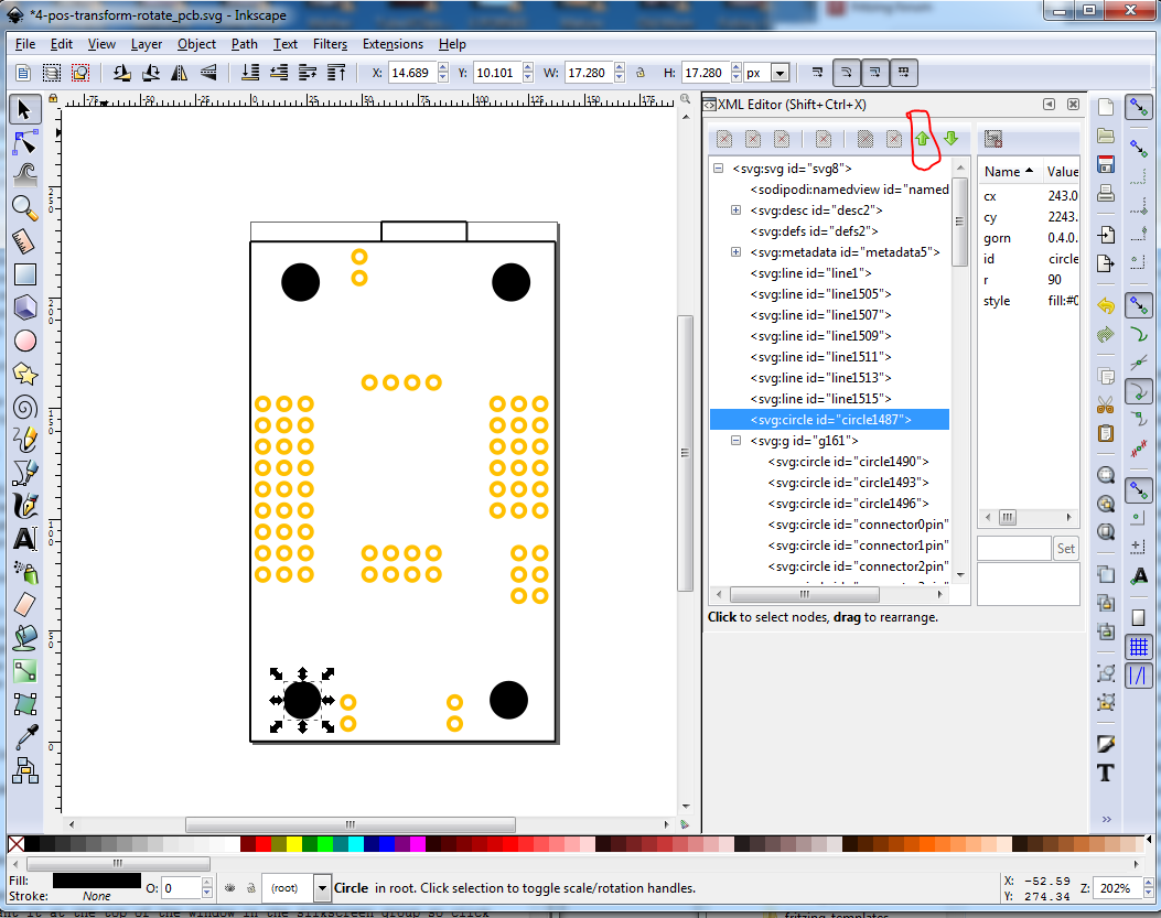
note that the circle has changed from being in group 161 to being in group root (outlined in red on the bottom of the screen) and moved to the bottom of the xml window. We want it at the top of the window in the silkscreen group so click the up arrow beside the indent node icon in xml editor and it will move there (the correct icon is circled in red in this image):
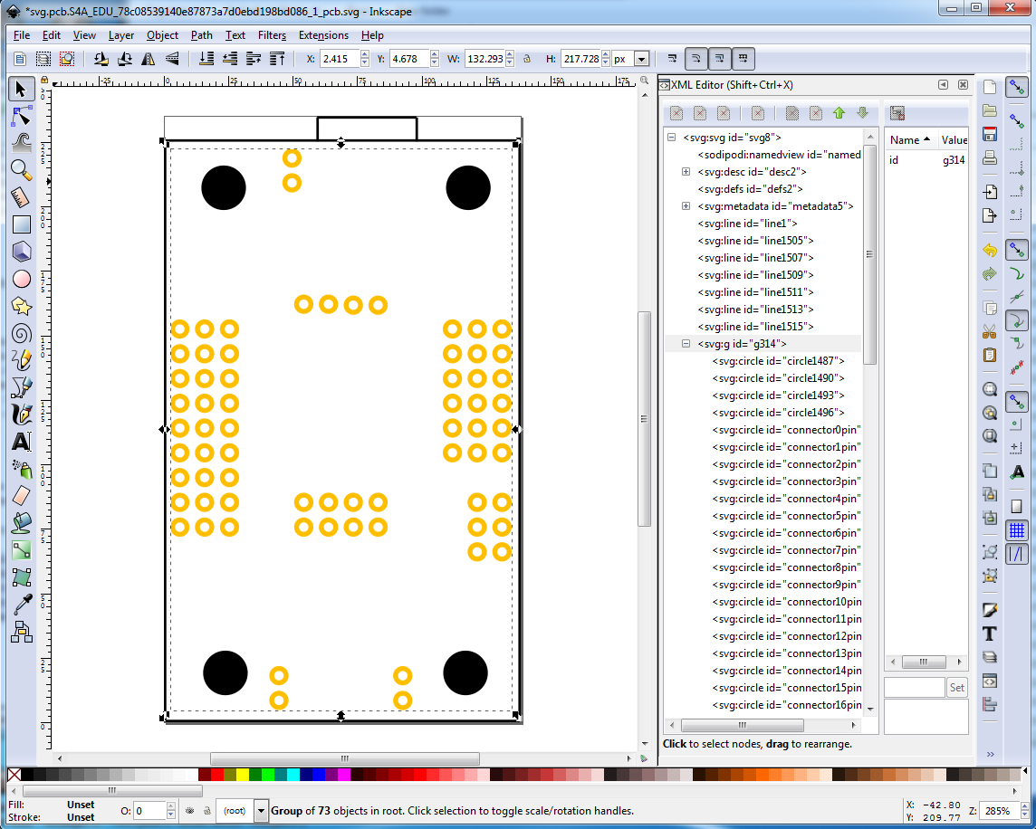
Now select circle1490, unident node and raise node, select circle1493, unident node and raise node, select circle1493, unident node and raise node, select circle1496, unident node and raise node. Select the new group and group it again. Change the id of the top group to copper1 and the next group down to copper0. Do Edit->select all, then object->group, then change the id of the new group to silkscreen. Select group copper1 and unindent node to move it back in to group root. Now File->Save As, set tye to plain svg and save to save the finished pcb svg file which should look like
svg.pcb.S4A_EDU_1_pcb.svg.fzp (15.4 KB)
Now we need to do the schematic svg and fzp, that will be done in part 2 of the post here: