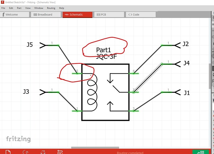
Welcome aboard! Your part has a few problems.
In general you need to be obeying the under the CC 4.0 BY-SA, rules in this case that probably means a line like this as author in the fzp file
author>Robert Oostenveld, Stéphane Passignat (modified by vanepp May 2021)</author>
where you leave the original authors in place but add a modified by line to indicate that you made the changes (although I am far from an expert on what is required under CC by SA.) That said on to the problems in your part. You are missing terminalIds and a label field
That causes the part to be misaligned in schematic and the wire to connect to the middle of the pin (and misaligns the part to the grid) The label field should probably be RY for relay rather than the default “part”. As well FritzingCheckPart.py has a number of complaints:
Warning 14: File
‘part.jqc-3f_1_49e7ea04fd9380c72da0adc8f0313d20_10.fzp.bak’
At line 48
terminalId missing in schematicView (likely an error)
Warning 19: File
‘svg.breadboard.jqc-3f_1_058681f3473df29594542efc29edc9a6_1_breadboard.svg.bak’
At line 3
Height 54.212597 is defined in px
in or mm is a better option (px can cause scaling problems!)
Error 18: File
‘part.jqc-3f_1_49e7ea04fd9380c72da0adc8f0313d20_10.fzp.bak’
Connector connector3terminal is in the fzp file but not the svg file. (typo?)
svg svg.breadboard.jqc-3f_1_058681f3473df29594542efc29edc9a6_1_breadboard.svg.bak
Error 69: File
‘svg.pcb.jqc-3f_1_058681f3473df29594542efc29edc9a6_1_pcb.svg.bak’
At line 17
Found a drawing element before a layerId (or no layerId)
are a few of them. This tutorial may help with correcting these errors
Your pcb svg lacks a silkscreen layerId and is in an old format (separate copper0 and copper1 it looks like hard to tell because of all the groups!) Hope this helps!
Peter
