"Show in Folder" doesn't show

Hello, I’m trying to locate .svg file locations with File > Show in Folder from the new parts editor in Fritzing 0.9.4 64 bit running in Windows 7 Pro. Explore will always pop up but only once in a great while will it actually locate (highlight) the .svg file.
The majority of the time explore comes up with “C:\Users\user\Documents” instead of “C:\Users\user\Documents\Fritzing\parts\svg\user\breadboard” where my (user) .svg files are actually located … non user files are what I’m mostly wanting to find though.
Got File > Show in Folder to find an .svg file correctly once or twice but can’t for the life of me duplicate how I did it.
Please Help

Welcome aboard! I’m not really sure what you are trying to do, I expect make or modify a new part, (and I rarely use Parts Editor as well.) As far as I can see the show in folder option is to find the location of the svg for the currently edited part. In this example I ran Parts Editor against a resistor (a bad choice, because it has bendable legs which PE does not support!), then Clicked File->Show in folder.

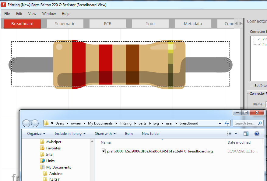
That correctly tells me the breadboard svg for the resistor is in

C:\Users\owner\Documents\Fritzing\parts\svg\user\breadboard\prefix0000_f2e32000cd10e3da86673451b1ac2ef4_0_breadboard.svg

which is where parts editor has stored the svg it is working on. That will probably be erased when parts editor is closed (assuming I don’t save the part), so is likely not a good choice to edit. although I expect you could edit that location with an svg editor such as Inkscape and change the svg successfully. What I usually do is click File->save as new part then OK to the prefix (changing it from prefix0000 if I want or leaving it, doesn’t matter.) That writes the complete part in to the mine parts bin (the top right on the Fritzing window. From there right clicking on the part in the mine parts bin and selecting Export part will write the part as a .fzpz file in the file system. If you then unzip (I use 7zip) the fzpz file you will get the fzp file and the 4 svg files for the part. I usually ignore parts editor and edit the files directly but you can use an svg editor to modify the svg files then load the part in parts editor again and use File->Load image for view to load your modified svg file in to parts editor. If you are trying to create a new part, then these two tutorials may help:

both apply to the latesf Fritzing release, most others are for older versions. Asking for help here is unfortunately the best way to learn to make parts so far.

Peter

Thank you for your quick response and also for your very detailed “Parts creation howtos” which I have already started getting into. As far as the question I posted, I repeated your example of the 220 ohm resistor in Parts Editor and Clicked File->Show in folder. The location or path I got was still the same as I explained earlier: “C:\Users\user\Documents” with no svg file indicated. So, I used part of the path you came up with and searched for it manually. What I found was “C:\Program Files (x86)\fritzing\fritzing.0.9.4.64.pc\fritzing-parts\svg\core\breadboard\resistor_220.svg” I opened it in Inkscape and it appeared to be the same as what’s shown in fritzing.
Your path has “\user” in it so I assume you saved the resistor to your “Mine” parts at some point. I too had saved that resistor to “Mine” parts but there was no svg of it in my \user\ path.
I still have an older version of fritzing on my PC and the resistor svg is located at “C:\Program Files (x86)\fritzing\fritzing.0.9.3b.32.pc\fritzing-parts\svg\core\breadboard\resistor_220.svg”. Could the fact that I have two versions of fritzing be causing File->Show in folder to fail at “C:\Users\user\Documents”?

Yes, unless you do something (usually a source code change although there are rumors of a command line switch as well although I don’t know it) Fritzing will save the various user files in (on Windows):

c:\users\username\AppData\Fritzing\roaming\Fritzing (which is a hidden directory so you need to enable hidden directories in explorer) and

c:\Users\username\My Documents\Fritzing (where username is your windows id)

by default the path will be the same on both versions, and if you change between them the user files are likely to get corrupted as the new version over writes some of the old versions files and probably gets different values from other fields. When I’m running development versions compiled from source. I change the hard coded path so the two versions use different user directories. Renaming the 2 directories (to something like filename.version) when changing versions (you need to rename the appropriate filename.version back to filename or Fritzing will create and populate a new set.) will also work as long as you remember to do it when switching versions (a batch file that does it automatically would probably be safest). Your mine parts bin is one of the things that is stored in the user directories.

Peter

On your suggestion, I attempted to change some of fritzing’s paths like can be done in other programs. Edit->Preferences seems to be the only way to make changes to fritzing but unfortunately, I couldn’t find any tab that led to a way to edit paths.
The good news is, by fiddling around, I found a sequence (if you will) that seems to work every time! … probably a no brainer for most users.

  1. run fritzing
  2. select breadboard tab
  3. left click and drag a part onto the Breadboard
  4. right click on the part ON THE BREADBOARD NOT THE ONE IN THE PARTS BIN
  5. select Edit (new parts editor)
  6. after it opens, select Show in Folder from the File dropdown menu

And here is what I correctly get every time:
C:\Users\user\Documents\Fritzing\parts\svg\user\breadboard\prefix0000_27f3d47e9c6791f4fec53d53d9af1147_0_breadboard.svg
My mistake was right clicking on parts in the parts bin and running the parts editor from there … the part opens up but File->Show in Folder will not locate the svg.

I do have a question about a comment you made earlier in which you don’t use fritzing’s parts edit much so is there another way to assign pins to graphics other than the parts editor? (you probably answer that in your “Parts creation howtos”, I just haven’t gotten that far yet)
Thanks Again Sky

Actually this strikes me as a bug (or at least an enhancement request.) The rule of least astonishment (which Fritzing tries to obey) indicates that Parts Editor should act the same no matter where you start from. I’ll make a test case and file a bug report. I’ve run Parts editor from the parts bins lots, but I usually just do save as a new part and export it, and so have never noticed this behavour.

I’m thinking a new (maybe part 0) section of the howto that details the layout and relation ships of the .fzp and 4 svg files may be useful to make this clear. The parts editor is editing both the fzp file and the svg file to associate a pin to a graphic. I believe (but could be wrong) that the connectors must be defined in the fzp file for parts editor to be able to associate them, I don’t think it can add new connectors. It starts in the .fzp file (which defines the entire part) in the connectors section:

 <connectors>
   <connector id="connector0" type="male" name="">
     <description></description>
     <views>
       <breadboardView>
         <p svgId="connector0pin" layer="breadboard"/>
       </breadboardView>
       <schematicView>
         <p svgId="connector0pin" layer="schematic" terminalId="connector0terminal"/>
       </schematicView>
       <pcbView>
         <p svgId="connector0pin" layer="copper0"/>
         <p svgId="connector0pin" layer="copper1"/>
       </pcbView>
     </views>
   </connector>
 </connectors>

Here each view has a definition of the pins in that view, in the breadboard case we only have connector0pin and the wire will connect to the center of the pin which is usually what we want in breadboard. In the case where we have a pin (like in schematic below), you can add a terminalId definition and a connectorxterminal and it will function the same as schematic. In schematic we have both connector0pin and connector0terminal because in the svg the pin is a line .1in long and the terminal is a 10thou by 10thou square. If the terminalId is omitted, the wire will connect to the center of the pin (which is usually not what we want). In the schematic svg the xml looks like this:

  <line
    x1="4709.2393"
    x2="4804.1816"
    y1="605.17145"
    y2="605.17145"
    id="connector0pin"
    fill="none"
    stroke="#555555"
    stroke-width="10"
    stroke-linecap="round"
  />
  <rect
    x="4800.0015"
    id="connector0terminal"
    y="600.37628"
    width="10"
    height="10"
    fill="none"
    stroke-width="0"
  />

In Inkscape it looks like this:

The line (if there is no terminalId the wire will terminate at the arrow circled in red)

and the terminalId:

with this present the wire will terminate in the center of the square and thus at the end of the terminal. Parts editor adds the terminalId to the svg if it is not present and moves it to one of center, e, w, n, s for the 5 possible positions you might want the terminalId to be in. I find it easier to use Inkscape to place the teminalId where I want it, but both ways will cause the same effect (except I can rarely get Parts editor to set the positions for some reason :slight_smile: .) While modifying the xml looks (and is!) complex, once you are used to it it is fairly easy to do. In order to write the part checking script I had to figure out what all the xml does, so for me this is the easy way now.

Peter

Hmmm, not sure how you got to the code in the .fzp file but I do recognize the XML editor from Inkscape. Both codes remind me of scripting but I’m so used to pointing and clicking … well I’m glad there’s more than on way to do it!
If you decide to do a part 0 in your howtos, please keep me informed. There are several things I believe would have helped me if I had understood the basic concepts early on. One item is layers. Many other programs use layers; you can name them, color them, assign objects to them, etc but when I run Inkscape on an .svg and pull up the layers menu, there are none?? and layers are often referred to in explanations.
In my fiddling around, I pulled up a part in the Parts Editor and clicked on some of the pads to see how their pins were set up in the Connector list on the right. Some would jump to a pin on the right and some wouldn’t. When hovering over a pin that I wanted to select, something (often a big block) would prevent me from selecting the pin. Is this the concept of layers in fritzing? I did recall from something I read that the XML list in Inkscape is ordered from bottom to top so I loaded the part’s svg into Inkscape, moved all the pads in the editor to the bottom, saved it and tried again. Sure enough, all the pins were now clickable.
I’m going to keep hanging in there so that one day, with help from good people like yourself, I can finish the A-Star board from Pololu and use it in fritzing.
Sky

That is fairly easy, I just unzipped (using 7zip) the .fzpz file, that unpacks the .fzp and the 3 or 4 svg files that make up the part. I typically edit the files (text editor for the .fzp and Inkscape for the svgs) then rezip them in to a .fzpz file.

I don’t know much about layers (the only svg editing I’ve done has been for Fritzing) so my usual starting position is ungroup everything which I think eliminates all the layers. Fritzing tries to tolerate most anything, but it is perfectly happy (AFAIK anyway) with no layers and the whole svg as a single group with the id set to the layer name (such as breadboard) so I try and stick to that. As you will see for parts editor svgs, parts editor loves groups and will nest them (needlessly as far as I can see) very deeply. There could be something useful this does that I don’t know about though.

Unfortunately I don’t know, I have seen the references to layers in the documentation at times, but I don’t know what they mean (and I don’t think there is anyone left posting that does although I’d welcome being proven wrong!) I think the select mechanism in Fritzing does indeed work from bottom to top. That is certainly true in pcb, where is silkscreen is the bottom group with copper1/copper0 above it, then when you select in pcb view it will prefer the silkscreen rather than the traces which is rarely what you want. That is why the check script issues a warning if Silkscreen is after the copper layers. I would assume the same is true for parts editor (that may be the source of my problems with parts editor in fact.)

Feel free to post the .fzpz file (even if it has problems), often the easiest way forward is for one of us to point out what is wrong (sometimes finding new errors to add to the parts checking script on the way by :slight_smile: .)

Peter

Given what @vanepp wrote, I should do a more detailed write up. I had not realized there would be confusion around this. My background said it was obvious.

Layer is a generic term. It just means (conceptually) things that are grouped/packaged together, and can be stacked over/under things on other layers. Multiple transparencies stacked up, each with different things drawn on them. Technically, in some contexts, z ordering (what is above and below a single item) can be independent of layering, but the way Fritzing uses it, everything on (in) a single layer will always be above or below anything on a different layer.

I suspect that (for Fritzing) the term was brought in because of the layers of a pcb. Fritzing only uses top and bottom copper layers, but pcbs can be created with a lot more. Plus the silkscreen as another layer “over” the outermost copper layers. With that as a base, it was expanded (for code reuse) to the similar concepts for the other views. Even though the other views only have one layer each (the way Fritzing defines them). The above was based on the way parts are defined, but exactly the same applies to parts in sketches. Additional layers could have been used in sketches to help manage groups of breadboard z ordering, but explicit number ranges were used instead.

In the part (fzp) file, which is an xml file, Fritzing needs a definition of what layers are to be used for each view. (normally) everything except pcb view uses only a single layer for the whole view. The Fritzing/view layer is identified (and defined) by a ‘layerId’ in the fzp file. The value of that id needs to match an ‘id’ attribute (for a g (group) element in the referenced (for that view) svg file. Which is also based on xml. That id value/name may or may not correspond to any particular svg editor tool’s concept of what a layer is.

So a Fritzing layer is the named group (and all of its content) in the matching view image. For pcb, that “and all of its content” is important, because THT devices normally have 2 copper layers, with one created inside of the other. By putting all of the common content (copper pads) inside the 2nd (inner) copper layer (group) in the svg image file, the content exists in both Fritzing layers.

The view svg image files can contain content (graphics) that is not part of the specified layer(s). That content will normally be invisible, but in some situations Fritzing will still process and use the information. That can be done for things like the graphics to provide a snap point for the end of connector pins. Something has to exist (with another id value) to let Fritzing identify where the desired end is, but no graphics needs to be shown for it. Keeping the terminal point graphics outside of the layer (group) does that.

And yes, the typical use for svg image content, is that the things at the beginning of the file are below anything that comes after. The later “covers up” what came before, so the last thing, at a specific coordinate, is going to be the first thing seen when clicking. By default. The code could change that, and as mentioned should for silkscreen, at least in a sketch. I have not noticed selecting silkscreen content there, so maybe you (@vanepp) meant that only for parts editor? (which I do not use, and where sometimes selecting silkscreen might useful. If parts editor has the same view controls as the sketch, just turn off silkscreen when want to ignore it. Which is what I do in a sketch file, to hide the ratsnest lines, and opposite side copper, to make it easier to grab the wire/trace I really want.

Hopefully that helps, and does not just add to the confusion.