Probably a look at this tutorial series will help:
I rarely use parts editor, preferring to edit the files directly. A .fzpz file is really a zip file. You can use 7zip (an open source unzip) or probably any zip program to unzip a .fzpz file. That will give you a .fzp file and 3 or 4 (depending on whether there is an icon svg) svg files in a format like this:
LIDARLite-Fritzing-Part-improved-more.fzpz
part.LIDAR-Lite_9e97bcd3cf44a322803ec9abc8070459_1.fzp
svg.breadboard.LIDAR-Lite_a79a4859e8e63cf63a1e0013a141f8ef_1_breadboard.svg
svg.pcb.LIDAR-Lite_a79a4859e8e63cf63a1e0013a141f8ef_1_pcb.svg
svg.schematic.LIDAR-Lite_a79a4859e8e63cf63a1e0013a141f8ef_1_schematic.svg
where
LIDARLite-Fritzing-Part-improved-more.fzpz
contains the .fzp and 3 (in this case no icon, as I reused breadboard) svg files. The funny part. and svg. prefixes are for the Fritzing loader who will store them in a series of directories like this (which is the format of the parts git repository):
core/
fzp-file.fzp (stripped of the part.)
svg/core/breadboard/
file-breadboard.svg (stripped of the leading svg.breadboard)
svg/core/pcb/
pcb.svg
svg/core/schematic/
schematic.svg
When you have done the editing, just rezip the fzp and the 3 svgs and rename the .zip file to .fzpz and Fritzing will happily load your changes. For the tube socket I’m fairly sure I can duplicate lines then use transform/rotate in Inkscape to get the angles, then add half the length of the line in X to center the rotated lines on the bounding circle. It will be fun to try, and I’ll document it for others assuming it works as I expect.
Edit:
That was easier than I expected. Here is a part, hopefully correct ![]() the holes are 0.07in in diameter the pins show as 1.7mm which is 0.066in so hopefully enough clearance, but the hole may need to be a bit bigger to fit properly.
the holes are 0.07in in diameter the pins show as 1.7mm which is 0.066in so hopefully enough clearance, but the hole may need to be a bit bigger to fit properly.
tube-socket-7pin.fzpz (3.8 KB)
and an explanation of what I did:
Start with 9pin pcb svg
ungroup
reduce circle diameter to 18.6mm via dia to get radius then restore the diameter and change the radius to change the size of the circle without moving the center point (which changing the diameter does.)
duplicate the circle to make the pin circle at 9.5mm reduce the stroke width to 1 before resetting the radius (again set the diameter in the toolbar to get the proper radius, then back out the change and change the radius in xml editor.)
maka a stroke width 1 line 9.5mm long centered in the circle then duplicate it.
set y to the y value of the circle then adjust x til the line is in the center of the circle.
duplicate the line, then object->transform->rotate 45 degrees and apply.
dup the resulting line and rotate it 45 degrees
dup the resulting line and rotate it 45 degrees
We now have the points where the pads should be on the circle so move them in to position.
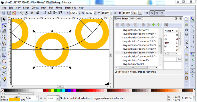
copy in a line twice, rotate one 90 degrees and line them both up to intersect the 45 degree line on the circle. Then adjust the x/y position of connector0pin to be on the lines.
holes of 0.07in reduce stroke-width to 20 so diam .11in radius 45
Below (forum willing ![]() ) is the pcb svg with the construction lines in place:
) is the pcb svg with the construction lines in place:
The forum (with the usual edit the px values to go from 1 to 1000px) was willing, so if you right click and “Save image as” on the svg above you should get the svg with the construction lines described above still in place. If you select connector5pin, you will see how the construction lines are used to position the pads.:
On the 9pin socket, the pad size was 40 thou in, in this one that was reduced to 20thou because 40 thou overlaps and shorts.
Peter
