Ah! I saw the package and pick and place drawings and stopped reading in the pdf. Indeed the needed information is there. I see that all the pins in the pdf are the same length, in the other image notice that the end pin is shorter (likely the power pin to allow hot swapping which you may not need but it would be best to check!) That may cause a problem if they need the pins to all be shorted together for plating though. I haven’t done a gold plated edge connector board in 40 years or more, so the other thing to check with the board house is if they still need all the pins on the edge connectors shorted together by a trace that will be truncated like this
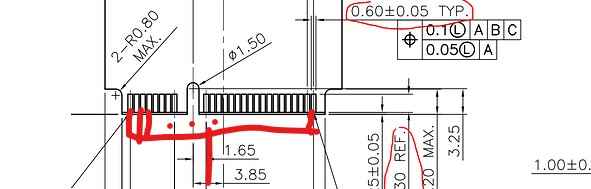
the red lines on the bottom connect to each pin so the pins all connect together to allow gold plating via electoplating. After that the board is truncated to the bottom of the edge connector to isolate the now plated pins. It would be wise to check if this is still expected / needed these days. It is possible they can just dip the pins in a solution and plate them these days and no longer need the short. As well edge connectors in Fritzing are a special odd case that requires separate copper1 and copper0 layers (which is supported by Fritzing but not by parts editor) so you need to be comfortable with directly editing the svg and fzp file to make this board Parts editor won’t work for it. This tutorial set may have the edge connector layout in it (I don’t remember at this point) but is in any case what you need to be comfortable doing to make this board.
looks like edge connectors are here instead
Peter