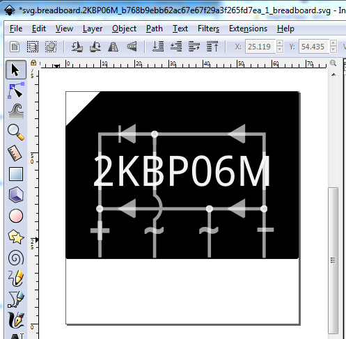
Welcome aboard! People willing and able to make parts are especially welcome. Your part is fully functional as it stands while it can be improved in a few places it should work fine as is for most uses. The layerIds in most svgs were wrong. The only thing that does is cause the part to not be exported in a svg or pdf though. Breadboard has a copy of schematic (which I removed) embedded in it but not visible (although it will be rendered every time):
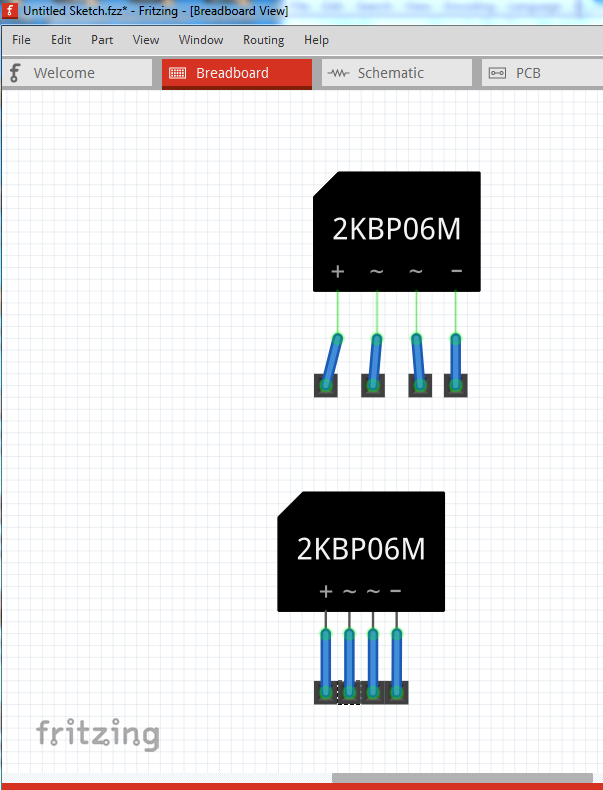
As well the pins are spaced .15in apart (as they are on the real part), where we usually reduce them (as I have done here) to .1 in to fit on breadboard correctly. This is a judgement call, sometimes parts are shown as they exist in real life (because the intent is to make them like real life!) I also made the pins wider (and probably should have made them wider yet) to be more visible in breadboard.
pcb
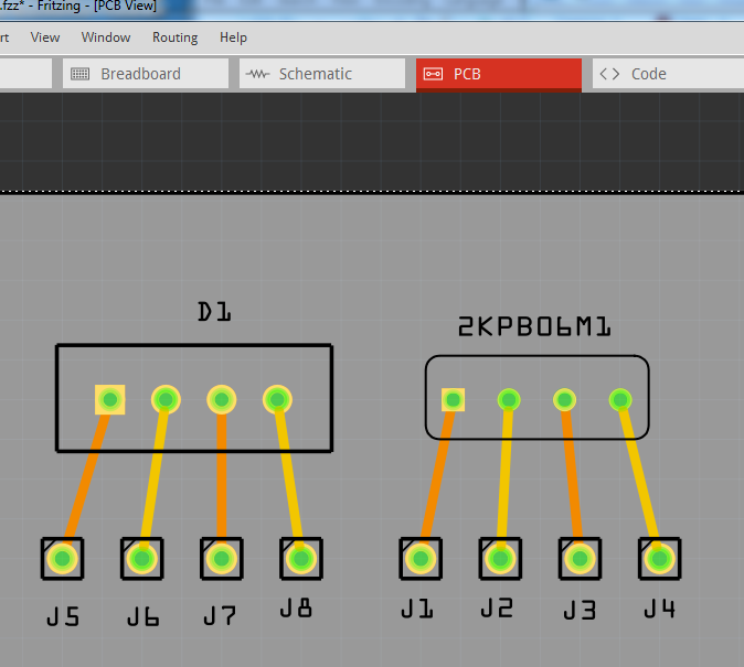
I removed the path for the silkscreen and replaced it with 4 lines that outline the package (you path appears a little small compared to the data sheet) and increased the size of the pad surround from 10thou to the standard 20thou and the hole size from 0.033in to a standard 0.035 IC hole.
schematic
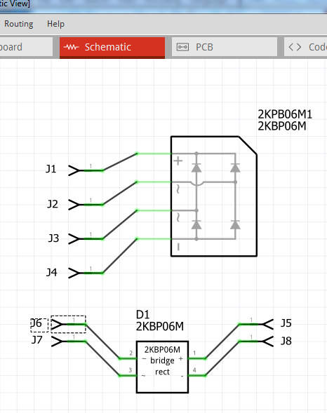
I replaced entirely to make the inputs (the ac) on the lefr and the outputs on the right and reduce the size. Space in schematic is valuable, and so the smaller the better. We also like to keep the pins on .1 pitch (again to reduce space and match other parts.) I note that you got the terminalId correct (without a terminalId the wire will connect in the middle of the pin which looks ugly!)
finally the fixed up part (with a new moduleId so it will load beside your part for comparison) and the test sketch the above screen shots are from:
Bridge-Rectifier-600V-fixed.fzpz (4.9 KB)
test-Sketch.fzz (22.7 KB)
and finally pointers to the two sets of parts making tutorials that apply to the latest version of fritzing (most of the others are for older versions):
If you find things that are unclear feel free to ask!
Peter