Your part has a number of problems. This tutorial may help with curing them:
The first thing I did was run FritzingCheckPart.py against the part to check its integrity. Here is an edit for size summary of its output (it is very verbose.!)
$ FritzingCheckPartw.py part.PCM1808_39018436c7a78322bff523fa2b4808bb_1.fzp
**** Starting to process file Startup, no file yet
**** Starting to process file part.PCM1808_39018436c7a78322bff523fa2b4808bb_1.fzp
**** Starting to process file svg.breadboard.PCM1808_f5262701827fb87fd599debbd98f8df9_2_breadboard.svg.bak
**** Starting to process file svg.schematic.PCM1808_f5262701827fb87fd599debbd98f8df9_2_schematic.svg.bak
**** Starting to process file svg.pcb.PCM1808_f5262701827fb87fd599debbd98f8df9_2_pcb.svg.bak
File
‘part.PCM1808_39018436c7a78322bff523fa2b4808bb_1.fzp.bak’
This is a smd part as only the copper1 view is present.
If you wanted a through hole part add the copper0 definition before line 47
…
This is the first error. This part is configured as SMD, but is not, it is through hole so pcb view is wrong.
Warning 14: File
‘part.PCM1808_39018436c7a78322bff523fa2b4808bb_1.fzp.bak’
At line 233
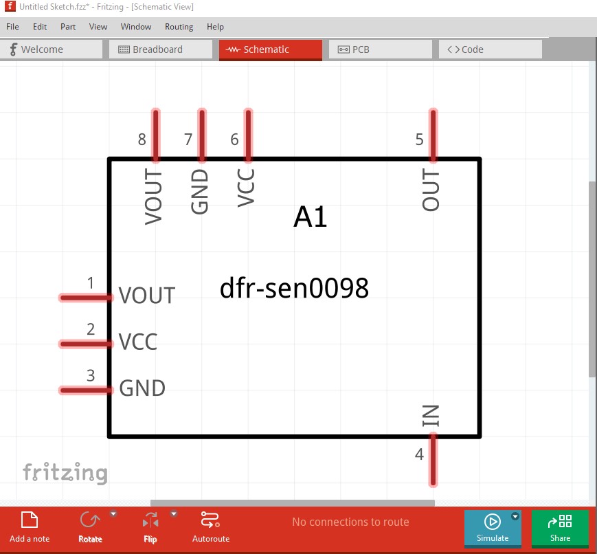
terminalId missing in schematicView (likely an error)
This is indeed and error as we will see when we look at the part.
As is this (except it got flagged as an error)
…
Error 18: File
‘part.PCM1808_39018436c7a78322bff523fa2b4808bb_1.fzp.bak’
Connector connector2terminal is in the fzp file but not the svg file. (typo?)
svg svg.schematic.PCM1808_f5262701827fb87fd599debbd98f8df9_2_schematic.svg.bak
…
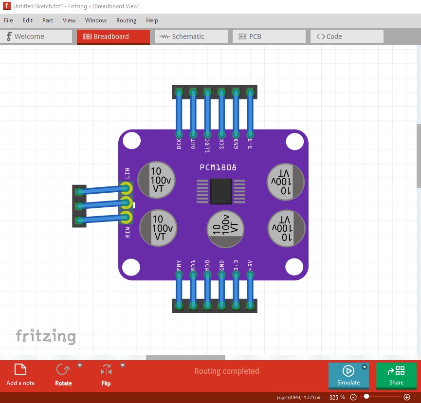
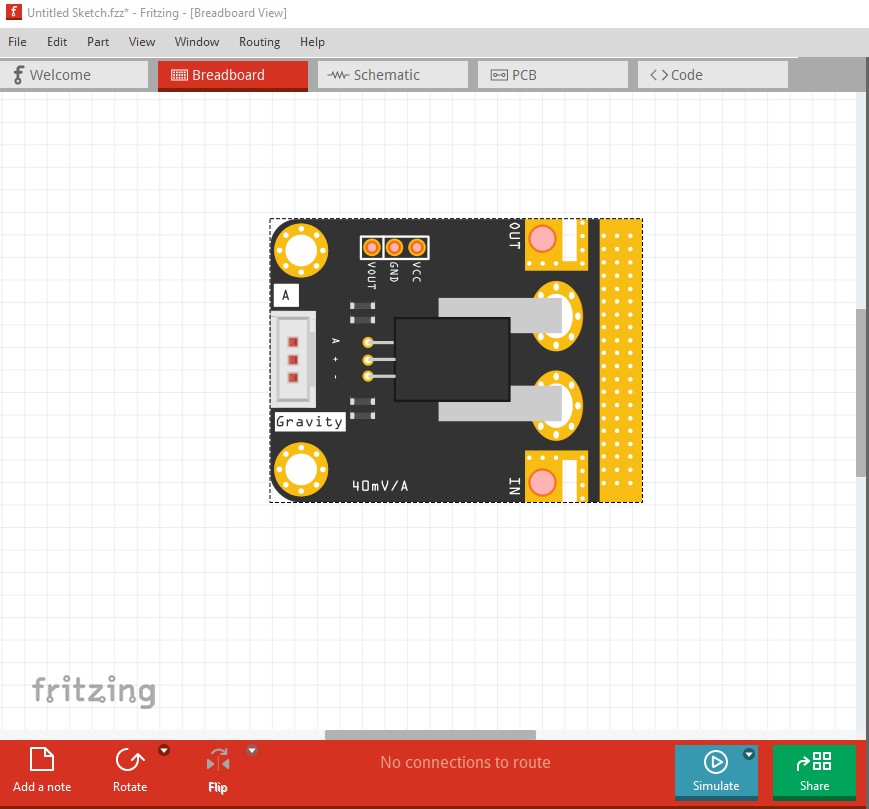
With that lets look at the part and see what the errors cause. Breadboard looks fine.
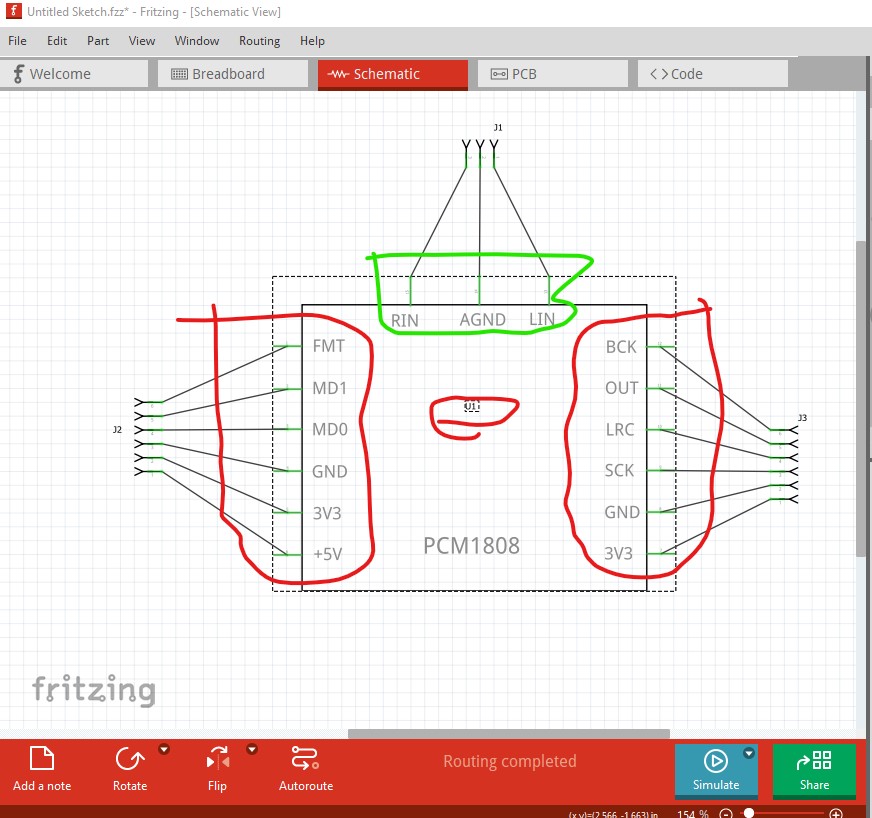
schematic less so. Here we see the problem with no terminalIds, instead of connection to the end of the pin (as the first three pins do) they connect to the center of the pin. Fritzing is supposed to correct this but doesn’t (as in this case) always do so. As well the label on the part is wrong. It is U which indicates an IC, it should be A (for assembly) instead. As well the part is too large, it is preferable to use Randy’ Inkscape extension (detailed in the tutorial) to make schematics as they then meet the graphics standard documents.
edit: replace the wrong image with the correct one …
On to pcb (which is utterly broken)
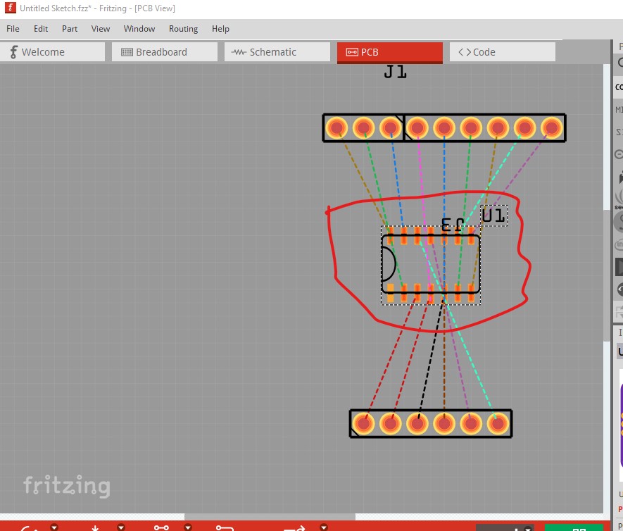
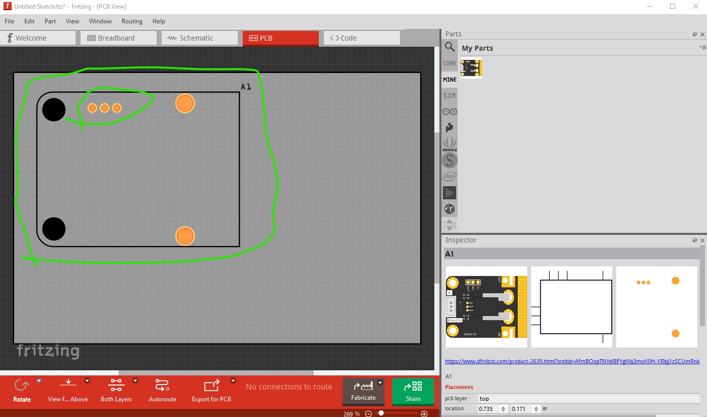
it is a SMD IC rather than the correct output which should be the outline of the board with through hole pads like this
The associated schematic (likely created with Randy’s extension)
and the associated breadboard
Hope this helps, if you have questions feel free to ask.
Peter