Assuming the manual is that on the Fritzing web site, yes it leaves much to be desired. Try these two sets of tutorials (which apply to current Fritizng versions, many of the others are for older versions.) I’d be interested in what is unclear (likely lots!) in mine, as no one has ever commented on it. I generally don’t use parts editor, but Old_Grey’s tutorials cover it.
Usually the pins should be on 0.1in boundaries in breadboard and schematic. Fritzing will pick a pin and align it to the grid, pins that don’t align to that on a 0.1in boundary will be off the grid (there are a few other things that will cause similar problems as well.)
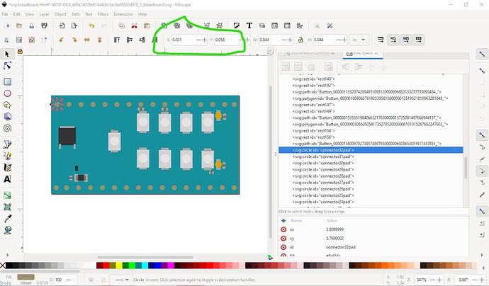
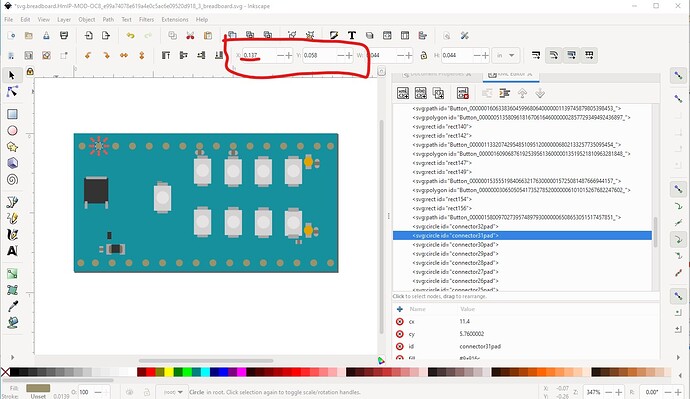
While I don’t use Illustrator, but rather Inkscape, as far as I can see from the online manuals for Illustrator there is no way for the user to control what it does. For Fritzing that can cause scaling problems. Inkscape allows much more control of the output svgs. Although your breadboard svg appears to be correctly dimensioned in inches (as opposed to px which can cause scaling problems. The connectors in the breadboard svg are not on 0.1in boundaries however (this is Inkscape not Illustrator:
connector31 should have an x value of 0.135in not the 0.137in it does have.
That said your part has a number of problems:
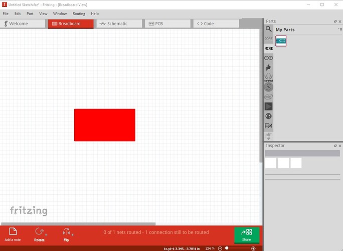
breadboard is pretty much entirely broken (I’m not entirely sure why):
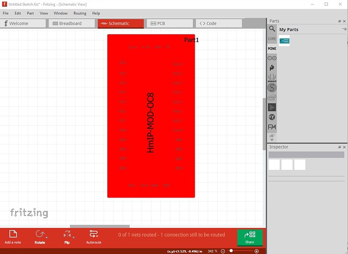
the red rectangle indicates the connectors are not properly defined schematic is much the same:
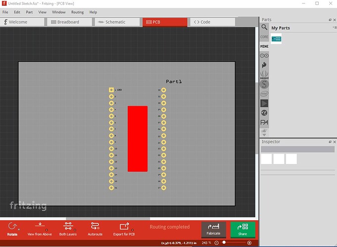
as is pcb
So lets unzip the fzpz and look at the files:
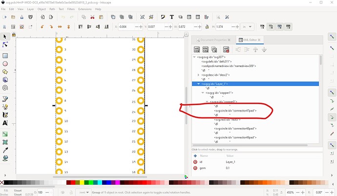
breadboard looks somewhat OK (better than the rendered version for sure. It is likely that the pins should be connectorxpin not connectorxpad (pad is typically SMD in pcb) and indeed the .fzp file indicates they should be defined as pins:
<connector type="male" name="GND1" id="connector1">
 <description>GND1</description>
 <views>
  <breadboardView>
   <p layer="breadboard" svgId="connector1pin"/>
  </breadboardView>
  <schematicView>
   <p layer="schematic" svgId="connector1pin"/>
  </schematicView>
  <pcbView>
   <p layer="copper0" svgId="connector1pin"/>
   <p layer="copper1" svgId="connector1pin"/>
  </pcbView>
 </views>
</connector>
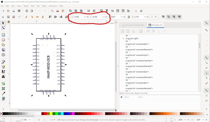
in all three views. The definitions in the .fzp file not matching those in the svgs will cause the problems you are seeing as the connectors are not correctly defined (which causes the red rectangles.) The schematic svg needs to start at 0 0 (I don’t know how to do that in Illustrator, in Inkscape Edit->select all then Edit->Resize drawing to selection will do it.) but it needs to be done. This will also cause offset problems in Fritzing.
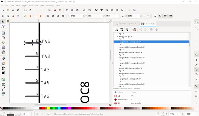
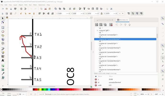
As well your connectors are not correctly defined. The connector0pin looks correct, but connector0terminal is in the wrong place (it should be on the left end of connector0pin.)
I’m not sure why schematic is unhappy (probably pin definitions missing though) Pcb has the pins defined as pad when they need to be pin to match the .fzp file:
I also have a reference to this forum post for Illustrator settings, I don’t know if it will help though:
Hope this helps, if not post again!
Peter
