These two sets of tutorials apply to current versions of Fritzing:
schematic Inkscape plugin
the schematic Inkscape plugin is also extremely useful (I use it for all schematics these days.) That said on to your svg (you can download the svg by right clicking on it and selecting “save file as”.)
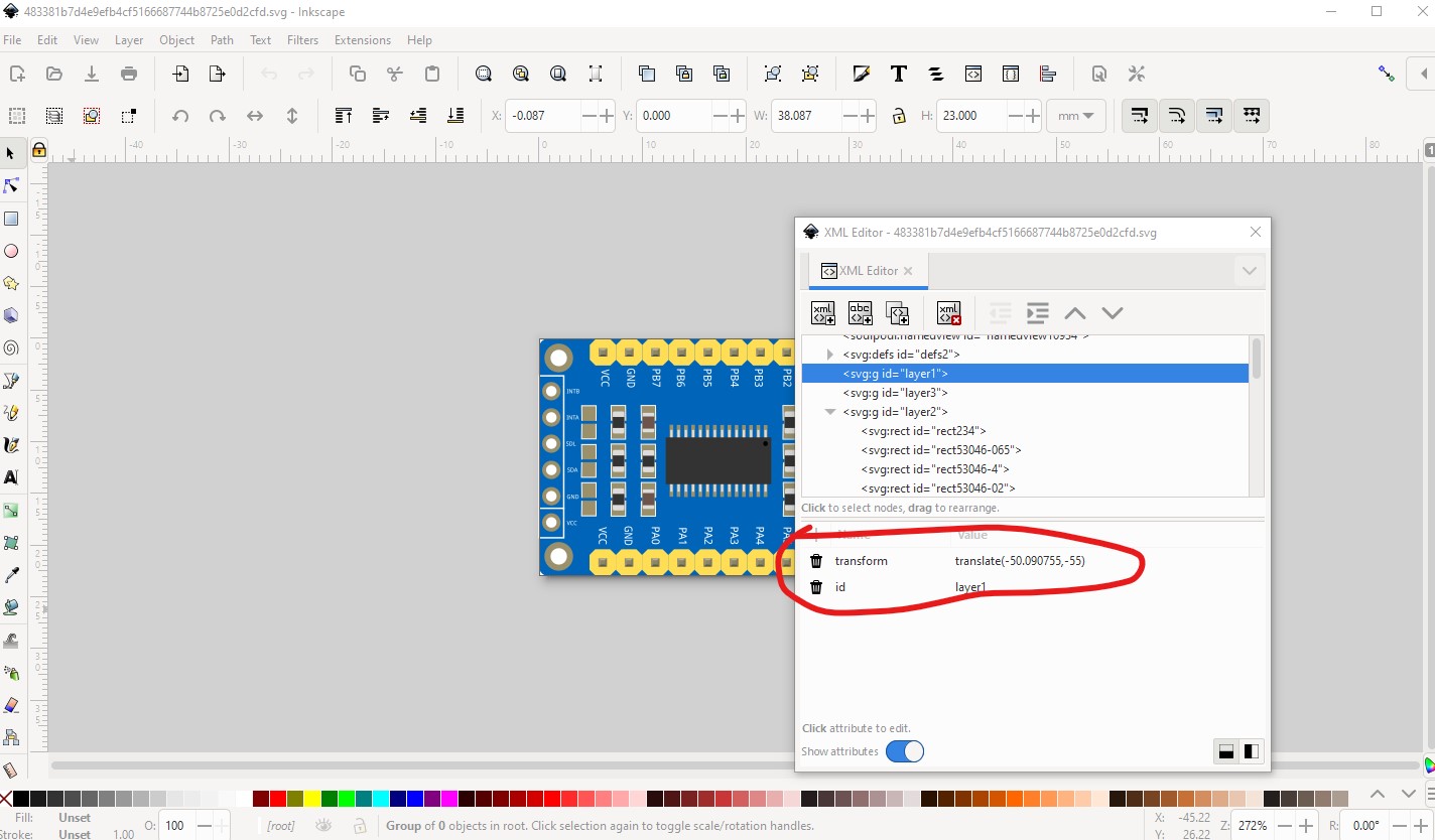
First some basics, a part (.fzpz file) consists of a .fzp file and 3 or 4 svg files. If you unzip a .fzpz you will get these 4 or 5 files (I often reuse breadboard as the icon svg which is why one less svg.) The breadboard svg has only the layerId (a group not a layer in Inkscape terms, I don’t know what layers do in Inkscape since I only use it for Fritzing nor as you will see how to get rid of them!) Next Fritzing uses the tiny svg spec and is often confused by Inkscapeisms, so the recommendation is to save your svg as plain svg rather than Inkscape SVG via the save as option in File. In your svg there is a transform in layer1 that I don’t know how to delete (along with the layer, which I don’t know if Fritzing will react to.)
defs are also a bad idea in Fritzing as it usually deletes them when copying svgs. I think it very likely this isn’t going to work as Fritzing doesn’t support it.
 <defs
     id="defs2">
    <rect
       x="164.39665"
       y="191.36696"
       width="32.508762"
       height="29.496901"
       id="rect80965" />
  </defs>
…
<text
   xml:space="preserve"
   transform="matrix(0.26458333,0,0,0.26458333,-50.090755,-55.000001)"
   id="text80963"
   style="white-space:pre;shape-inside:url(#rect80965);display:inline;fill:#000000;fill-opacity:1;stroke:none;stroke-width:0;stroke-dasharray:none;stroke-opacity:1" />
<polygon
You need to use standard text (nested tspans will also not work correctly) with the Fritzing supported fonts (OCRA and DroidSans, the font files for which are available on the Fritzing site.) Since I can’t figure out how to delete a layer in Inkscape, I resorted to a text editor and just removed the definitions to get a clean svg like this (the def is still there as it is used!)

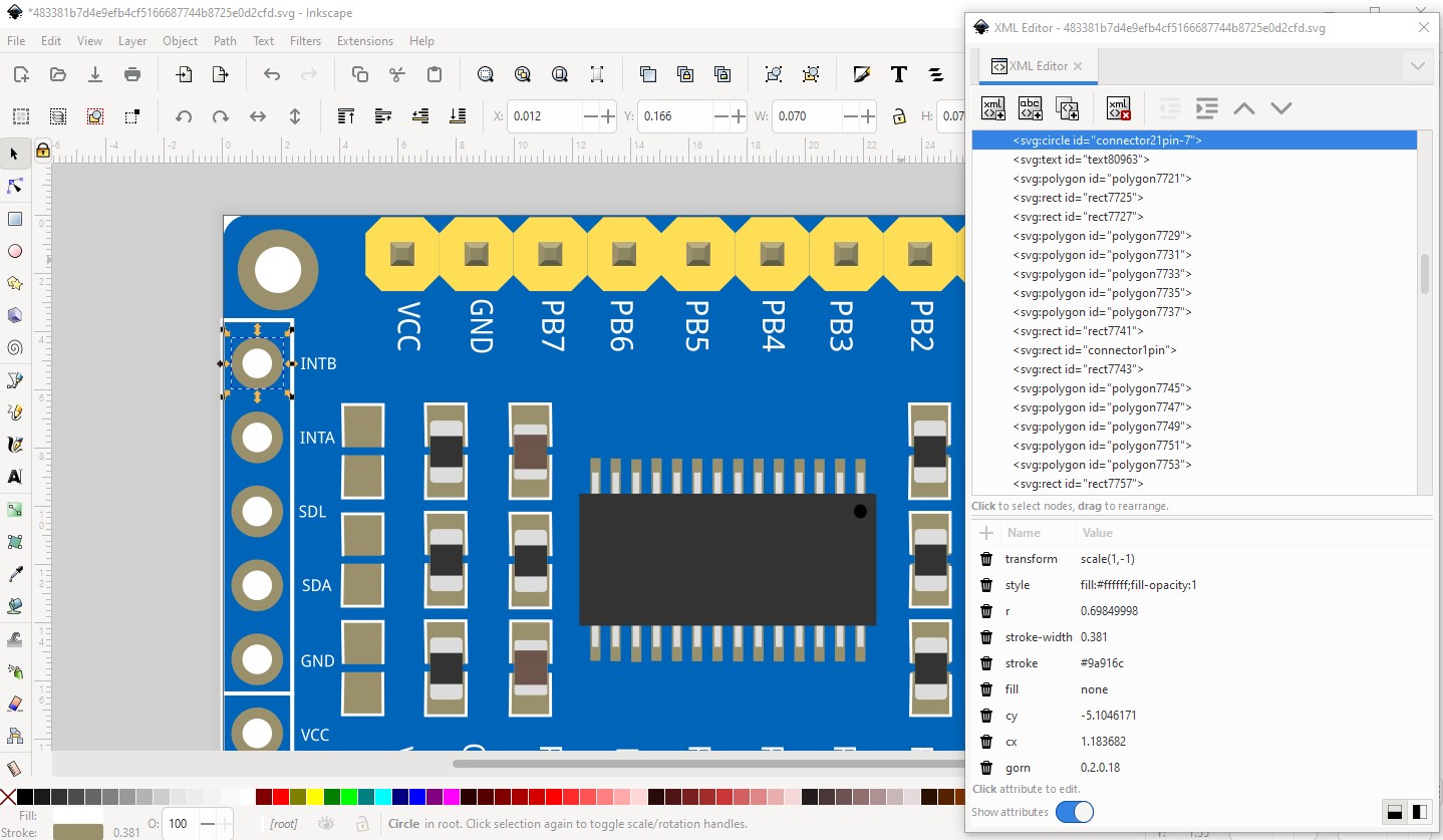
Now on to pins and terminals. In this case the terminals are not needed. The purpose of a terminalId is to mark where a wire should terminate (most commonly in schematic) like this:
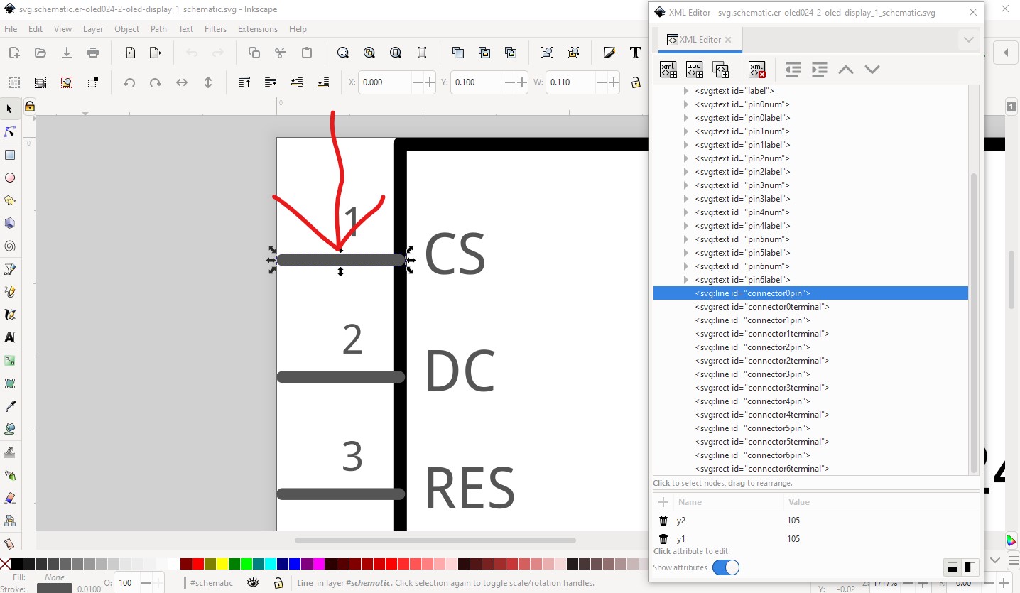
without the terminalId the wire will terminate in the center of the pin (which is wrong!) With the terminalId it will terminate in the center of the terminalId (which is why terminalIds are usually squares) like this:
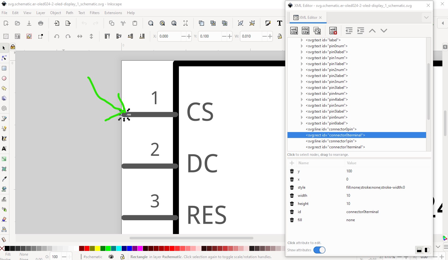
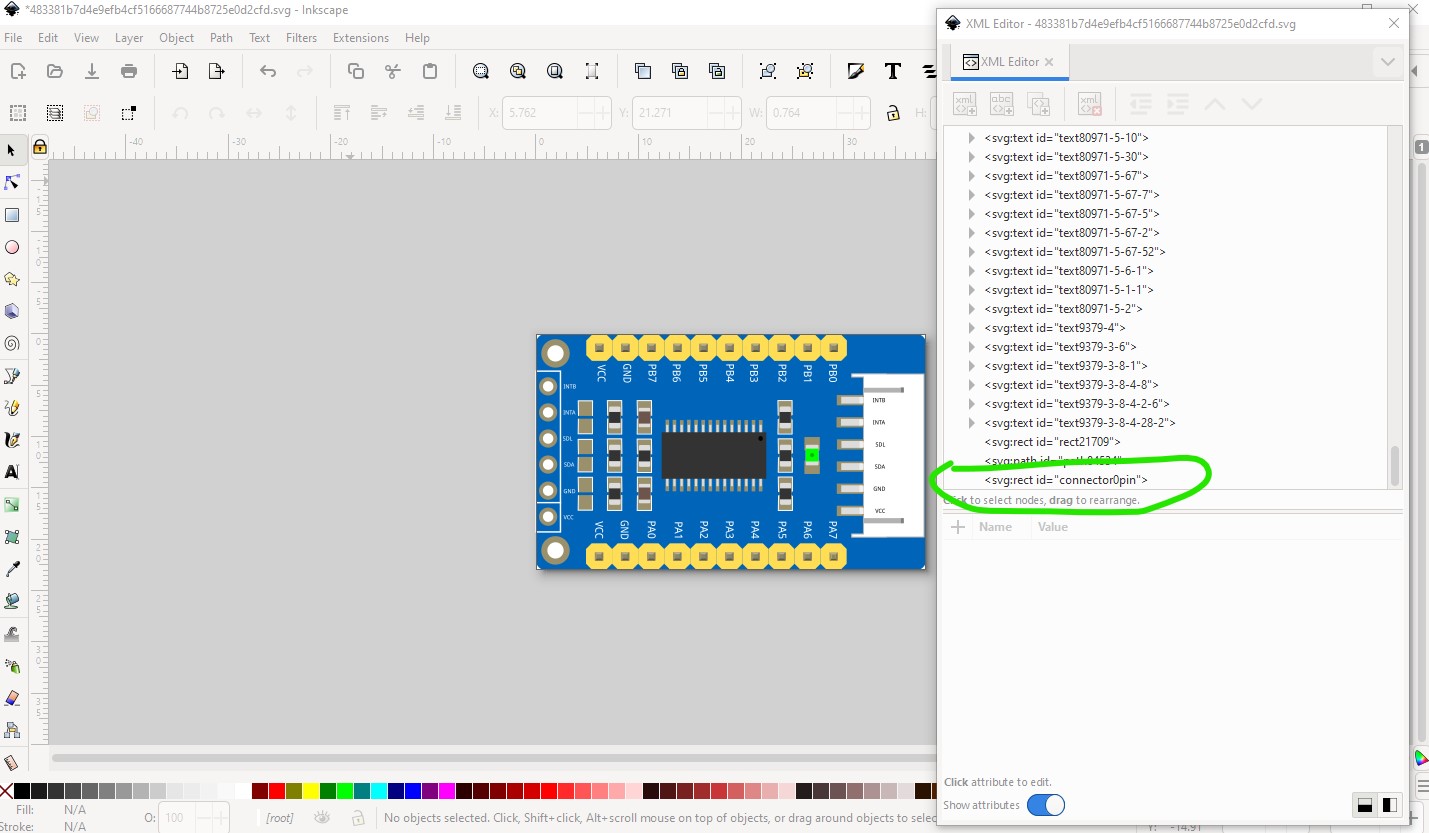
here the wire will terminate on the end of the pin as desired. For a connector in breadboard that is a square or a circle (as opposed to a line as in schematic) you don’t need a terminalId. In this case the parts factory generates (incorrectly in my view!) terminalIds for pins that don’t need them. As long as the appropriate terminalId is defined in the fzp file that however doesn’t matter, it is just sloppy. Pins are supposed to start at connector0 and increase in sequence. However mostly they work with any value (although there are some problems with displaying pin descriptions if the pins are out of order.) so it is preferable that the pins start at connector0 and increase in order. Typically connector0 should be at pin1 on an Ic like this in this case:
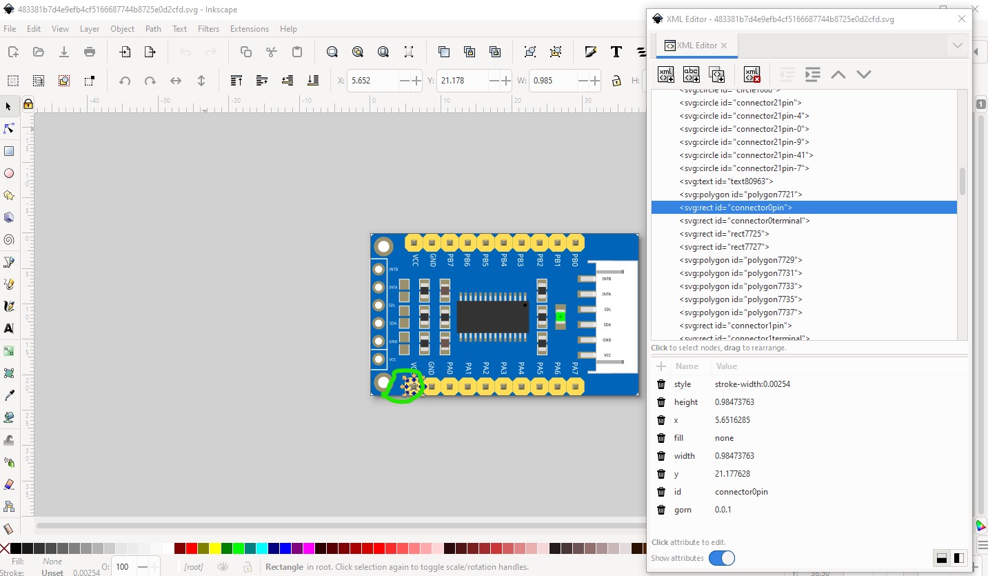
which just happens to be connector0pin as it should be. I would delete the connector0terminal (but you also need to remove it from the fzp file, although it isn’t in the svg it will be just ignored!) I prefer to move the pins to the bottom of the svg like this:
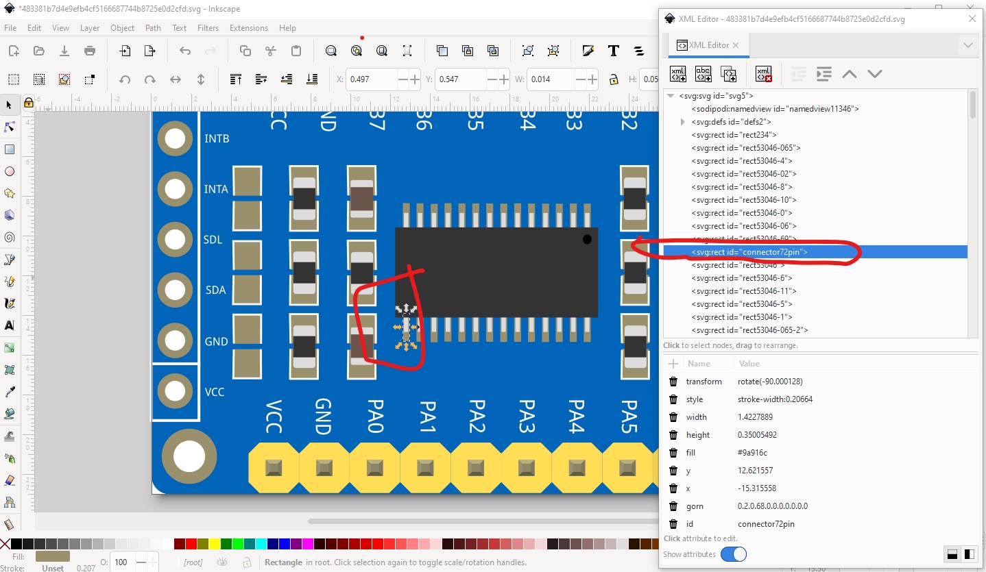
as I have tools that will renumber and move pins in this position (which are not yet publicly available.) This pin doesn’t appear to have a connector definition (and it appears to need one as it is a place that can accept connections.) To correct that I duped connector9pin and moved it via the tool bar (set to inches) like this to keep the new pin on the 0.1in grid. First in x
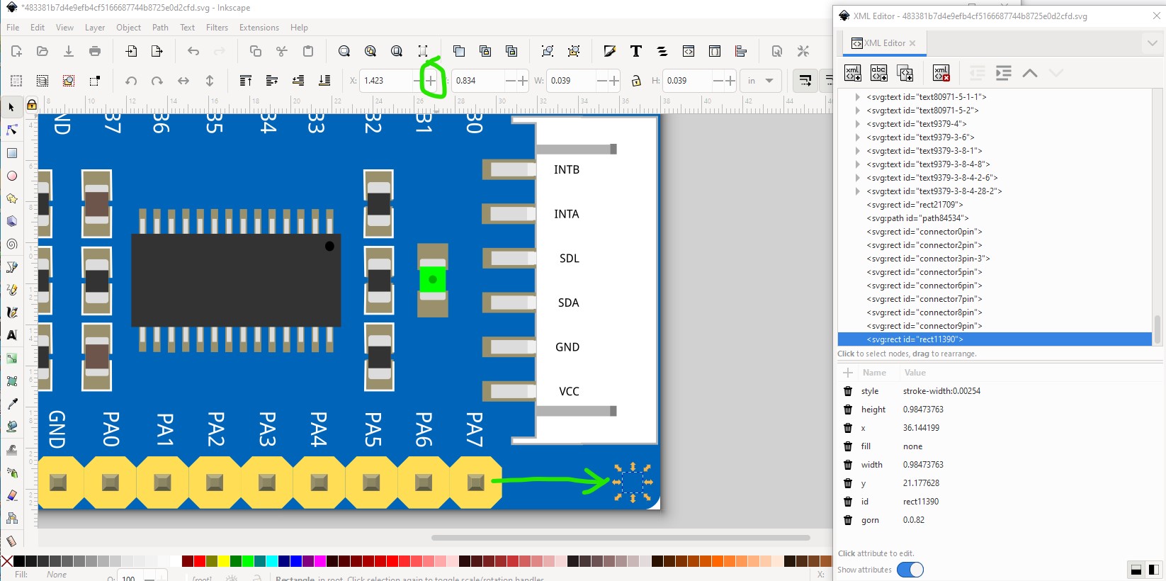
then in y
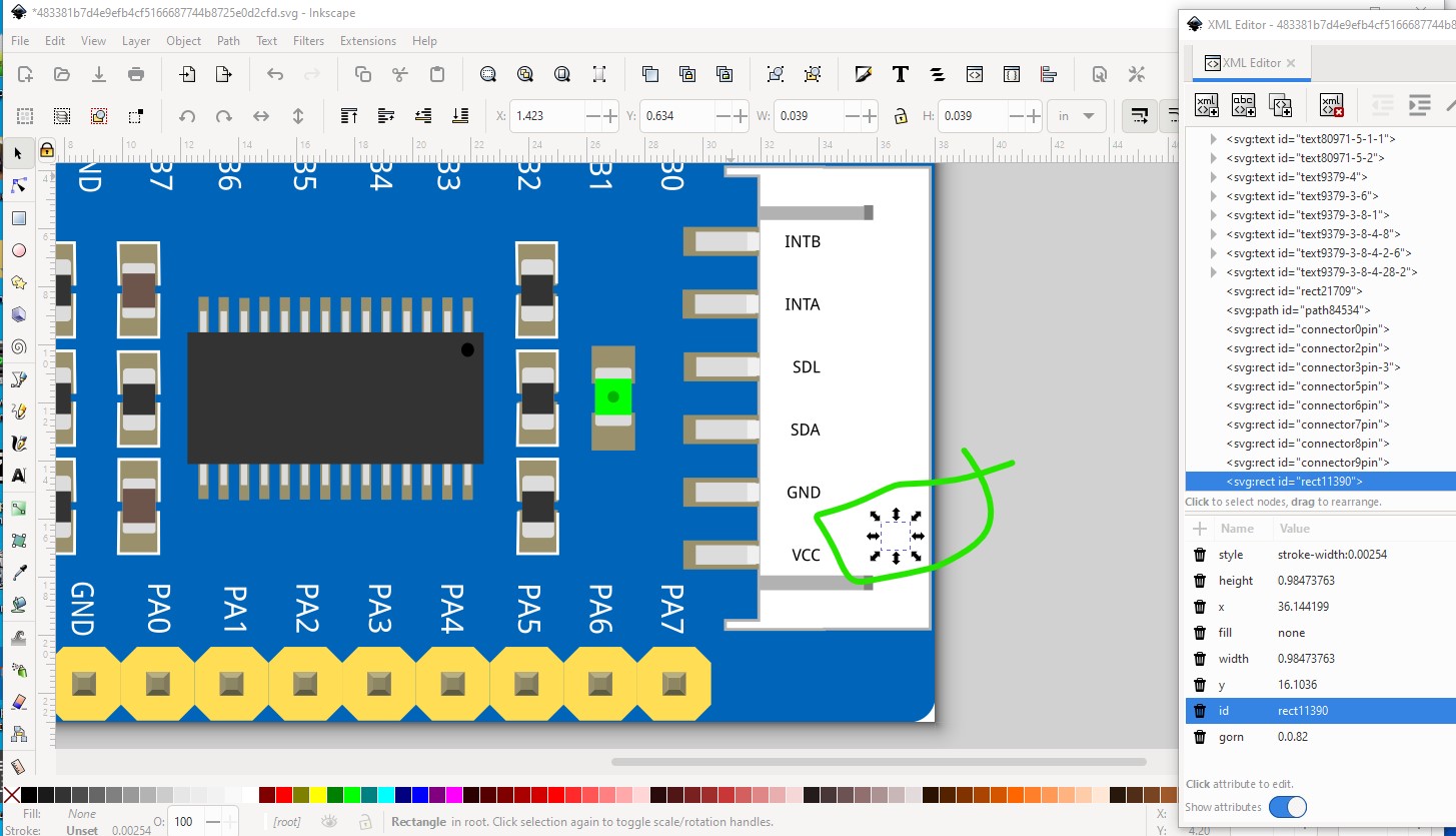
it is a little misaligned with the actual connector, but is on the 0.1in grid which is preferred. Now you need to manually set the id to connector10pin (I would just run a script to renumber the pins when I am finished.) Then duplicate that pin and move it up one position in y to make the next pin, rinse and repeat til done. This looks to be a 2mm connector so the pins are a little misaligned. You could and perhaps should move them to 2mm boundaries. Now on to the top connector:
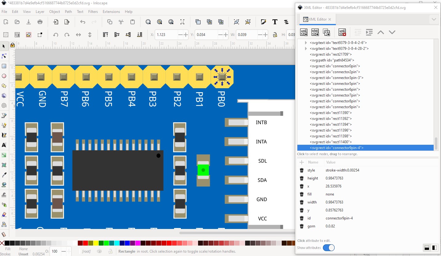
then the end pins
with all the wanted connectors done, we now need to deal with the unwanted connectors. It looks like this svg came from Eagle2Fritzing and thus has extra connectors. Again I have a script (again not yet public) that will remove uneeded connectors and replace them with their element id (circle, rect, etc.) because I use Eagle2Fritzing a lot.
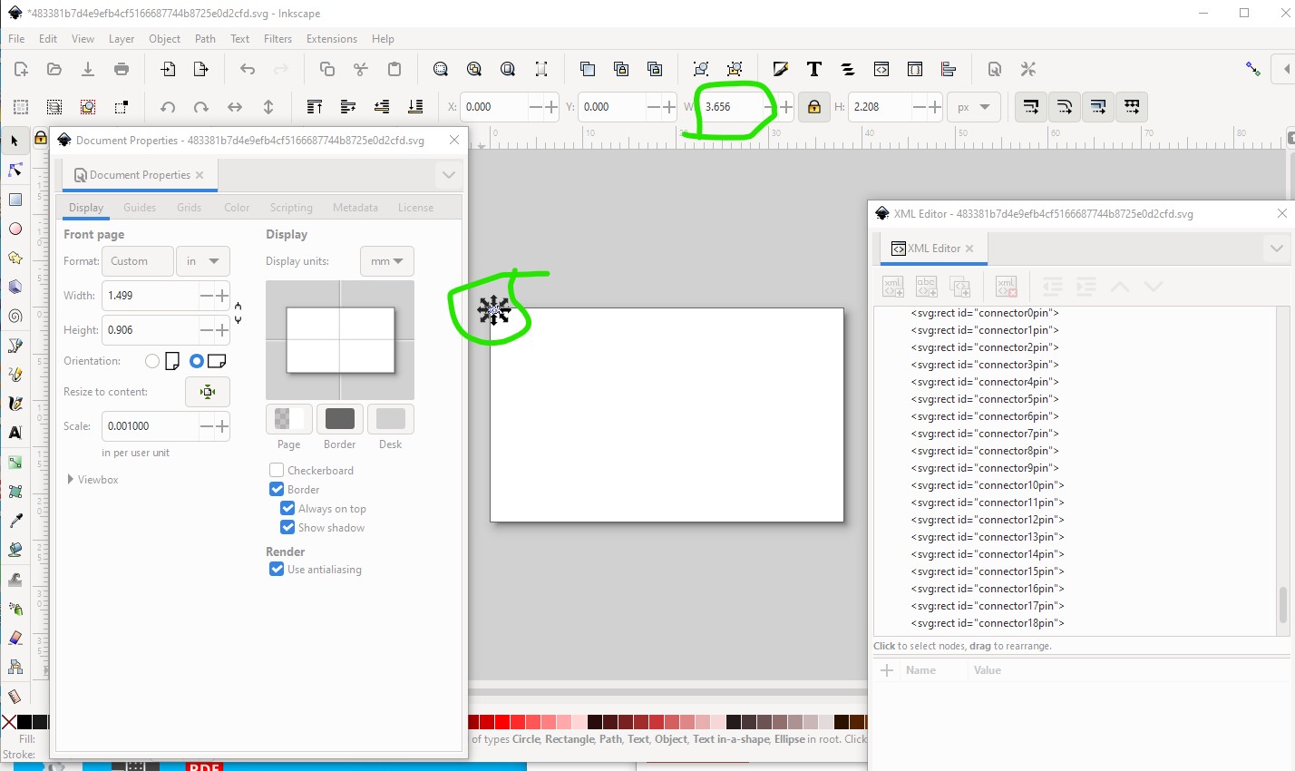
Finally I did Edit->select all, then Edit->resize page to selection to rebuild the svg to start at 0 0 then rescaled the svg by saving the width (in px for maximum resolution) with width locked to height and scale stroke width enabled (the lock of w to h keeps circles circles instead of ellipses!) then modified the scale to be 0.001 (drawing unit = 1 thousandth of an in) as specified in the part file format document.
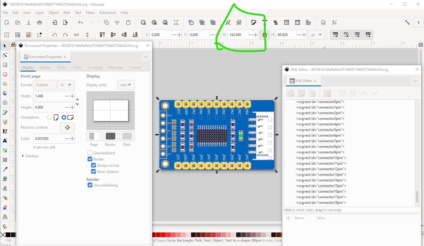
then edit->select all and group to create the breadboard layerId group which in turn when saved as plainsvg creates a valid breadboard svg (other than the def I didn’t remove and maybe the text although the one I looked at is Droid Sans.) Here is the resulting svg:

Note this still needs to be run through FritzingCheckPart.py or to have the px removed from the font-sizes with a text editor before it is suitable for use in Fritzing as with px in the font size Fritizng and/or parts editor will get the font size either too large or too small (set to 0 typically.) Hope this helps.
Peter