Running into two issues using Fritzing, one with custom PCBs, and one with package type

I’m at work, so I can’t provide screenshots right now, but hopefully this is something that doesn’t require it.

Steps I took that resulted in the problem:

  1. Created a custom PCB, and then placed SMD parts on it. The parts appeared reversed, as if they were placed on the bottom side of the PCB, (with the circle indicating pin 1 at the upper right instead of the upper left) even though they were on the top side of the board according to the inspector. I don’t know if this happens with through-hole.

  2. Unable to create TSSOP-16 parts. The default 74HC595 part does not allow me to select TSSOP-16 as the package type. So I chose a generic IC, set it to 16 pins, and then set it to TSSOP. When I do that, it sets it to TSSOP, but with 20 pins. So I chose 16 pins from the dropdown, and the part reverted to SO(w)-16. I am unable to create a TSSOP-16 part.

My version of Fritzing and my operating system:

0.94

Welcome aboard! There appears to be an oddness about the 75hc595 part. The THT version does not allow switching to the SMD version via inspector (and will let you switch to a 14pin dip, but then changes the chip type which is a bug.) To get the SMD version you need to do a search in core parts and select the SMD version like this:

As you see the chip is on the top of the board as it should be. If you upload the sketch (the .fzz file) via the 7th icon from the left in the reply menu I’ll have a look at what is going on in your sketch.

Peter

Thanks Peter. When I’m back home I’ll upload it.

Board - Custom PCB.fzz (9.3 KB)

Hi Peter, here is the file.

EDIT: Just checked the SMD version of the 74HC595, and it only allows for the SO package and DIP package.

EDIT 2: I think it’s just because I had “view from below” on.

That will do it. The sketch looks fine to me. What package do you need for the 74hc595? It is relatively easy for me to make a new part with a different footprint. I’m going to guess you are looking for the tssop14 (looking at the TI datasheet.) and I think there should be one around.

Peter

It’s 16 pins, so the TSSOP-16 is the package.

Thanks!
Greg

OK this should do the trick. Best to print out the pcb foot print at 1:1 scale and check it against a real part, but it looks to match the TI data sheet for a tssop16 case. I was lazy and kept the dip outline in breadboard, rather than one of the smd carriers which is the correct answer.

The part

74HC595-SMD-tssop16.fzpz (6.1 KB)

and a test sketch for it (I checked the gerber output is ok as well.) To my surprise the default DRC rules pass with 8mil traces and a grid size of 0.01in

test-Sketch.fzz (14.9 KB)

Peter

Thanks, Peter. This is fantastic work. Quick question though, I compared the TSSOP-20 part tot he one you just created. They are very close, but the TSSOP part has a tiny incremental error in alignment of the pads that causes a pretty significant shift in the pad location towards the bottom.

It looks correct according to the TI data sheet. Pitch is 0.65mm, and 5.8mm center to center. The footprint is from a Sparkfun part and they are usually accurate.

edit: do you perhaps have a 0.5mm tssop? That would do this. In which case I’d need to know whose 74hc595 you are using, its possibly different than TI (which is the first data sheet I found.)

Peter

Hi Peter,

I am using TI’s SN74HC595, and I verified that the specs in the sheet are the specs you’ve mentioned.

I checked Wikipedia and TI’s website, and it said that their TSSOP pitches range from roughly 0.45mm to 0.65mm, so I guess the package determines the pitch, and likely the TSSOP-20 has a different pitch than the 16 pin package, so I think it’s safe to say your footprint is correct.

Thanks again.
Greg

Hi Peter, can you create a VQFN-28 package for the generic IC? Here are the details (page 26) https://www.mouser.com/datasheet/2/268/Atmel-8271-8-bit-AVR-Microcontroller-ATmega48A-48P-1315288.pdf

If not, I understand. Can you point me to a good tutorial on how to create custom pads/parts?

Sure, not that hard. First find a qfn 28 footprint to start from in this case I used

fritzing-parts\svg\core\pcb\sparkfun-digitalic__stn_scantool_qfn-28-s_pcb.svg

from core parts. It is too big, 0.065mm pitch (needs 0.045 pitch) so edit in Inkscape. Get the recommended footprint from

page 12

pin 28 body 4x4 pitch 0.45 (which matches the data sheet)

adjust the pads and thermal pad to match this layout in Inkscape (used the data sheet thermal pad size not the footprint pdf one as it is specific to IC)

change connector0 from

w 8.5mm h 0.35mm

to

w 0.8mm h 0.25mm

repeat on connector 27 (the alternate orientation)

save the svg and edit the svg with vi. copy the height and width of connector0 and connector27 to all their same pins so all the pins are the correct size (but not the correct pitch or position yet.) Edit the modified svg with Inkscape. Set construction lines like this:

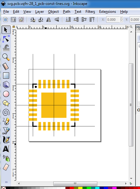
(the real svg appears to be too small for the forum to upload, so I’ll use an fzpz file later.) Now move the center pin to be centered in x and y with the center lines, then adjust the pins above and below (by changing their x and y values in the tool bar) to be on 0.45mm pitch. Then remove the construction lines, edit select all, resize page to drawing. Now regroup the silk screen and copper1 layers and save as plain svg.

VQFN-28-footprint.fzpz (3.1 KB)

if you download and unzip the .fzpz file you will get two svgs:

svg.pcb.vqfn-28_1_pcb.svg

which is the footprint you want and

svg.pcb.vqfn-28_1_pcb-const-lines.svg

which is the image above with the construction lines present to see how I did it. The original svg I used will be in your Fritzing core parts directory. To use the footprint it is probably easiest to use parts editor on the generic IC (it needs to be a 28pin smd of some kind) and replace the pcb svg with svg.pcb.vqfn-28_1_pcb.svg above. You can (which is what I would usually do :slight_smile: ) also create the generic IC in the mine parts bin, then right click it and export part to write the fzpz file. Unzip that file and copy svg.pcb.vqfn-28_1_pcb.svg in to the pcb.svg.xxxxx.pcb file in the unizipped directory and rezip it as a .fzpz file and reload it in to Fritzing. As to parts making tutorials these two apply to the latest Fritzing version:

Peter

Ok, so despite my best efforts, I was not able to create an 0201 SMD resistor. I used the 0402 svg as a template, and used this as a reference for how big the parts need to be:

I scaled the parts down to match the dimensions shown, but when I actually tried to import the svg into the parts editor, the pads did not show up in yellow like they usually do. Any idea what I may have done wrong?

If you can post the svg file for the part I’ll have a look (upload is 7th icon from the left on the reply menu.) If it tells you it can’t determine the size of the svg (which it probably will), zip the svg and change the .zip to .fzpz and up load that. If it does upload the svg in the reply menu you will see a pixel value which is usually tiny (such as 12) multiply the sizes by 10 or 100 (i.e 100200 or 10002000) and the svg will work a lot better. I think with the small parts the size becomes 00 which is why the “can’t determine the size” message.

Peter

sparkfun-passives_0201-res_pcb.fzpz (1.2 KB)

Let me know if that works. Thanks.

Sorry for the later reply, my network connection has been down most of the day. The svg made it here fine. There are a couple of problems, mostly that the copper1 group has no members. In Inkscape it looks like this:

Silkscreen should be above copper1, not below it (although that won’t cause much harm) but copper1 has no members so the connectors are not in copper1 and thus Fritzing won’t see them. I tried correcting this, but the transforms interfere. Here I used the indent node icon in xml editor (circled in red) to add the connectors to copper1, but as we see from the image, the transforms move things:

So instead I ungrouped copper1 which was empty and moved silkscreen above the two connectors

Note silkscreen has a transform (circled in red in xml editor) sometimes the gerber code ignores them, so I prefer to remove them. Ungrouping Silkscreen will do that.

with no groups, none of the elements have translates, so now I will regroup them, here none of the groups have a translate and this svg should load correctly (I also changed the silkscreen color to black which is now correct, although the present color won’t cause any problem.)

The svg it too small for the forum to load, so I zipped it in to a .fzpz too.

sparkfun-passives_0201-res_pcb-fixed.fzpz (797 Bytes)

Peter

sparkfun-digitalic_mlf28_pcb.fzpz (1.8 KB)
Okay, here is attempt 2 at a custom part, and MLF-28 package for the ATMega328. I’ve been careful about it, but when I import it into the parts editor, it says it does not support multiple copper layers. I’m not sure what the issue is. Also, can you elaborate again on how to give something a new footprint? I placed an SMD version of the 328 on the board, tried parts editor, loaded a new graphic into the PCB view, saved it, but couldn’t find it anywhere.

Thanks
Greg

Easy one :slight_smile: you have a stray copper0 group:

Delete that and the problem should clear. As well silkscreen should be above copper1. It will work fine like this, but select in pcb prefers the bottom group first and you almost never want to select silkscreen, so the copper groups on the bottom is best.

Peter