Pretty good, but a few problems. In breadboard You need to create a group of the entire svg and name it breadboard like this:
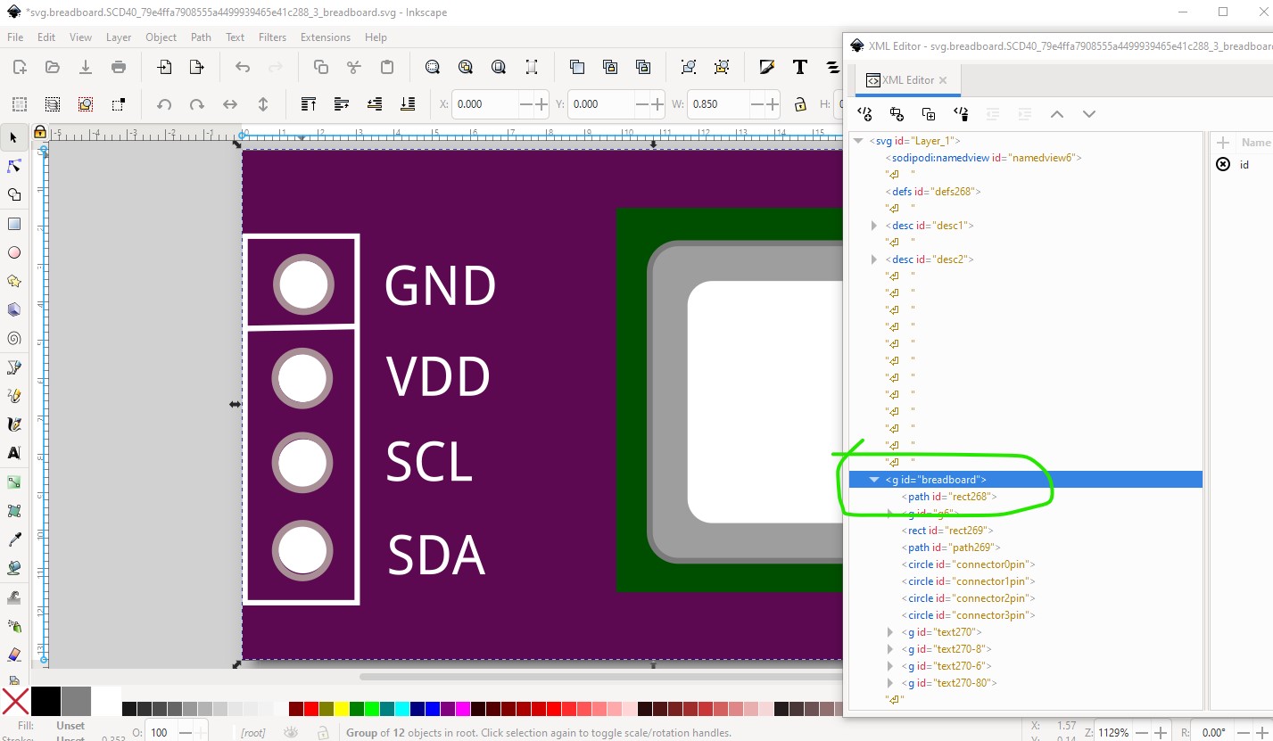
if the layerId is missing the part won’t export as an image (breadboard for this part will be blank!)
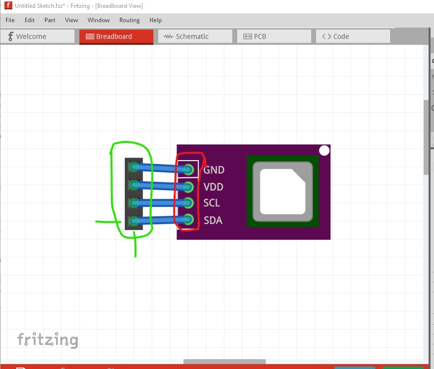
the connectors need to be on 0.1in boundaries and they are not. That causes an offset from the connecting wire:
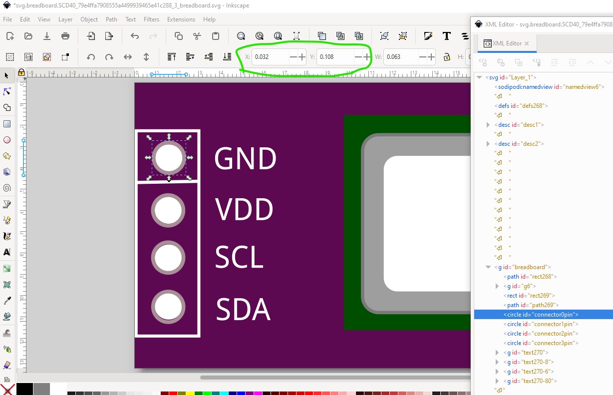
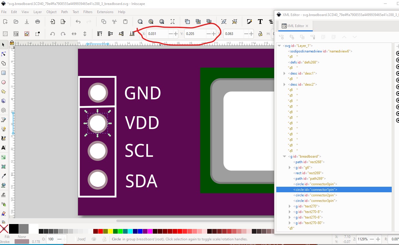
If I start on connectoropin connector1pin should be 0.032 in X and 0.208 (not the current 0.031in and 0.205in)
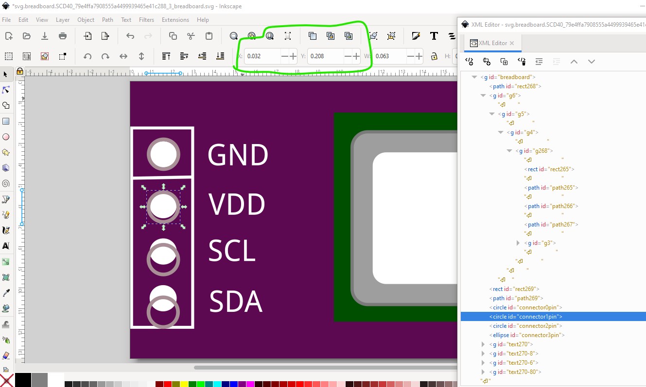
here all the pins have been properly positioned. It is better to set a fill of #ffffff (white) in the circle and not put an underlying circle in the path as that makes the pins easier to change as we see here. If the fill was set to #ffffff I could have corrected this by just positioning the connectors correctly.
Here is the effect in breadboard view. Note that the wires from the header connector are mostly misaligned (only SCL is correct because Fritzing has chosen to align that pin to the 0.1in grid.
schematic is good except for the lack of terminalIds which causes this:
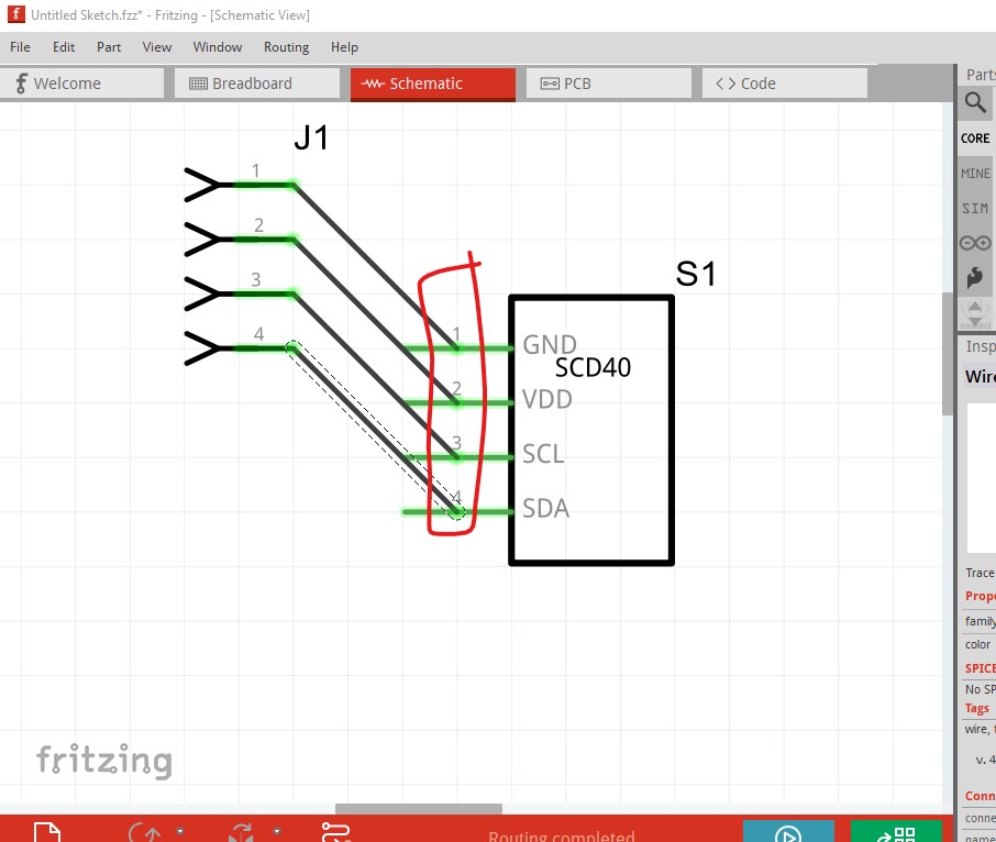
instead of connecting to the end of the pin (typically a square the size of the pin and aligned on the end of the pin and labeled connectorxteminal) the wire connects to the center of the pin which in this case is incorrect. While your pcb will work fine, it is preferred to copy breadboard to pcb and then change the path that is the board to have a fill of none, a stroke of #000000 and a stroke-width 0f 10thousands of an inch to provide a pcb that looks like this:
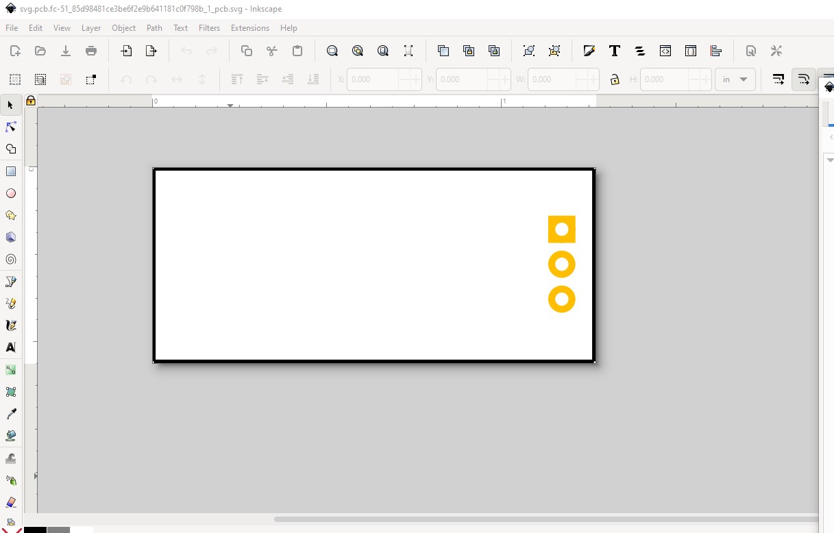
so you can mount the board on a pcb and its outline will show up in silkscreen to tell you where it will be. This tutorial (if you haven’t seen it) covers all these issues
https://forum.fritzing.org/t/part-creation-howto-part-1-breadboard-and-pcb/7692
it also points to a part checking tool which will flag most of the errors I noted (it won’t catch the pins being not on 0.1in boundaries at present.) As we see the output is fairly large and not all that readable (because it is referencing source lines in the input svg files which is all it has!) but it does indicate all the errors except the mis alignment in breadboard as noted:
$ FritzingCheckPartw.py part.SCD40_79e4ffa7908555a4499939465e41c288_3.fzp
**** Starting to process file Startup, no file yet
**** Starting to process file part.SCD40_79e4ffa7908555a4499939465e41c288_3.fzp
**** Starting to process file svg.breadboard.SCD40_79e4ffa7908555a4499939465e41c288_3_breadboard.svg.bak
**** Starting to process file svg.schematic.SCD40_79e4ffa7908555a4499939465e41c288_3_schematic.svg.bak
**** Starting to process file svg.pcb.SCD40_79e4ffa7908555a4499939465e41c288_3_pcb.svg.bak
File
‘part.SCD40_79e4ffa7908555a4499939465e41c288_3.fzp.bak’
This is a through hole part as both copper0 and copper1 views are present.
If you wanted a smd part remove the copper0 definition from line 48
Modified 4: File
‘svg.breadboard.SCD40_79e4ffa7908555a4499939465e41c288_3_breadboard.svg.bak’
At line 6
ReferenceFile
‘SCD41 CO2 rev B_breadboard.svg’
doesn’t match input file
‘SCD40_79e4ffa7908555a4499939465e41c288_3_breadboard.svg’
Corrected
Modified 4: File
‘svg.schematic.SCD40_79e4ffa7908555a4499939465e41c288_3_schematic.svg.bak’
At line 5
ReferenceFile
‘generic_sip_4_300mil_schem.svg’
doesn’t match input file
‘SCD40_79e4ffa7908555a4499939465e41c288_3_schematic.svg’
Corrected
Modified 4: File
‘svg.pcb.SCD40_79e4ffa7908555a4499939465e41c288_3_pcb.svg.bak’
At line 5
ReferenceFile
‘jumper_4_100mil_pcb.svg’
doesn’t match input file
‘SCD40_79e4ffa7908555a4499939465e41c288_3_pcb.svg’
Corrected
Modified 3: File
‘svg.pcb.SCD40_79e4ffa7908555a4499939465e41c288_3_pcb.svg.bak’
At line 17
Silkscreen, converted stoke from white to black
Modified 3: File
‘svg.pcb.SCD40_79e4ffa7908555a4499939465e41c288_3_pcb.svg.bak’
At line 18
Silkscreen, converted stoke from white to black
Modified 3: File
‘svg.pcb.SCD40_79e4ffa7908555a4499939465e41c288_3_pcb.svg.bak’
At line 19
Silkscreen, converted stoke from white to black
Modified 3: File
‘svg.pcb.SCD40_79e4ffa7908555a4499939465e41c288_3_pcb.svg.bak’
At line 20
Silkscreen, converted stoke from white to black
Modified 3: File
‘svg.pcb.SCD40_79e4ffa7908555a4499939465e41c288_3_pcb.svg.bak’
At line 21
Silkscreen, converted stoke from white to black
Warning 6: File
‘part.SCD40_79e4ffa7908555a4499939465e41c288_3.fzp.bak’
At line 2
ReferenceFile name
‘generic_sip_4_300mil.fzp’
Doesn’t match fzp filename
‘SCD40_79e4ffa7908555a4499939465e41c288_3.fzp’
Warning 7: File
‘part.SCD40_79e4ffa7908555a4499939465e41c288_3.fzp.bak’
At line 2
No Fritzing version in fzp file
Warning 32: File
‘svg.breadboard.SCD40_79e4ffa7908555a4499939465e41c288_3_breadboard.svg.bak’
At line 3
Scale is not the desirable 1/1000 ratio from width/height to
viewBox width/height.
Warning 23: File
‘svg.breadboard.SCD40_79e4ffa7908555a4499939465e41c288_3_breadboard.svg.bak’
At line 38
Key -inkscape-font-specification
value ‘Lucida Console Semi-Condensed’ is invalid and has been deleted
Warning 25: File
‘svg.pcb.SCD40_79e4ffa7908555a4499939465e41c288_3_pcb.svg.bak’
At line 16
Silkscreen layer should be above the copper layers for easier selection
in pcb view
Error 69: File
‘svg.breadboard.SCD40_79e4ffa7908555a4499939465e41c288_3_breadboard.svg.bak’
At line 9
Found a drawing element before a layerId (or no layerId)
Error 18: File
‘part.SCD40_79e4ffa7908555a4499939465e41c288_3.fzp.bak’
Connector connector0terminal is in the fzp file but not the svg file. (typo?)
svg svg.breadboard.SCD40_79e4ffa7908555a4499939465e41c288_3_breadboard.svg.bak
Error 18: File
‘part.SCD40_79e4ffa7908555a4499939465e41c288_3.fzp.bak’
Connector connector1terminal is in the fzp file but not the svg file. (typo?)
svg svg.breadboard.SCD40_79e4ffa7908555a4499939465e41c288_3_breadboard.svg.bak
Error 18: File
‘part.SCD40_79e4ffa7908555a4499939465e41c288_3.fzp.bak’
Connector connector2terminal is in the fzp file but not the svg file. (typo?)
svg svg.breadboard.SCD40_79e4ffa7908555a4499939465e41c288_3_breadboard.svg.bak
Error 18: File
‘part.SCD40_79e4ffa7908555a4499939465e41c288_3.fzp.bak’
Connector connector3terminal is in the fzp file but not the svg file. (typo?)
svg svg.breadboard.SCD40_79e4ffa7908555a4499939465e41c288_3_breadboard.svg.bak
Modified 2: File
‘svg.schematic.SCD40_79e4ffa7908555a4499939465e41c288_3_schematic.svg.bak’
At line 13
Connector connector0terminal had a zero width, set to 10
Check the alignment of this pin in the svg!
Modified 2: File
‘svg.schematic.SCD40_79e4ffa7908555a4499939465e41c288_3_schematic.svg.bak’
At line 18
Connector connector1terminal had a zero width, set to 10
Check the alignment of this pin in the svg!
Modified 2: File
‘svg.schematic.SCD40_79e4ffa7908555a4499939465e41c288_3_schematic.svg.bak’
At line 23
Connector connector2terminal had a zero width, set to 10
Check the alignment of this pin in the svg!
Modified 2: File
‘svg.schematic.SCD40_79e4ffa7908555a4499939465e41c288_3_schematic.svg.bak’
At line 28
Connector connector3terminal had a zero width, set to 10
Check the alignment of this pin in the svg!
Hope this helps!
Peter