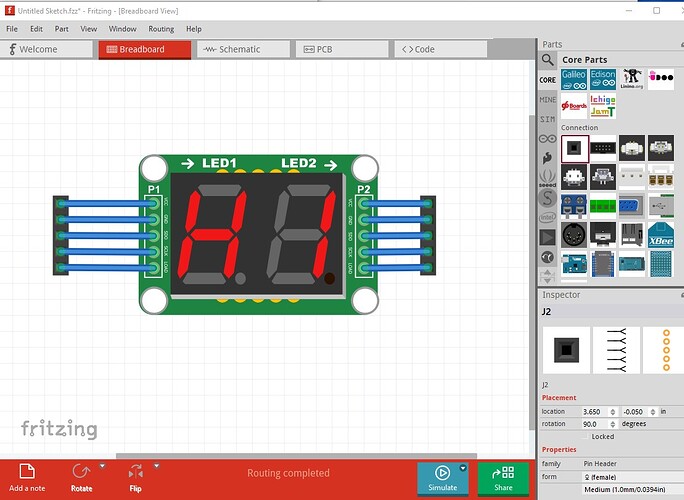
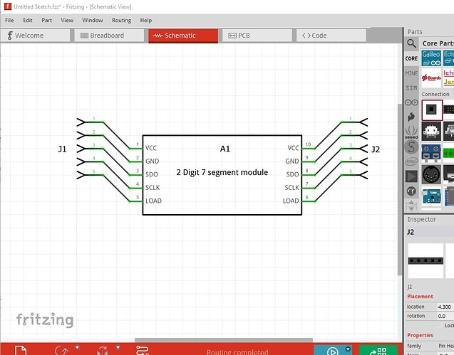
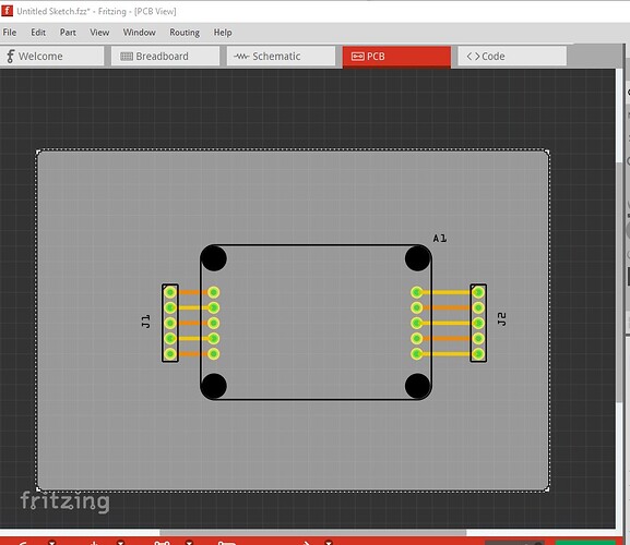
Not a bad job, but there are several issues that can be improved.
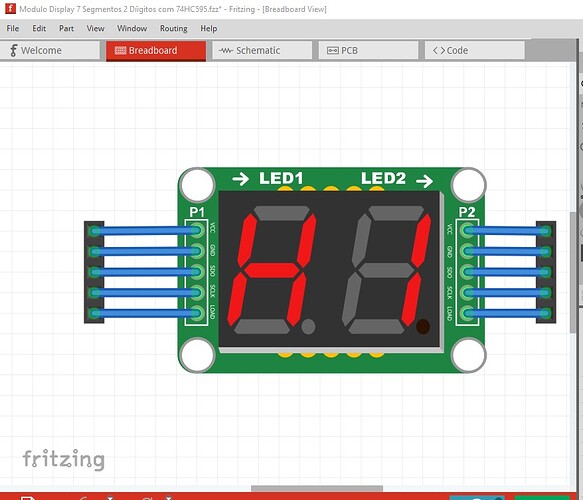
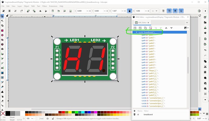
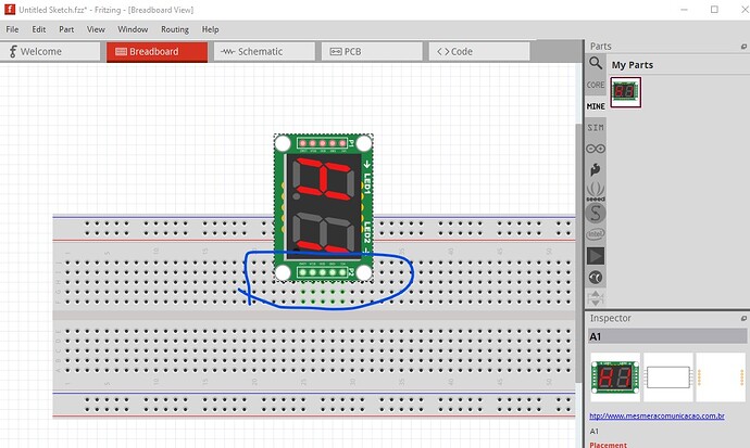
breadboard appears fine
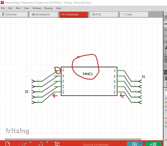
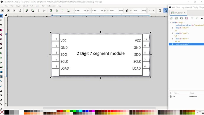
schematic has issues
the label field in the ,fzp file should be A (for assembly) as this is a module. The pins should align with the 0.1in grid (which they may with proper terminalIds I haven’ yet looked at the svg files.) Without a terminalId the wire will terminate in the center of the pin (and that may be what snapped to the grid in this case)
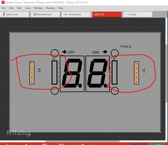
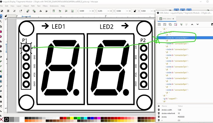
pcb should have pins (and typically no text except a board outline) because if you want text you can (and should!) add it in the sketch. To remove the text in this case you would have to modify the part. As well you should post the .fzpz file for the part rather than the .fzz file (which is the sketch.) The .fzpz file can be recovered from the sketch by exporting it from the temp part bin (which is populated by the .fzz file on load) like this
right click on the part and select “export part” and it will write the part to a .fzpz file. It is easier to just be able to download the .fzpz file rather than needing to download the sketch, load it and export the part. Running your part through FritzingCheckPart.py (which is referred to in this tutorial on making parts)
$ FritzingCheckPartw.py ‘part.Display 7 Segments Module - 2 Digits with 74HC595_20a9453f0f3e3d965b2bff094cca9880_8.fzp’
**** Starting to process file Startup, no file yet
(and ignoring the warning messages which won’t cause a part to not work!)
Error 69: File
‘svg.breadboard.Display 7 Segments Module - 2 Digits with 74HC595_20a9453f0f3e3d965b2bff094cca9880_8_breadboard.svg.bak’
At line 19
Found a drawing element before a layerId (or no layerId)
Error 18: File
‘part.Display 7 Segments Module - 2 Digits with 74HC595_20a9453f0f3e3d965b2bff094cca9880_8.fzp.bak’
Connector connector0terminal is in the fzp file but not the svg file. (typo?)
svg svg.breadboard.Display 7 Segments Module - 2 Digits with 74HC595_20a9453f0f3e3d965b2bff094cca9880_8_breadboard.svg.bak
Error 18: File
‘part.Display 7 Segments Module - 2 Digits with 74HC595_20a9453f0f3e3d965b2bff094cca9880_8.fzp.bak’
Connector connector1terminal is in the fzp file but not the svg file. (typo?)
svg svg.breadboard.Display 7 Segments Module - 2 Digits with 74HC595_20a9453f0f3e3d965b2bff094cca9880_8_breadboard.svg.bak
Error 18: File
‘part.Display 7 Segments Module - 2 Digits with 74HC595_20a9453f0f3e3d965b2bff094cca9880_8.fzp.bak’
Connector connector2terminal is in the fzp file but not the svg file. (typo?)
svg svg.breadboard.Display 7 Segments Module - 2 Digits with 74HC595_20a9453f0f3e3d965b2bff094cca9880_8_breadboard.svg.bak
Error 18: File
‘part.Display 7 Segments Module - 2 Digits with 74HC595_20a9453f0f3e3d965b2bff094cca9880_8.fzp.bak’
Connector connector3terminal is in the fzp file but not the svg file. (typo?)
svg svg.breadboard.Display 7 Segments Module - 2 Digits with 74HC595_20a9453f0f3e3d965b2bff094cca9880_8_breadboard.svg.bak
Error 69: File
‘svg.schematic.Display 7 Segments Module - 2 Digits with 74HC595_20a9453f0f3e3d965b2bff094cca9880_8_schematic.svg.bak’
At line 14
Found a drawing element before a layerId (or no layerId)
Error 18: File
‘part.Display 7 Segments Module - 2 Digits with 74HC595_20a9453f0f3e3d965b2bff094cca9880_8.fzp.bak’
Connector connector0terminal is in the fzp file but not the svg file. (typo?)
svg svg.schematic.Display 7 Segments Module - 2 Digits with 74HC595_20a9453f0f3e3d965b2bff094cca9880_8_schematic.svg.bak
Error 18: File
‘part.Display 7 Segments Module - 2 Digits with 74HC595_20a9453f0f3e3d965b2bff094cca9880_8.fzp.bak’
Connector connector1terminal is in the fzp file but not the svg file. (typo?)
svg svg.schematic.Display 7 Segments Module - 2 Digits with 74HC595_20a9453f0f3e3d965b2bff094cca9880_8_schematic.svg.bak
Error 18: File
‘part.Display 7 Segments Module - 2 Digits with 74HC595_20a9453f0f3e3d965b2bff094cca9880_8.fzp.bak’
Connector connector2terminal is in the fzp file but not the svg file. (typo?)
svg svg.schematic.Display 7 Segments Module - 2 Digits with 74HC595_20a9453f0f3e3d965b2bff094cca9880_8_schematic.svg.bak
Error 18: File
‘part.Display 7 Segments Module - 2 Digits with 74HC595_20a9453f0f3e3d965b2bff094cca9880_8.fzp.bak’
Connector connector3terminal is in the fzp file but not the svg file. (typo?)
svg svg.schematic.Display 7 Segments Module - 2 Digits with 74HC595_20a9453f0f3e3d965b2bff094cca9880_8_schematic.svg.bak
Error 69: File
‘svg.pcb.Display 7 Segments Module - 2 Digits with 74HC595_20a9453f0f3e3d965b2bff094cca9880_8_pcb.svg.bak’
At line 8
Found a drawing element before a layerId (or no layerId)
we find a fair number of errors (and the breadboard is in fact also broken as it is missing its layerId and thus the part will not export as an image.) These errors (there are a number of them) are the cause of the pin pis alignment in schematic very likely.
Error 18: File
‘part.Display 7 Segments Module - 2 Digits with 74HC595_20a9453f0f3e3d965b2bff094cca9880_8.fzp.bak’
Connector connector0terminal is in the fzp file but not the svg file. (typo?)
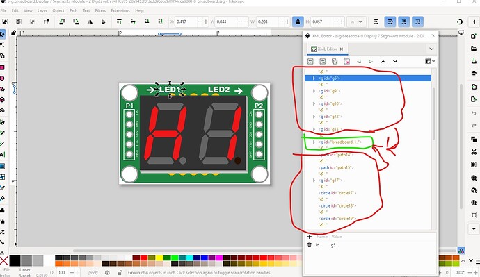
Looking at the breadboard svg, you do in fact have a layerId but it is in the wrong place (it needs to contain all the elements of the part anything outside that group will not export as an image.)
current breadboard svg
corrected breadboard svg (I ungrouped it completely and then did edit->select all then object group and named the group breadboard.)
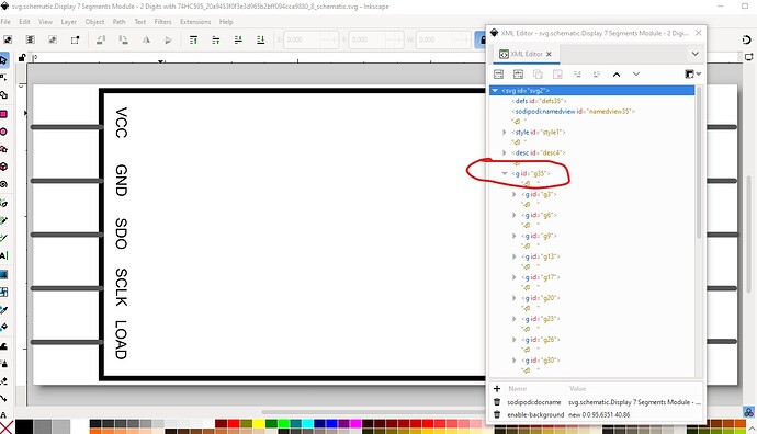
moving on the the schematic svg. It needs a layerId
current svg
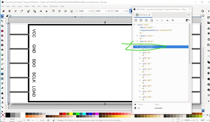
the circled group name needs to be schematic like this:
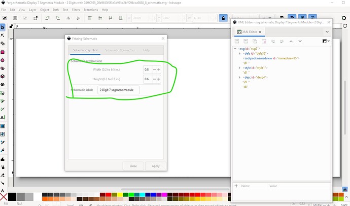
rather than fix the current schematic I chose to use Randy’s schematic Inkscape extension to create a new one (also covered in the tutorial above)
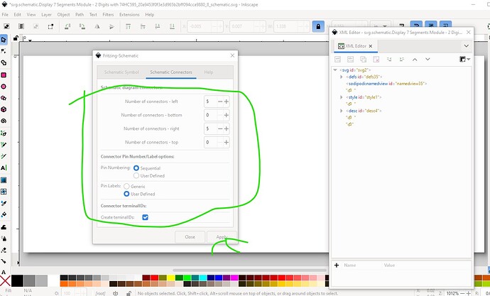
set the parameters and a schematic label
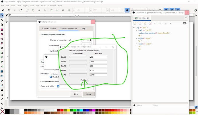
then set the number of pins and hit Apply
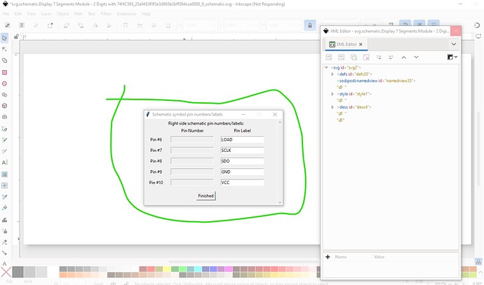
then set the pin labels and click Finished.
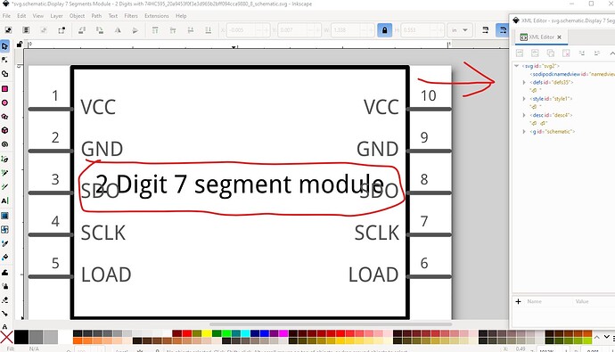
then click finished and it writes a correct shematic svg which meets the graphics standards.
in this case I made the width too short so I need to manually adjust it (I could also re run the extension with a higher width of about 1in.)
on to the pcb svg. You do in fact have pins defined just not the appropriate layerIds and too much text.
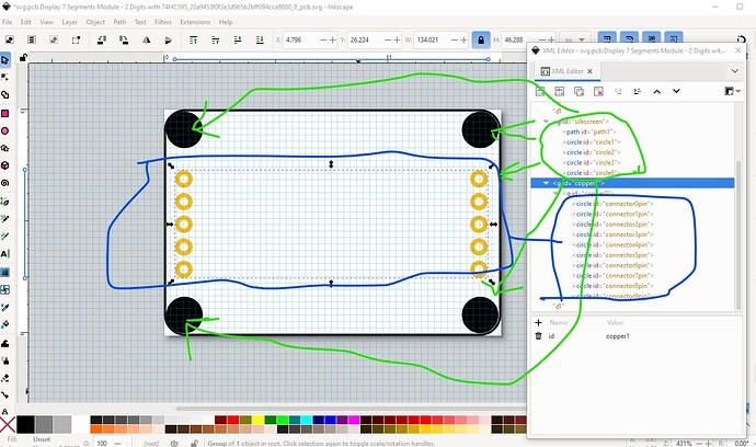
So I changed that to this
Which has pads of a suitable size for 0.1in headers and the board outline and the mounting holes in silkscreen. By default the mounting holes are not drilled, they are only in silkscreen. If you want holes you can drag a hole part in to the sketch over the hole in silkscreen and then set the size appropriately. That way you can have the mounting holes if you want them but don’t have to modify the part to remove them if you don’t want them. I expect I will need to modify the .fzp file to make this happen though but pcb is now done. So on to the .fzp file.
<label>74HC595</label>
needs to become
<label>A</label>
to correct the part label. Then I changed the tyoe from female to male (so the part will connect to a breadboard, female will not!) and removed the terminalId from the breadboard line as it is not needed (and not in the svg.) As the pcb svg has been corrected pcb view will now connect correctly as the connections are correct here.
from
   <connector id="connector0" name="VCC" type="female">
     <description>VCC</description>
     <views>
       <breadboardView>
         <p layer="breadboard" svgId="connector0pin" terminalId="connector0terminal"/>
       </breadboardView>
       <schematicView>
         <p layer="schematic" svgId="connector0pin" terminalId="connector0terminal"/>
       </schematicView>
       <pcbView>
         <p layer="copper0" svgId="connector0pin"/>
         <p layer="copper1" svgId="connector0pin"/>
       </pcbView>
to
    <connector id="connector0" name="VCC" type="male">
      <description>VCC</description>
      <views>
        <breadboardView>
          <p layer="breadboard" svgId="connector0pin"/>
        </breadboardView>
        <schematicView>
          <p layer="schematic" svgId="connector0pin" terminalId="connector0terminal"/>
        </schematicView>
        <pcbView>
          <p layer="copper0" svgId="connector0pin"/>
          <p layer="copper1" svgId="connector0pin"/>
        </pcbView>
at connector4 (and the rest of the way down) I needed to add the terminalId definition so schematic will work correctly.
from
    <connector id="connector4" name="LOAD" type="male">
      <description>LOAD</description>
      <views>
        <breadboardView>
          <p layer="breadboard" svgId="connector4pin"/>
        </breadboardView>
        <schematicView>
          <p layer="schematic" svgId="connector4pin"/>
        </schematicView>
to
    <connector id="connector4" name="LOAD" type="male">
      <description>LOAD</description>
      <views>
        <breadboardView>
          <p layer="breadboard" svgId="connector4pin"/>
        </breadboardView>
        <schematicView>
          <p layer="schematic" svgId="connector4pin" terminalId="connector4terminal"/>
        </schematicView>
        <pcbView>
          <p layer="copper0" svgId="connector4pin"/>
          <p layer="copper1" svgId="connector4pin"/>
        </pcbView>
      </views>
    </connector>
at connector 5 we need to change the description so the pins are in the correct order that Frizting is expecting. That would be
5 load 2
6 sclk 2
7 sdo 2
8 gnd 2
9 VCC 2
I expect the family shouldn’t be “grove” as it is not a grove device (they have 4 pin 2mm grove connectors not 0.1in pads) but I left it as is as it shouldn’t hurt anything. That produces this new improved part which will connect to a breadboard like this: (the other end would need to go to a different breadboard)
where in pcb the pins now connect to the pins on the device. This comes from this part
Display 7 Segments Module - 2 Digits with 74HC595-improved.fzpz (11.2 KB)
note you will need to delete the current part in your mine parts bin, then shut down Fritzing saying yes to save parts and save mine parts bin, then restart Fritzing before it will let you load the new part as the moduleIds are the same. Hope this helps.
Peter
