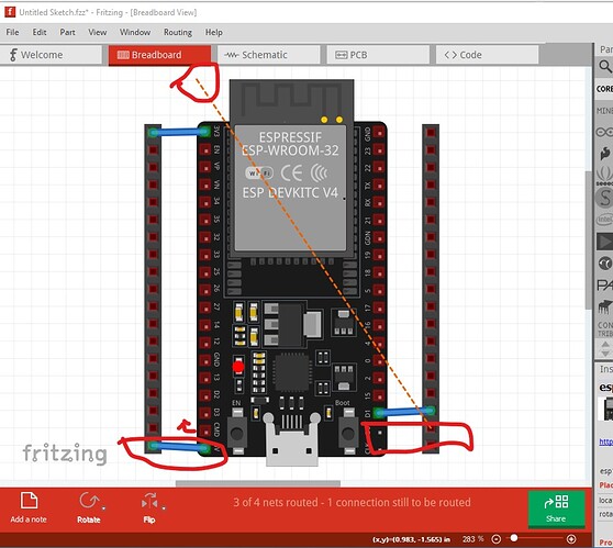
Not a bad job, but a number of errors. This tutorial set should tell you how to correct them:
Starting in breadboard
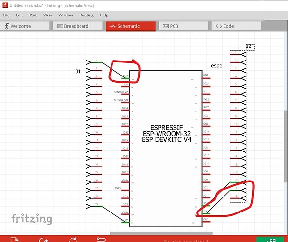
The scale is slightly wrong. Note the bottom left wire is not straight. The pins should be exactly on a 0.1in boundary and they are not. You likely need to rescale the image slightly to correct this. The bottom two right connectors are not correctly defined and thus don’t connect. The ratsnest line comes from this connection in schematic (which is almost correct other than the terminalIds)
The wires are connecting to the center of the pin because the terminalIds are not correct (missing completely in some cases.) The fzp file should look like this:
<breadboardView>
   <p layer="breadboard" legId="connector1leg" svgId="connector1pin"/>
  </breadboardView>
<schematicView>
   <p terminalId="connector1terminal" layer="schematic" svgId="connector1pin"/>
  </schematicView>
<pcbView>
   <p layer="copper0" svgId="connector1pin"/>
   <p layer="copper1" svgId="connector1pin"/>
</pcbView>
where each connector has a terminalId called connectorxterminal which is also in the schematic svg. In the current fzp file many of the pins lack the terminalId definition causing the above problem.
<breadboardView>
  <p layer="breadboard" svgId="connector3pin"/>
</breadboardView>
<schematicView>
  <p layer="schematic" svgId="connector3pin"/>
</schematicView>
<pcbView>
  <p layer="copper0" svgId="connector3pin"/>
  <p layer="copper1" svgId="connector3pin"/>
</pcbView>
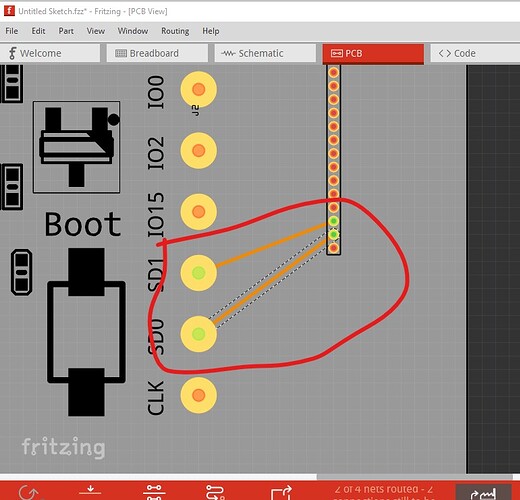
there should be a terminalId=“connector3terminal” added to the schematic connector entry above. The pcb svg is the wrong scale. The pins on the board should be in the same place as the header beside it as one is supposed to connect to the other.
the traces should be horizontal not at an angle. If you have troubles fixing this feel free to ask for help!
Peter


