Fritzing-Schematic an Inkscape extension - released

Well I guess I didn’t test it enough prior! I had forgotten about the zero-referenced terminal/pin gig. But anyway I tested it again and it worked without issue. The issue I prior described about things being out of order or mis-matched was unfounded. Well done - this is really slick.

The advantage is that it is an option. You have a choice, create terminalIds or don’t, and having choices is a good thing. But really, this comes down to a workflow sort of thing. Of all the schematic symbols I’ve created in Inkscape, I never once created terminalIds. It’s too much work in Inkscape to add them, when it can be done in the parts editor with a couple of mouse clicks. Originally, I wasn’t even going to add the creation of terminalIds, but it wasn’t much work to add them in and made the tool more robust.

I think Peter explained this well, but just let me say that this is the way of Fritzing. In Fritzing, grab a Generic IC and drag it into the schematic view, or any view, doesn’t really matter. Edit the part in the parts editor, and choose the Connectors tab. You should see something like this:


Notice how pin1 has an id of connector0. connector0 is the connector0pin in the .svg

Anyhow, I’ll update some info here soon!
Randy

1 Like

An update:

Thanks to @vanepp for discovering a small bug in my extension! Basically, if the symbol size is too small and you try to create too many connectors for the bottom, right, or top side of the symbol, the extension will fail. The code has been updated on github.

So head over here:
https://github.com/revolt-randy/Fritzing-Schematic-an-Inkscape-Extension. (same link as first post) and grab the latest update.

Randy

1 Like

I cannot download anything there, please give instructions for stupid engineers over 75.
Bill

Yes it is a little unusual. You need to select change the display to raw from this

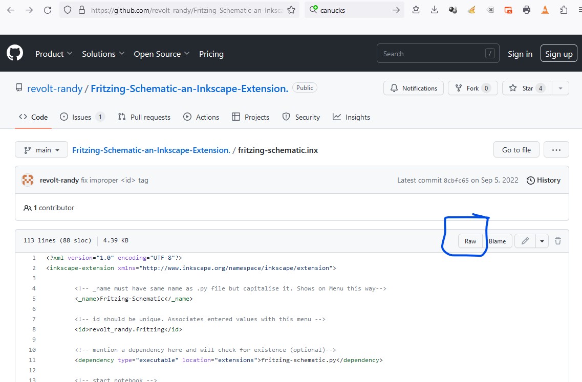
by clicking the raw button (circled in blue) to remove the line numbers and leave the raw file like this

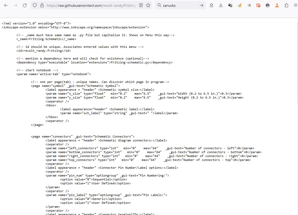
then (at least in firefox!) right click and click select all to select the entire text.

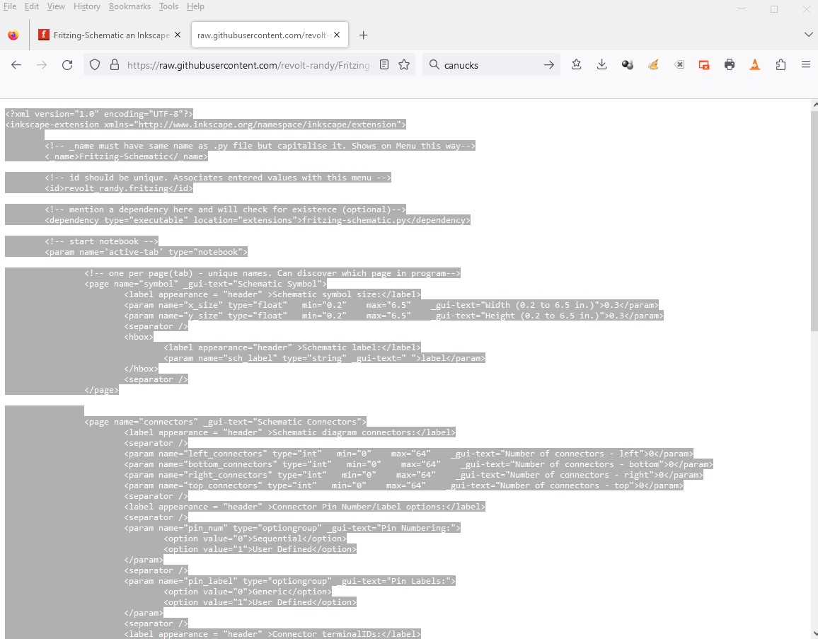
then copy the text and paste it in to a file called fritzing-schematic.inx by pasting the text in to the editor and then saving the file. Repeat with the
fritzing-schematic.py file. Then you need to copy both files in to the Inkscape extensions folder like this:

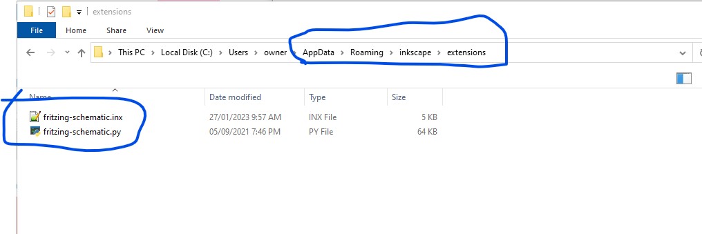
note this is on Windows10 and the AppData directory is a hidden directory so you need to enable display hidden files in Explorer in order to see the directory.

edit:

As you appear to be looking at making parts, these tutorial series may help. Old_grey uses the parts editor and video tutorials, mine are text and don’t use parts editor.

as well part 10 of my series covers Randy’s schematic extension (which I use pretty much exclusively now.) I don’t think I was quite as detailed about how to get the files off of github though.

Peter

Got It, thanks… now to find out if I have to do anything special to USE it.
Thanks again
Bill

It is reasonably simple, but somewhat fixed. By default it starts on the left side with connector0 and goes (increasing one pin at a time) from there to bottom then right then top. You can also specify custom pins by ticking a box (at which point you need to enter both the pin number and the name). That means you need to think about how you want to layout schematic to get the pins in the correct place. The section of the tutorial on using it may help too. I usually start in breadboard and move the pins around so they will be in the correct sequence for the schematic extension, and often end up doing schematic more than once when I forget something.

Peter

@vanepp & @BillRedd

When I go to the extension on github I get this screen:

and clicking on the green ‘Code’ button brings up a popup that allows me to select an option to ‘Download ZIP’ to download all files as a .zip file.

Are you guys not seeing that option?

Randy

Its there I just didn’t know what it did and tried to access the file by clicking on the file name (circled in red here) which doesn’t offer a download operation.

If I click the code button, it does indeed offer the option of downloading a zip (but as usual with github in a non intuitive way.)

Thanks, now I know what to do in similar cases. Usually clicking on the file will bring up a download option, but in this case it doesn’t and I have been using the copy to the clip board and save in a file method to get such files. Now I know to click the code button instead.

Peter

Okay, I updated the README.md file on github, adding in download instructions

It appears I cannot edit my first post to add in download instructions, so I’ll add that info here.

On the github page for this extension, look for the green button ‘Code’:

Clicking on that button will bring up a popup menu:

Select the ‘Download ZIP’ option to start a download of all files. Once the .zip file is downloaded, copy the two required files to Inkscape’s extensions directory. Additionally, all three files could be un-zipped to Inkscape’s extensions directory. Inkscape should ignore the ‘README.md’ file. (not tested)

Hope this helps,
Randy

Hi, Do you have any plans for making an extension for PCB svg??
Personally, I feel PCB SVG is the most complicated thing to make.
Do you know of any extensions or anyone who is working on an extension to make PCB svgs??

While I’m not Randy (the author of this extension) I helped him develop it. Unfortunately breadboard and pcb are not as easy to arrange as schematic (where the pin sizes and positions are more or less fixed) so I doubt a plug in for either of them are possible. This tutorial series may help you, as it covers what you need to do in pcb and what the groups need to look like. Unfortunately it isn’t simple and it isn’t too likely to become so (although there is work ongoing on parts editor now.)

Peter

Hello, Vanepp. I had gone through both the tutorials you have mentioned and a few others. Personally, I found Jacob fenwik’s tutorial easiest to get good results with.

http://jacobfenwick.com/making-a-part-in-fritzing-0-8-7b/

Here’s my idea of what the best case scenario would be for PCB schematics of parts. This might be extremely difficult to implement and/or might have a lot of other shortfalls, but if it was possible, it would be a dream.

Use LibreCAD or Qcad or Autocad/Inventor/Solidworks/Fusion/BRL-CAD or any other CAD program to create the footprint of the PCB, export it as an SVG and import the SVG into Fritzing. No need of constantly fiddling about with the layers/groups. Just get the SVG into fritzing, use fritzing’s GUI to pick and select each line/circle/rectangle basically any element and define it’s purpose in the PCB view of fritzing parts editor.

What I have found to be extremely annoying with inkscape is that the measurements of circles are taken from the corner of the bounding box and not the centre. This makes placing circles a P.I.T.A. Engineers and Tinkerers are extremely used to CAD softwares. There are a lot of FOSS cad programmes out there, which can be used to create a DXF/SVG file.

Finally, I found that editing existing working parts is the best option. DO NOT try to create an svg from scratch using cad right now. Fritzing needs Groups and layers and stuff. Even those groups should be in a very particular way for it to work(so creating a new SVG in Inkscape following grouping and layering rules is also not going to end well. It is TOOOOO finicky).

If anyone needs, I was making parts of EASYPOWER’s power supply modules(5V and 24V models).
I am attaching them here.
SO5V1000.fzpz (8.2 KB)
SO24V500.fzpz (8.6 KB)

Your SO5V1000 part has a number of problems. I ran it through FritzingCheckPart.py which flagged the following errors (there are a bunch of warnings as well, but the errors are by and large the important part):

Error 18: File
‘part.EasyPower_SO5V1000_8f2806aad67f3da3bb87188cc02b299f_1.fzp.bak’

Connector connector0terminal is in the fzp file but not the svg file. (typo?)

svg svg.breadboard.EasyPower_SO5V1000_926589be4af404b0a68a8a53c88a64f9_2_breadboard.svg.bak

Error 18: File
‘part.EasyPower_SO5V1000_8f2806aad67f3da3bb87188cc02b299f_1.fzp.bak’

Connector connector2terminal is in the fzp file but not the svg file. (typo?)

svg svg.breadboard.EasyPower_SO5V1000_926589be4af404b0a68a8a53c88a64f9_2_breadboard.svg.bak

Error 18: File
‘part.EasyPower_SO5V1000_8f2806aad67f3da3bb87188cc02b299f_1.fzp.bak’

Connector connector3terminal is in the fzp file but not the svg file. (typo?)

svg svg.breadboard.EasyPower_SO5V1000_926589be4af404b0a68a8a53c88a64f9_2_breadboard.svg.bak

Error 69: File
‘svg.schematic.EasyPower_SO5V1000_926589be4af404b0a68a8a53c88a64f9_2_schematic.svg.bak’
At line 27

Found a drawing element before a layerId (or no layerId)

Error 65: File
‘svg.pcb.EasyPower_SO5V1000_926589be4af404b0a68a8a53c88a64f9_2_pcb.svg.bak’
At line 52

Connector connector2pin is an ellipse not a circle, (gerber generation will break.)

Error 74: File
‘svg.pcb.EasyPower_SO5V1000_926589be4af404b0a68a8a53c88a64f9_2_pcb.svg.bak’
At line 52

Connector connector2pin has no radius no hole will be generated

Error 65: File
‘svg.pcb.EasyPower_SO5V1000_926589be4af404b0a68a8a53c88a64f9_2_pcb.svg.bak’
At line 53

Connector connector1pin is an ellipse not a circle, (gerber generation will break.)

Error 74: File
‘svg.pcb.EasyPower_SO5V1000_926589be4af404b0a68a8a53c88a64f9_2_pcb.svg.bak’
At line 53

Connector connector1pin has no radius no hole will be generated

Error 65: File
‘svg.pcb.EasyPower_SO5V1000_926589be4af404b0a68a8a53c88a64f9_2_pcb.svg.bak’
At line 54

Connector connector3pin is an ellipse not a circle, (gerber generation will break.)

Error 74: File
‘svg.pcb.EasyPower_SO5V1000_926589be4af404b0a68a8a53c88a64f9_2_pcb.svg.bak’
At line 54

Connector connector3pin has no radius no hole will be generated

Error 65: File
‘svg.pcb.EasyPower_SO5V1000_926589be4af404b0a68a8a53c88a64f9_2_pcb.svg.bak’
At line 55

Connector connector0pin is an ellipse not a circle, (gerber generation will break.)

Error 74: File
‘svg.pcb.EasyPower_SO5V1000_926589be4af404b0a68a8a53c88a64f9_2_pcb.svg.bak’
At line 55

Connector connector0pin has no radius no hole will be generated

The no radius errors are because the pcb svg is incorrect and thus won’t (and doesn’t) create proper gerber files.

This is because the pcb svg needs to have a copper0 group as a child of the copper1 group and the pads need to be circles not ellipses as they currently are:

needs to change to look like this:

all the silkscreen elements are in a group labeled silkscreen (which needs to match the layerId in the fzp file) and the connectors are circles in group copper1 which contains group copper0 which contains the pads. This will export correctly to the gerber output to make boards. You also need to set the hole size to an appropriate value (the data sheet for this part doesn’t have enough information to tell what the hole size should be, so I would default to 0.038in which is the size to take a 0.1 header pin. With the current pcb svg you can only route traces on the top of the board (because only copper1 is defined.) Schematic you would be better to run Randy’s Inkscape extension because it will do this correctly automatically, but your current schematic is not correctly aligned to the grid:

The two pins circled in red need to move back a bit to align to the 0.1in grid lines. There are also standards for the color of the text (which the extension obeys.) Making correct parts is without a doubt complex, but to successfully make parts you need to understand all the things that need to be done. As well it is not correct that you can’t make parts from scratch, I do it regularly. That limitation is because parts editor was not finished when development stopped and parts editor has limitations on what can be changed (for instance you can not change the number of pins defined in the fzp file in parts editor AFAIK.) That is where the requirement that you start from an existing part (which is a good idea anyway even if you know what you are doing as it is less work!) comes from. If you don’t use the parts editor (which I normally do not) that isn’t a problem. The warning about missing layerId means the part will not be exported as an image (svg, jpg etc.)

Peter

Wow! That was a lot of errors.
I am currently focusing only on getting the PCB footprint correct for manufacturing, so I kinda let the breadboard port names be whatever they wanted to be. But seeing the later errors, I realise tehre might be problems with the PCB manufacture. I will need to look into this issue. I will fix the parts and will re-post them here as soon as I am done rectifying them.

the pads need to be circles not ellipses as they currently are:

Can you please tell me how to convert an ellipse element into a circle element? Currently I have found wrangling inkscape to be a bigger challenge than designing the entire project.

How to edit the fzp file to change the connector names to match the PCB svg file?
I have a total of 5 parts that I made which are all required for my design. Unfortunately, I am guessing none of them will work well when gerber exporting the design made in PCB mode since the connectors made by me look different.


See the difference in the pin? The LED is a standard component. The connector pads are golden with red filled in circles. Mine are golden with red hollow circles inside. Does that mean my part will not export as gerber?
I don’t really care much about the schematic mode lining up with the grid. I am only bothered about PCB mode. If the PCB cannot export to gerber, the manufacturer cannot make it.

Could someone please please please make a plugin or something that converts DXF/DWG files to fritzing parts? I can easily make a PCB footprint in CAD. But fritzing will not accept that.
At least a python script that will create the SVG file with recommended layers and names and connection points based on a coordinate system that I enter? I can envision something like a CSV file being imported into python. The script will open the file, create the sbg based off of the details in the CSV. example csv attached for reference(rename the file to remove fzp at the end).


example_file - Copy.xlsx.fzp (10.4 KB)

Using the pcb svg file svg.pcb.EasyPower_SO5V1000_926589be4af404b0a68a8a53c88a64f9_2_pcb.svg from the SO5V1000 part, do this:

These three values need to change (note I rescaled the svg to be the correct 1 drawing unit = 1 thousandth of an inch to make this easier.) rx and ry need to change to 29 (to make a 0.038in hole for a 0.1in header.) The stroke-width needs to change to 20 to make a 20 thou ring. The hole diameter in Inkscape will be

hole_diameter = pad_diameter - (2 x stroke-width)

in this case that will be .038in as the pad diameter is 0.078in and the stroke-width is 0.02in.

Changing the rx and ry is however not enough (Inkscape quirk!) now you need to move the pad to cause Inkscape to recognize it has changed from an ellipse to a circle and reset it.

to have only a radius (r) like this.

as a side issue, you need to increase the font size of your text like this

then you need to regroup the parts in to the appropriate groups like this:

which results in this corrected svg:

svg.pcb.EasyPower_SO5V1000_926589be4af404b0a68a8a53c88a64f9_2_pcb

(right click and save image as to download the svg.)

edit part.EasyPower_SO5V1000_8f2806aad67f3da3bb87188cc02b299f_1.fzp with a text editor, then adjust the xml for the connectors as needed:

    <connector id="connector0" type="male" name="AC">
      <description>AC</description>
      <views>
        <breadboardView>
          <p layer="breadboard" svgId="connector0pin" terminalId="connector0terminal"/>
        </breadboardView>
        <schematicView>
          <p layer="schematic" svgId="connector0pin" terminalId="connector0terminal"/>
        </schematicView>
        <pcbView>
          <p layer="copper0" svgId="connector0pin"/>
          <p layer="copper1" svgId="connector0pin"/>
        </pcbView>
      </views>
    </connector>

the pin numbers are in the xml as connector0pin in this case, change as needed then save the fzp file.

The likely difference is stroke-width. The standard value is 20 thou, if you use larger as you appear to here they will be larger but as long as the circles are circles, will export correctly. However note gerber processing takes place after the pcb render so although it looks fine in pcb view that does not mean the gerber is correct. You need to display the gerber output with a gerber viewer (I use gerbv from the gEDA project, but there are lots of them) to make sure the gerbers are correct.

As noted I expect that won’t be easy and to my knowledge isn’t being considered. There is development work occurring on parts editor but it isn’t finished nor released yet nor do I know what all the aims are.

Peter

Hi Peter, Thank you for all your time and effort.
Could you please elaborate on:

note I rescaled the svg to be the correct 1 drawing unit = 1 thousandth of an inch to make this easier.

Regarding the font, my Inkscape does not look like that at all.
mine looks like this and they both say fontsize = 6px.


but the gerber looks like this:

I also tried seeing the font size of the group that was hiding the text. They both show different sizes(all groups do the same thing. GND, AC, 5V).


My inkscape does not show Font family also like yours does.

Thanks for this formula

hole_diameter = pad_diameter - (2 x stroke-width)

I used the other end. I found

StrokeWidth is the ring thickness. So, if I know how thick I need the ring around my component to be,
required circle radius = holeRadius + (StrokeWidth/2)
ex: I need a 1mm-dia hole and a 0.5mm ring around it. So, strokeWidth = 0.5, circleRadius = 0.5+(0.5/2) = 0.75

I tried making Rx and Ry the same but did not know that moving it a bit will change it from ellipse to circle. Thanks for the tip. I exported my old parts to gerber. Holes were not drilled. I then deleted all my connectors, re-created new connectors using circles and pressing and holding Ctrl whilst dragging out the circle.
This time, I also made Copper0 subgroup inside copper1 group and placed all the connectors inside it(in the inner group, copper0).
The PCBview connectors are displayed correctly and The gerber worked perfectly(holes and all).
So, things I have noticed in order to make gerber work properly and drill points to exist, there need to be:

  • Two copper layers (with all connector pads inside copper0 which is inside copper1)
  • Circles instead of ellipses

I still do not understand the following:

  • The need for the schematic to be perfectly aligned with the grid. Is the schematic used for anything other than reference? Do any programs(kiCad or eagle) use it?
  • The need for the TerminalID to match the connectorID?
  • how to make my silkscreen text uniform?

For the time-being though, my purpose is being served. I am able to create a usable PCB with a true footprint and accurate hole positioning. I would like to get better at this though. If I can, I’ll make that programme I was talking to you about. I’ll definitely share it with everyone if I can get it working. Thanks for pointing me to gEDA suite. Thanks again for being so patient.