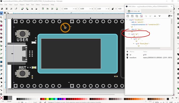
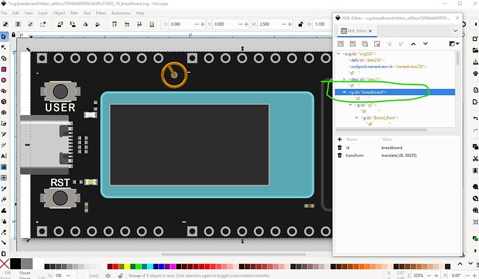
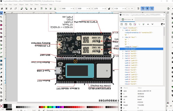
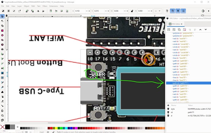
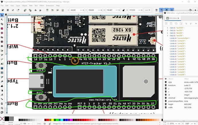
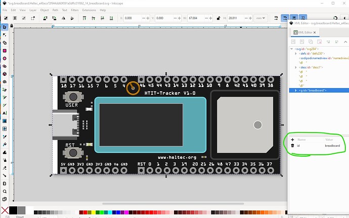
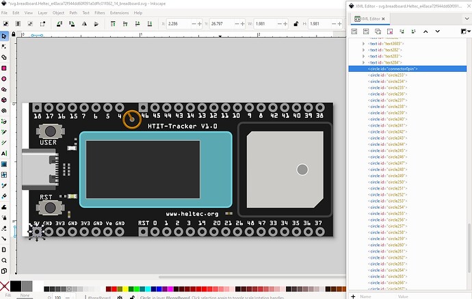
There isn’t very much wrong with your part. As you said the pin spacing is a little off but over all the part works fairly well as it. The first issue is that breadboard doesn’t have a layerId. As a result your part in a sketch will not export as an image (that is the only thing I know this affects but there may be others as well.) It needs to match the layerId in the .fzp file for the part which will usually be “breadboard” and be the top layer group that contains the entire svg
original svg
corrected
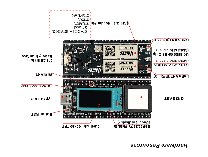
Then I looked over the breadboard svg (I’m using Inkscape here, it looks like you are using Illustrator?) The first thing I did was grab this png from the heltec site and imported it in to Inkscape
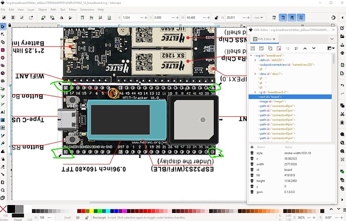
then scaled the png so the pins matched the connector on the board.
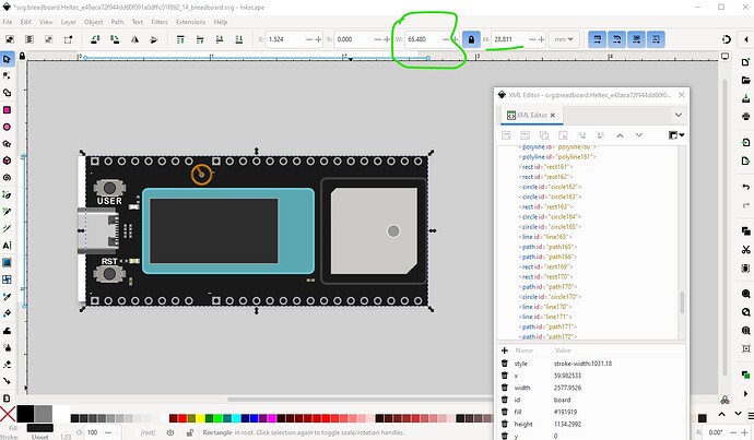
I actually sized it via a 25 pin male header from Fritzing which will be the exact correct length. The I selected just the board, locked height and width then set the size to 65.48 mm (as the listed size on the Heltec web site.) That make the board a little long to the listed length, but I left it alone because it better matched the size of the image.
Then I created a standard header pad that matches the Fritzing 0.1in header definition
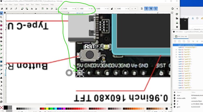
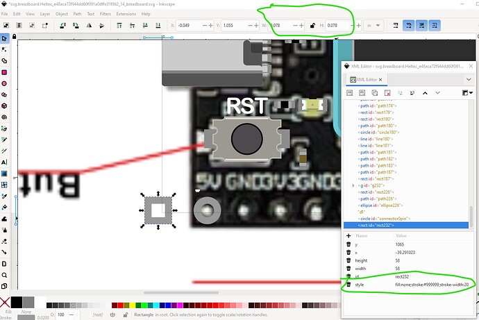
then moved that to near the bottom left connector (which by Fritzing convention is connector0pin.) I selected the current pad at that position and noted its its x and y coordinates
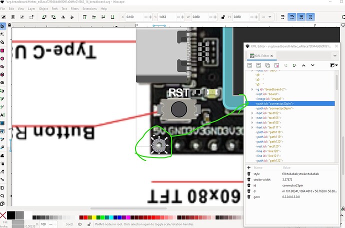
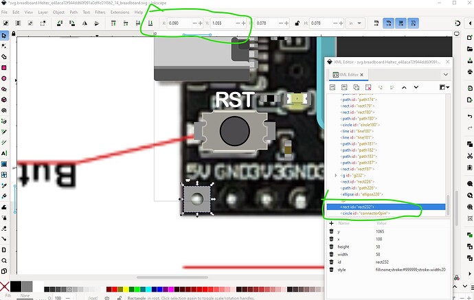
then I moved the new pad to the same position as the original pad like this
and deleted the old pad and added the square that is on this pin.
and moved it on top of the connector.
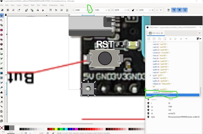
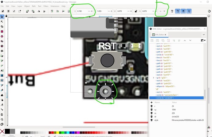
Then I selected the circle that is the pad and duplicated it then clicked the + tab on the x icon to move the pad 0.1in in x
this is the easiest way I know in Inkscape to correctly space connectors (at least 0.1in connector!) You can also do so by adding the appropriate increment to the x coord and then copying the new value in to the x coord (useful for 2mm connectors!)
then ,move on to the connectors on the top
now replace the text rendered as paths with text (as it is easier to modify if you or someone else needs to modify the part!)
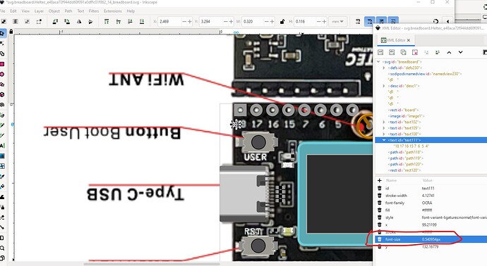
The labels for the pins are set as text (desirable) but have had their font size (likely by Fritzing because the px was left on the font size which Fritzing reacts badly to!) reduced to very small so set a larger font size to recover the text.
now we are done so set the layerId by selecting the entire svg and grouping it
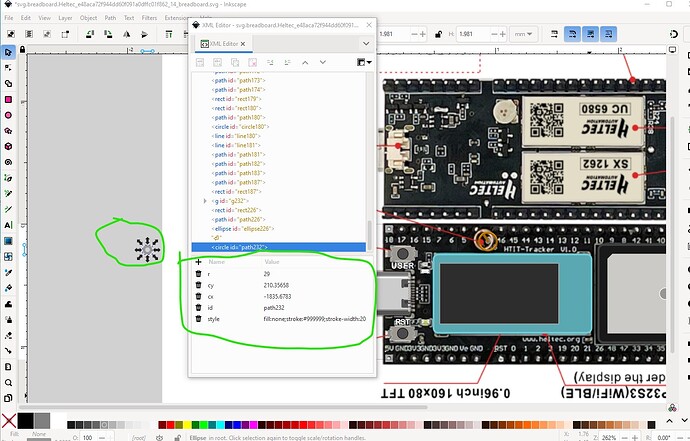
then set the first connector to connector0pin with all the pins being after that at the bottom of the svg. The reason for this is that I have a script which will read the svg and renumber the pins in sequence (laziness at work!) The output from the script looks like this
I then used Randy’s Inkscape extension to create a Fritzing schematic svg for the board, then copied the breadboard svg in to pcb, and edited it to delete all the unneeded components and text and made the appropriate groups for pcb. I then created a .fzp file and labeled the pins then added buses for internally connected pins which resulted in this part which implements the board.
HeltecWirelessTracker.fzpz (13.3 KB)
Pretty much everything I did here is covered in this tutorial (if you haven’t already seen it)
Hopefully I haven’t scared you off and we will see more parts from you ![]() .
.
Peter
