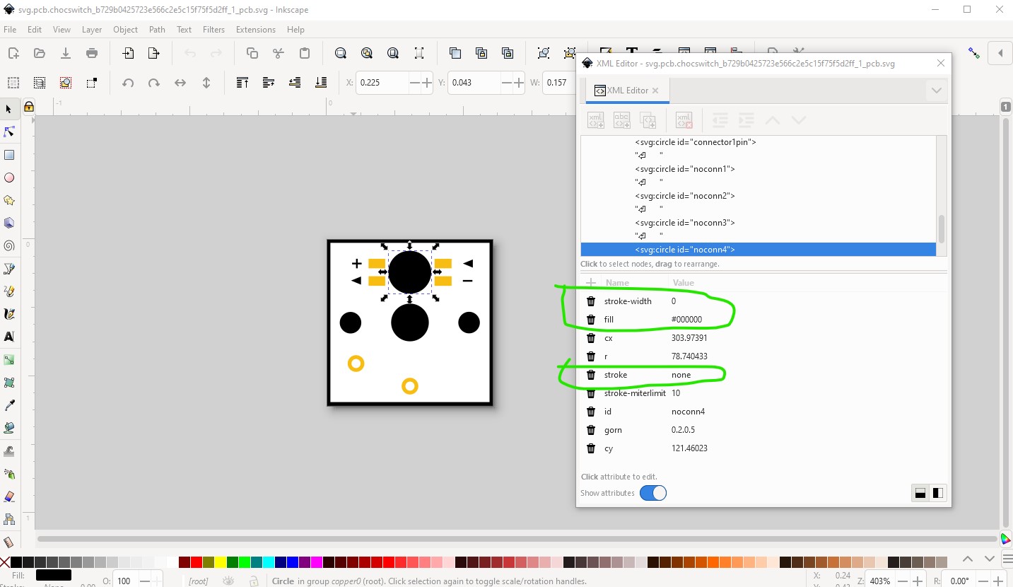
OK, so it looks like you need to swap copper 0 and copper1 in my pcb svg to get the placement right. In the original pcb svg, by the time the nonconns made the svg they had a stroke width (which causes the copper ring):
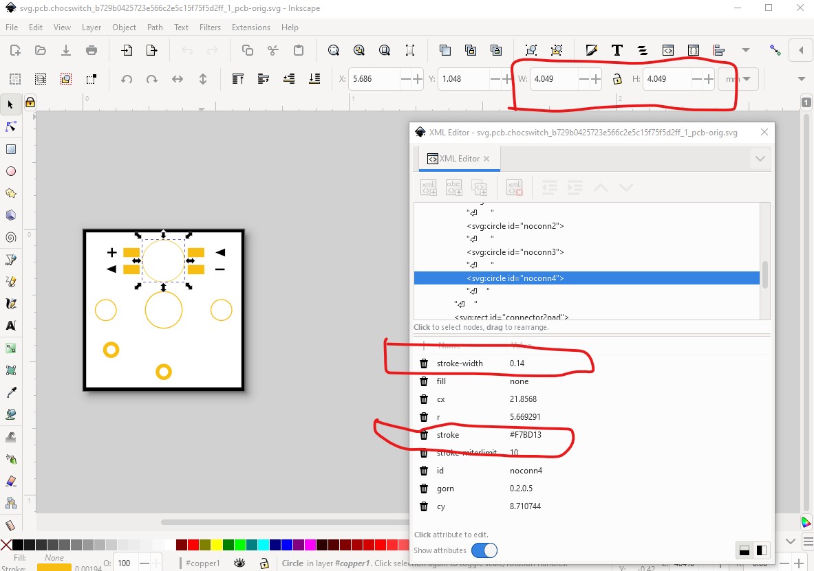
a Fritzing nonconn should have 0 stroke-width and a black fill to drill only the hole like this (I think it actually creates the copper pad as well, but the copper gets removed in the drill stage.)
How I make parts is detailed in this tutorial (which edits the underlying files directly)
old_grey uses parts editor in his tutorials though
(both of these apply to 0.9.10 as well, many of the others are for older versions.) I rarely use parts editor (it is as of 0.9.10 incomplete, I believe it is being worked on) and will likely break with this non standard layout (a mixed through hole and SMD part will likely confuse it!)
It will select the through hole pad on connector0 from the window
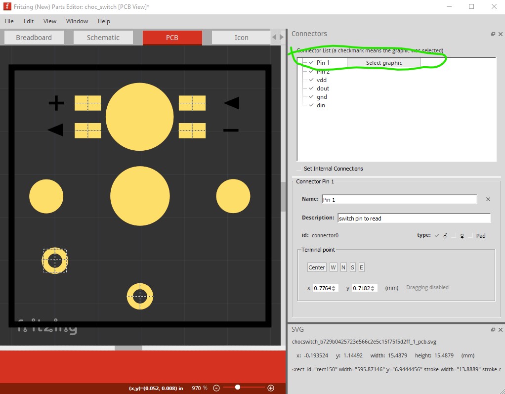
but can’t seem to select the pads only on copper1 unless I click on the label in the connector window (which won’t work I expect if you don’t have the connectors defined.) I expect but don’t know for sure that this is because of the non standard layout of the part.
edit: Slots can not be created in parts, you need to load a custom cutout svg (which are typically difficult to make!) for the entire board which means the slots for all the keys would need to be done in the svg and then the parts moved over them which is a major pain. The usual solution is to use a hole as you have done and that will be much easier in this case. You might want to add a description field to the .fzp file (or description in parts editor) explaining this par is really two parts connected together and give the urls to the individual parts so someone coming on the part knows there isn’t a single part that will do this out there somewhere and can get the two parts and make the part. This should create fairly cool keyboards!
Peter