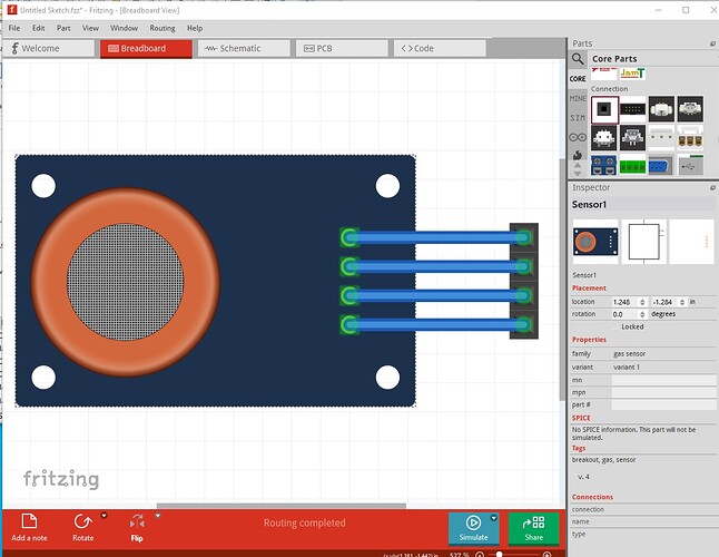
A number of problems in this part. Breadboard lacks a layerId which will cause the part to not export as an image but otherwise looks fine.
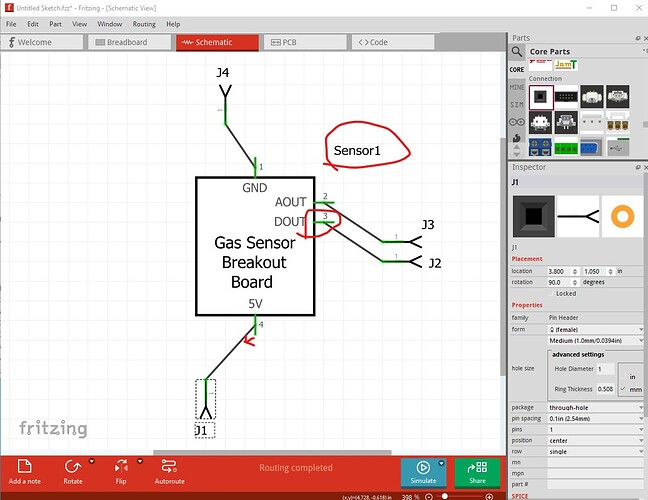
schematic has more issues
It is not correctly aligned to 0.1in boundaries and the terminalIds are groups which won’t work (and thus the wires connect to the middle of the pin as shown above) and last the label in the fzp file should be “A” (for assembly) not Sensor although either will work. FritzingCheckPart.py (which can be found in this part making tutorial)
flags these errors (among others):
Warning 36: File
‘part.mq135_85048d142bf533cdc0527dc579f8434f_1.fzp.bak’
Connector0 doesn’t exist. Connectors should start at 0
Warning 35: File
‘part.mq135_85048d142bf533cdc0527dc579f8434f_1.fzp.bak’
Connector0 doesn’t exist when it must to stay in sequence
In Fritzing connectors should start at connector0 not connector1.
Error 69: File
‘svg.breadboard.mq135_85048d142bf533cdc0527dc579f8434f_1_breadboard.svg.bak’
At line 8
Found a drawing element before a layerId (or no layerId)
indicating the breadboard svg should have the entire svg enclosed in a group labeled “breadboard” to export as an image.
Error 77: File
‘svg.schematic.mq135_85048d142bf533cdc0527dc579f8434f_1_schematic.svg.bak’
At line 13
terminalId connector11terminal can’t be a g as it won’t work.
Error 77: File
‘svg.schematic.mq135_85048d142bf533cdc0527dc579f8434f_1_schematic.svg.bak’
At line 17
terminalId connector8terminal can’t be a g as it won’t work.
Error 77: File
‘svg.schematic.mq135_85048d142bf533cdc0527dc579f8434f_1_schematic.svg.bak’
At line 21
terminalId connector9terminal can’t be a g as it won’t work.
Error 77: File
‘svg.schematic.mq135_85048d142bf533cdc0527dc579f8434f_1_schematic.svg.bak’
At line 25
terminalId connector10terminal can’t be a g as it won’t work.
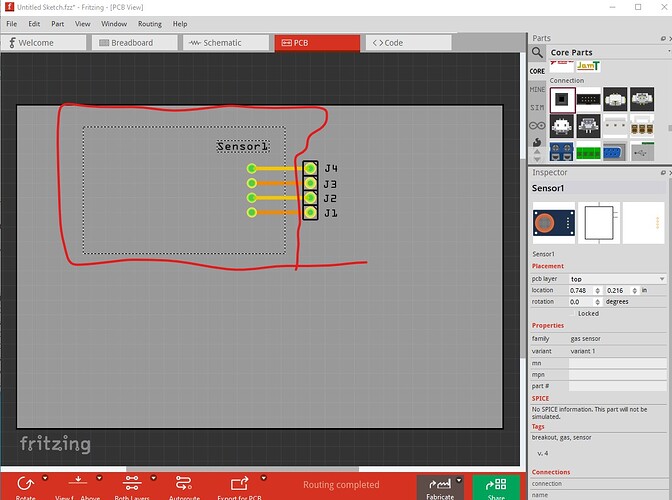
the terminalIds as a group (they need to be a rectangle or other drawing element.) The easiest way to fix schematic is to use Randy’s Inkscape Fritzing schematic extension (assuming you are using Inkscape!) which is detailed in the tutorial. In pcb silkscreen looks to be inncorrect. The box circled in red should be a black box indicating the outline of the board but doesn’t render.
in addition the pads are the incorrect size. They should be 0.038in (for 0.1in headers) not 0.041389. This is the gerber output from the drill.txt file which specifies the hole sizes. As you see the board holes are not the correct 0.038in as the header holes are. How to correct this is also in the tutorial (again assuming you are using Inkscape as I think it is different in other svg editors!)
; NON-PLATED HOLES START AT T1
; THROUGH (PLATED) HOLES START AT T100
M48
INCH
T100C0.041389
T101C0.038000
%
T100
X016117Y017827
X016117Y015827
X016117Y016827
X016117Y014827
T101
X020118Y016827
X020118Y014827
X020118Y015827
X020118Y017827
T00
M30
Hope this helps, if you have questions feel free to post.
Peter


