As you point out the parts work (other than the lack of layerIds causing them to not export as images) so in some sense they are fine. They could be better, but that work may not be worth the effort to you.
Not that I know of at present. There are a lot of things (such as the layerIds) that need to be correct for a part to operate properly. Once you learn the rules making good parts is relatively easy, it does take a lot of time to gain the necessary experience though.
These two sets of tutorials may help:
in my set there is a reference to a schematic template (actually two of them, a simple version and a more complex version) that help with making schematics that meet the standards. At present I usually make schematic using this Inkscape extension as it is easier than the templates, but requires Inkscape (and I see you are using Corel)
Most of the schematic pins have terminalIds except for connector0, and the layerIds are still missing:
Warning 25: File
‘svg.pcb.Tiny RTC I2C module_d6948dd47cb065bc2b9aaa5038e44eed_1_pcb.svg.bak’
At line 243
Silkscreen layer should be above the copper layers for easier selection
in pcb view
Error 69: File
‘svg.breadboard.Tiny RTC I2C module_d6948dd47cb065bc2b9aaa5038e44eed_1_breadboard.svg.bak’
At line 183
Found a drawing element before a layerId (or no layerId)
Error 69: File
‘svg.schematic.Tiny RTC I2C module_d6948dd47cb065bc2b9aaa5038e44eed_1_schematic.svg.bak’
At line 52
Found a drawing element before a layerId (or no layerId)
Error 18: File
‘part.Tiny RTC I2C module.fzp.bak’
Connector connector0terminal is in the fzp file but not the svg file. (typo?)
svg svg.schematic.Tiny RTC I2C module_d6948dd47cb065bc2b9aaa5038e44eed_1_schematic.svg.bak
The lack of a terminalId on connector0 isn’t a problem in this case because connector0pin is at the end of the pin (rather than being the entire pin) and thus the terminalId isn’t really needed. However your part looks somewhat non standard compared to the standard part below it in this image
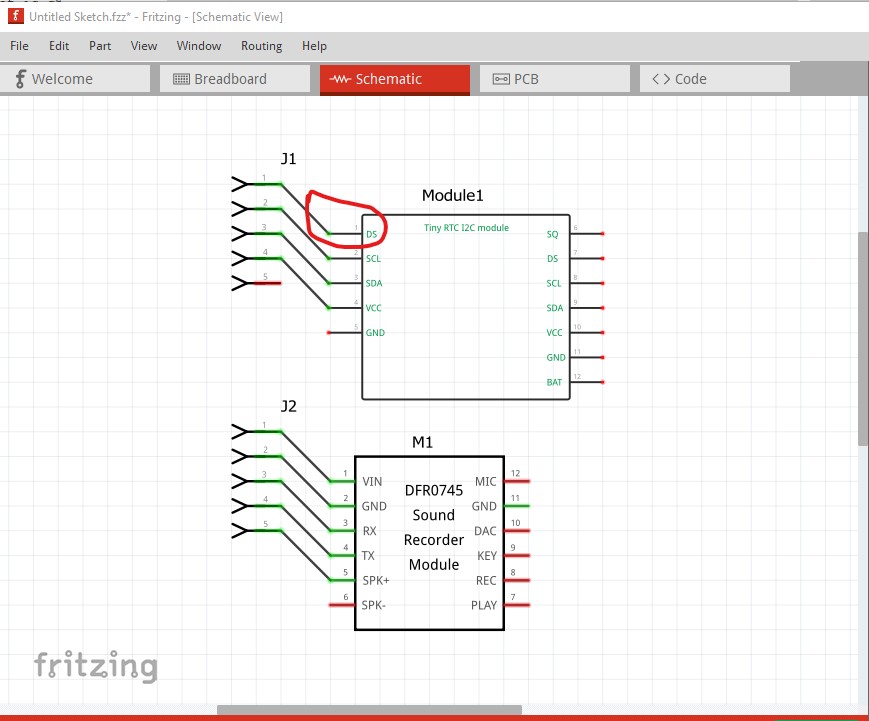
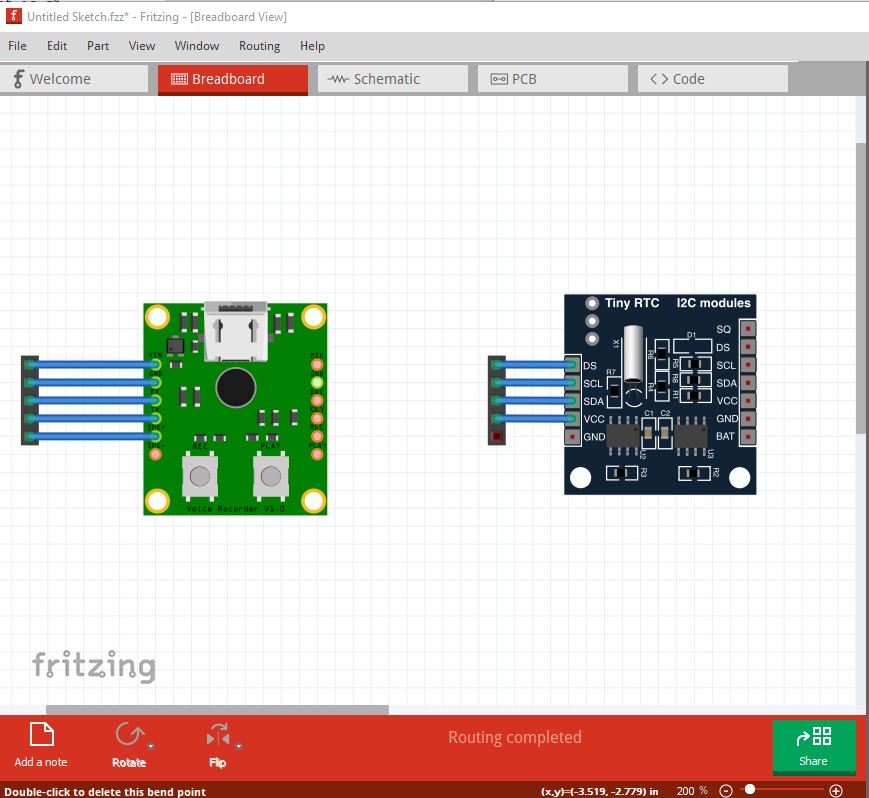
and it is generally desirable that all schematic parts look the same in order to keep schematic looking neat. Here is an example of what the lack of layerId does. This is the image in breadboard view:
and the result of File->export as image->svg and displaying the resulting image in Inkscape:
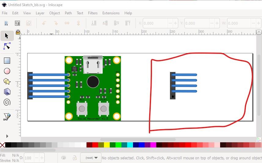
as you see, because of the lack of a layerId the wires to your part are shown but the part itself is missing.
Peter