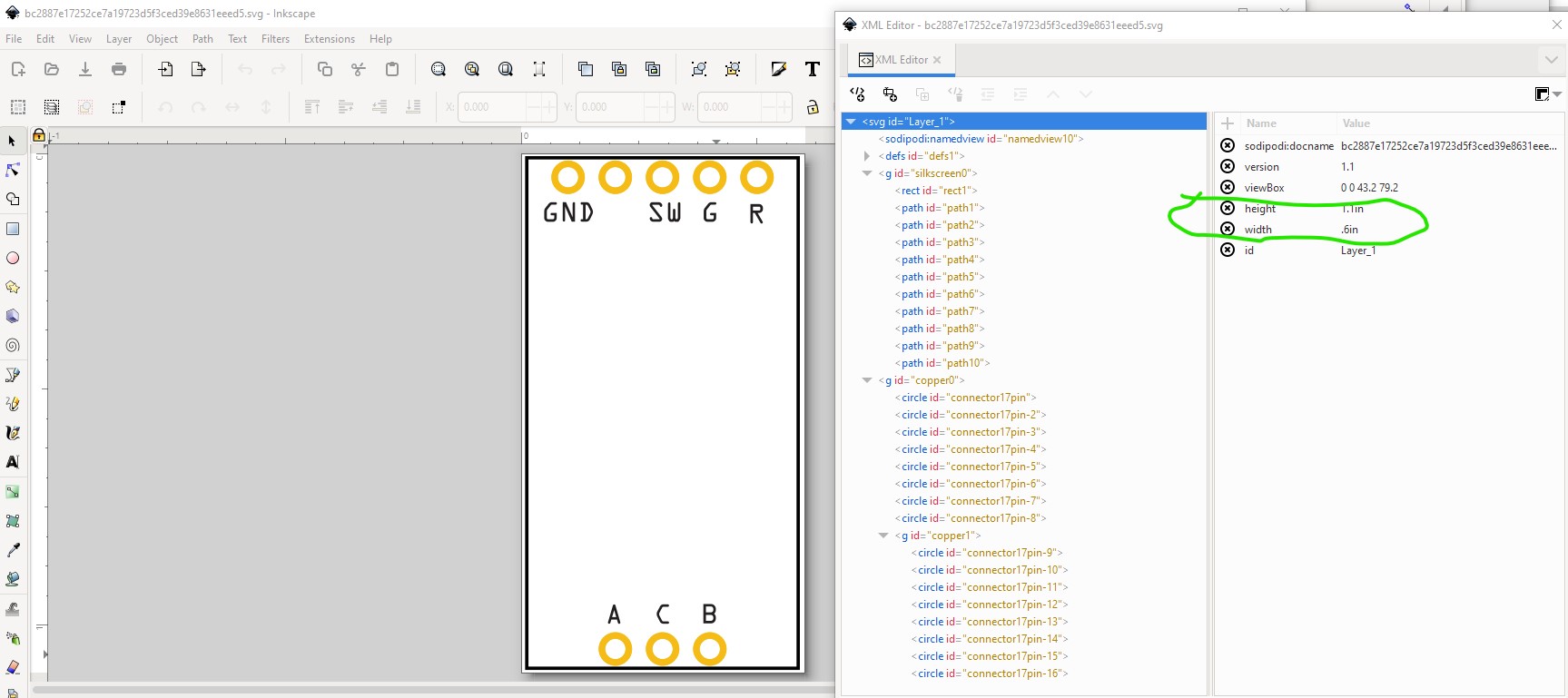
OK, I’m an inkscape user so these displays are from Inkscape but should be reasonably clear. First I have a question (which is of importance to other Illustrator users): do you know what you did to get the dimensions set to in (inches)? Illustrator usually uses px (and I can’t see a way in their documentation to change it!) which causes problems in Fritzing (because Fritzing has to guess what the dpi value is and often gets it wrong which causes scaling problems. )
Be warned, if you can answer this question, I will have others for you ![]() with that unrelated to your question query out of the way, on to what looks to be incorrect in your svg.
with that unrelated to your question query out of the way, on to what looks to be incorrect in your svg.
Almost certainly the .fzp file (the format of which is explained in this part making tutorial set
which should give you a good working knowledge of making parts (I am biased, as I wrote it though ![]() )
)
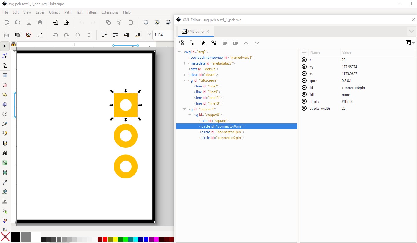
Almost certainly the fzp file has the silkscreen group named silkscreen. Which means (because your group is silkscreen0, you have no silkscreen and thus no outline. Changing the group name to silkscreen should fix that and produce the outline you are expecting. The copper groups are also probably incorrect (and in an old format.) They should look like this:
which is described in the .fzp file like this:
    <pcbView>
      <layers image="pcb/fc-51_85d98481ce3be6f2e9b641181c0f798b_1_pcb.svg">
        <layer layerId="silkscreen"/>
        <layer layerId="copper0"/>
        <layer layerId="copper1"/>
      </layers>
    </pcbView>
  </views>
  <connectors>
    <connector id="connector0" name="pin1" type="male">
      <description>OUT</description>
      <views>
        <breadboardView>
          <p layer="breadboard" svgId="connector0pin" terminalId="connector0terminal"/>
        </breadboardView>
        <schematicView>
          <p layer="schematic" svgId="connector0pin" terminalId="connector0terminal"/>
        </schematicView>
        <pcbView>
          <p layer="copper0" svgId="connector0pin"/>
          <p layer="copper1" svgId="connector0pin"/>
        </pcbView>
      </views>
    </connector>
    <connector id="connector1" name="pin2" type="male">
      <description>GND</description>
Here (as I expect in your .fzp) the layers are the standard silkscreen, copper1 and copper0. The connectors should start at connector0 and increase in sequence one at a time til you are out of connectors. As in the image above copper0 should be a child of copper1 and the connection only defined once (for a through hole part, SMD has only copper1.) To make your current format work correctly both the copper0 and copper1 connector names must match (i.e. both connector0pin) and at least Inkscape won’t let you set duplicate names so you need to edit the svg with at text editor after the svg editor and reset the connector names correctly. That is I expect why the new format was adopted. After that just from the size I expect your holes will be too big. Assuming these are header pins, the hole size needs to be 0.038in and the ring needs to be 20 thousandths of an inch wide. In Inkscape (the other svg editors are likely different) the hole size is
hole-size = pad diameter - (2 x stroke-width)
so with the Inkscape scale set at the desired 1 drawing unit = 1/1000in the diameter needs to be 0.078in to give a 0.038in hole with the noted stroke-width set to 20 (at this scale 20 thou).
Hope this helps, if not feel free to ask further.
Peter