This parts creation tutorial may help. It has pointers to the documentation that exists for the structure of parts and deals with the underlying files rather than parts editor.
Part9 schematic subparts may be of interest as it allows (with a bunch of extra work in making the part!) individual elements of the part to be moved in schematic like this:
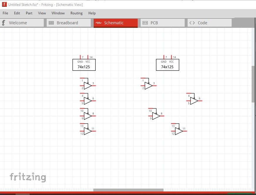
The part on the left is the default but you can click and drag any of the elements as seen on the right individually. This can make logic schematics much more readable.
This should be possible, but I’m guessing you will need to modify the code (which is not easy to understand) to do it. I can give you some pointers to where to look for things though. Every part has a unique moduleId defined in the part’s .fzp file. That is the primary index to everything, so to start you need to have all the parts you need defined (there must be another index value for different instances of the same part though.)
It is output (in the .fz file) as XML like this from this example sketch (the .fzz file):
example.fzz (5.2 KB)
which looks like this:
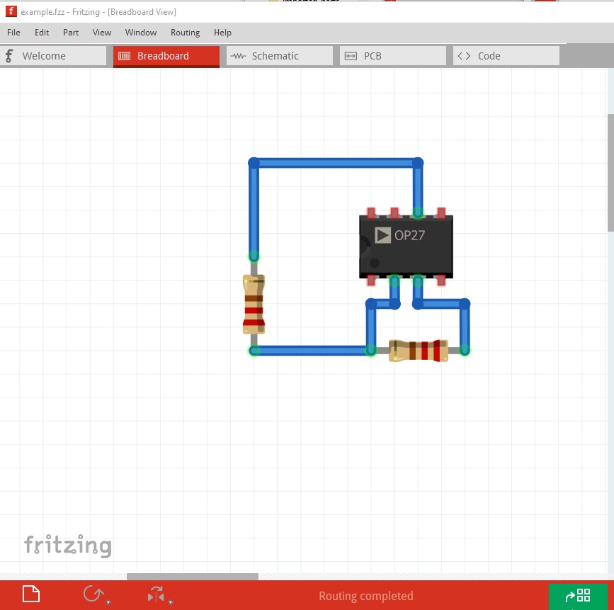
unzipping the .fzz file gives the example.fz file which is the xml which describes the parts and their connections like this:
            <?xml version="1.0" encoding="UTF-8"?>
            <module fritzingVersion="0.9.6b.2021-02-21.CD-175-0-8a1e0682">
                <boards>
                    <board moduleId="TwoLayerRectanglePCBModuleID" title="Rectangular PCB - Resizable" instance="PCB1" width="8.46667cm" height="5.64444cm"/>
                </boards>
                <views>
                    <view name="breadboardView" backgroundColor="#ffffff" gridSize="0.1in" showGrid="1" alignToGrid="1" viewFromBelow="0" colorWiresByLength="0"/>
                    <view name="schematicView" backgroundColor="#ffffff" gridSize="0.1in" showGrid="1" alignToGrid="1" viewFromBelow="0"/>
                    <view name="pcbView" backgroundColor="#333333" gridSize="0.05in" showGrid="1" alignToGrid="1" viewFromBelow="0" autorouteTraceWidth="24"/>
                </views>
                <instances>
                    <instance moduleIdRef="TwoLayerRectanglePCBModuleID" modelIndex="5768" path=":/resources/parts/core/rectangle_pcb_two_layers.fzp">
                        <property name="layers" value="2"/>
                        <property name="width" value="84.66666666666667"/>
                        <property name="height" value="56.44444444444444"/>
I expect the exported netlist is generated from the above XML file (although I’m not sure of that!) Unfortunately the original developers have all left the project and there is very little documentation other than the source code (which is available on github) for how things work and no one who is very familiar with the code.
Assuming the image of the pcb (and hopefully the chips!) is all you have, I think you would need to first create a .fz file with the correct Fritzing parts present and then add the vias in their correct positions and then figure a way to associate the traces. I think it may be easier to do this manually though because associating the traces from the image looks to be a hard problem to me.
Peter