Your part has a number of problems. FritzingCheckPart.py has this to say about it (edited for length):
…
Warning 19: File
‘svg.breadboard.NAGenericUtilityPanel001_f4e5e973aa4b719c30a1aa0d470b17e1_43_breadboard.svg.bak’
At line 2
Height 400px is defined in px
in or mm is a better option (px can cause scaling problems!)
…
Error 69: File
‘svg.breadboard.NAGenericUtilityPanel001_f4e5e973aa4b719c30a1aa0d470b17e1_43_breadboard.svg.bak’
At line 17
Found a drawing element before a layerId (or no layerId)
Warning 14: File
‘part.NAGenericUtilityPanel001_7566471799b70f70a61f5a80b7c1c3ee_34.fzp.bak’
At line 1324
terminalId missing in schematicView (likely an error)
…
Error 69: File
‘svg.breadboard.NAGenericUtilityPanel001_f4e5e973aa4b719c30a1aa0d470b17e1_43_breadboard.svg.bak’
At line 17
Found a drawing element before a layerId (or no layerId)
Error 18: File
‘part.NAGenericUtilityPanel001_7566471799b70f70a61f5a80b7c1c3ee_34.fzp.bak’
Connector connector90pin is in the fzp file but not the svg file. (typo?)
svg svg.pcb.NAGenericUtilityPanel001_f4e5e973aa4b719c30a1aa0d470b17e1_43_pcb.svg.bak
Error 18: File
‘part.NAGenericUtilityPanel001_7566471799b70f70a61f5a80b7c1c3ee_34.fzp.bak’
Connector connector91pin is in the fzp file but not the svg file. (typo?)
svg svg.pcb.NAGenericUtilityPanel001_f4e5e973aa4b719c30a1aa0d470b17e1_43_pcb.svg.bak
Error 18: File
‘part.NAGenericUtilityPanel001_7566471799b70f70a61f5a80b7c1c3ee_34.fzp.bak’
Connector connector92pin is in the fzp file but not the svg file. (typo?)
svg svg.pcb.NAGenericUtilityPanel001_f4e5e973aa4b719c30a1aa0d470b17e1_43_pcb.svg.bak
Error 18: File
‘part.NAGenericUtilityPanel001_7566471799b70f70a61f5a80b7c1c3ee_34.fzp.bak’
Connector connector93pin is in the fzp file but not the svg file. (typo?)
svg svg.pcb.NAGenericUtilityPanel001_f4e5e973aa4b719c30a1aa0d470b17e1_43_pcb.svg.bak
The missing terminatIds are being added by Fritzng (but that doesn’t always work and only in late version Fritizng earlier versions will connect in the center of the pin.) The lack of a breadboard layerId means that the part won’t export as an image (it will be a blank in the image.) Possibly due to the px as dimensions, schematic doesn’t align to the grid as it should. It is possible that Fritzing has guessed wrong about what the scale value should be or the svg just may not be aligned properly. Also your font sizes are much too small (note the size of the text circled in red in this image.)

The svg is dimensioned correctly in inches, so the pins are misaligned (which requires either manual changing or assuming you are using Inkscape as your svg editor using Randy’s schematic extension to replace schematic completely!) Here I did it manually. As an aside the text circled in red needs to move in to the schematic group, where it is it won’t export as an image.

Fixing that is a little difficult since the scale of the svg isn’t the Fritzing standard (which FritzingCheckPart complained about but I ignored as it doesn’t cause any errors.) First lets look at the pin alignment. The rectangle is correct aligned on 0.1in boundaries.
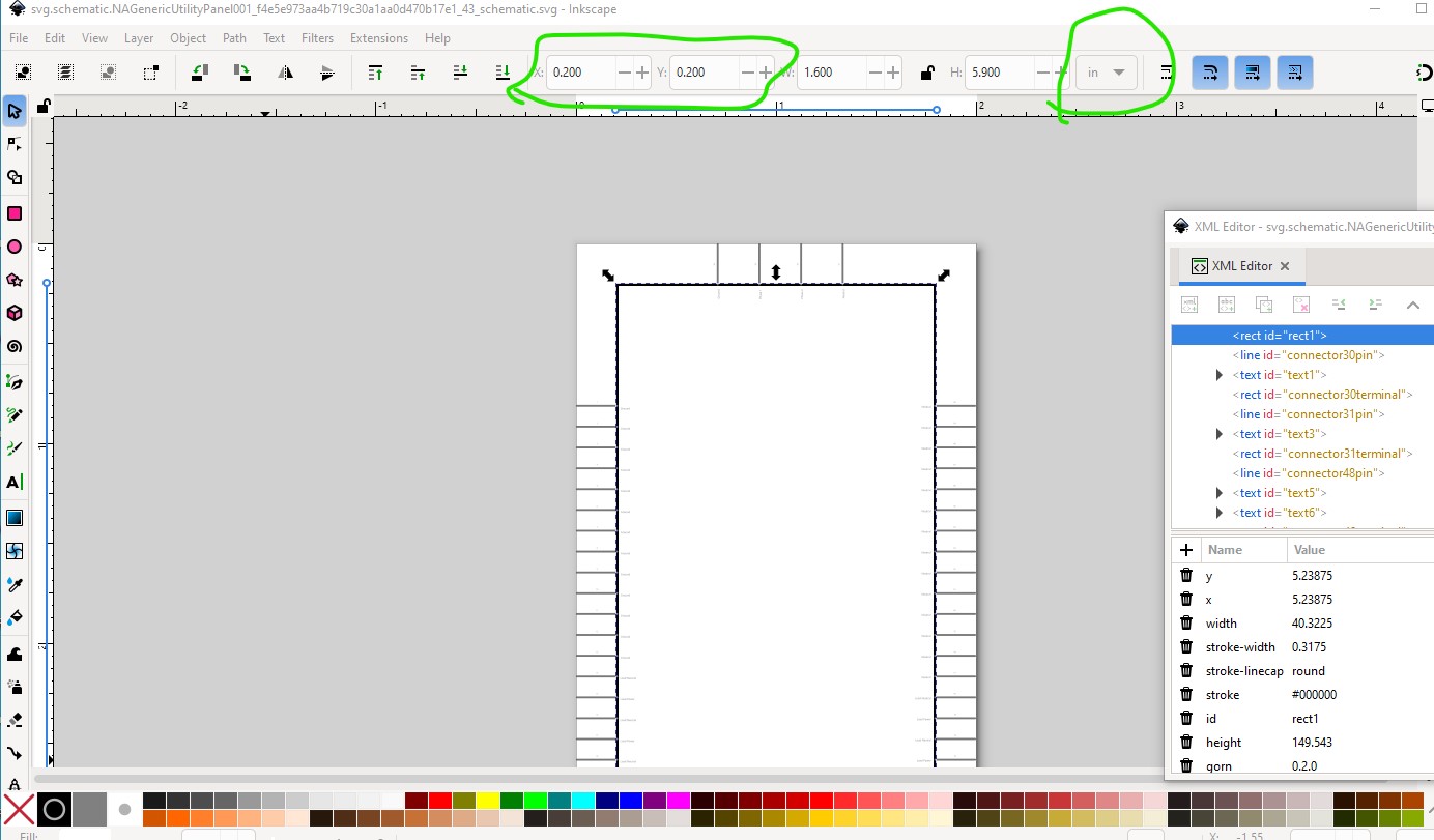
but the pins are incorrect as they are not on 01.in boundaries

As noted I would use Randy’s Inkscape extension to make a new schematic, but you can manually adjust all the pins although it is a lot of work with so many pins. So on to correcting the font size. Here is a correctly scaled schematic with the first pin replaced with your text (to make it the same size in both svgs)

the font size is set to 49px as specified in the part file format document, but because of the scale change the height and width measurements of the text are what is of interest here. This is the current (too small value of the font size. To correct it I increased the font size by trial and error to get the dimensions close to what the correct svg is.

that produces this correctly sized text (and the font size can then be copied to the other text via xml editor in Inkscape!)

I also changed the fill to the correct #555555 color. Pcb is currently broken due to some pins (circled in red here) not being defined in the svg file. That causes the red circle where those pins are placed in the middle of the part.

Your best bet would be to suppress pcb view. Instructions on how to do that can be found in this tutorial (although it requires editing the fzp file to achieve, parts editor can’t make this change AFAIK.)
Hope this helps, if you have questions feel free to ask. Always happy to help people make good parts.
Peter