Hi,
I am totally new to making parts in fritzing.
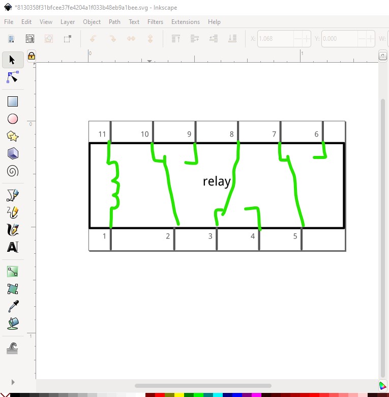
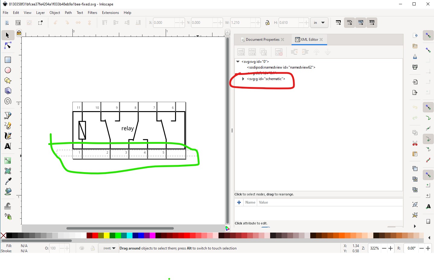
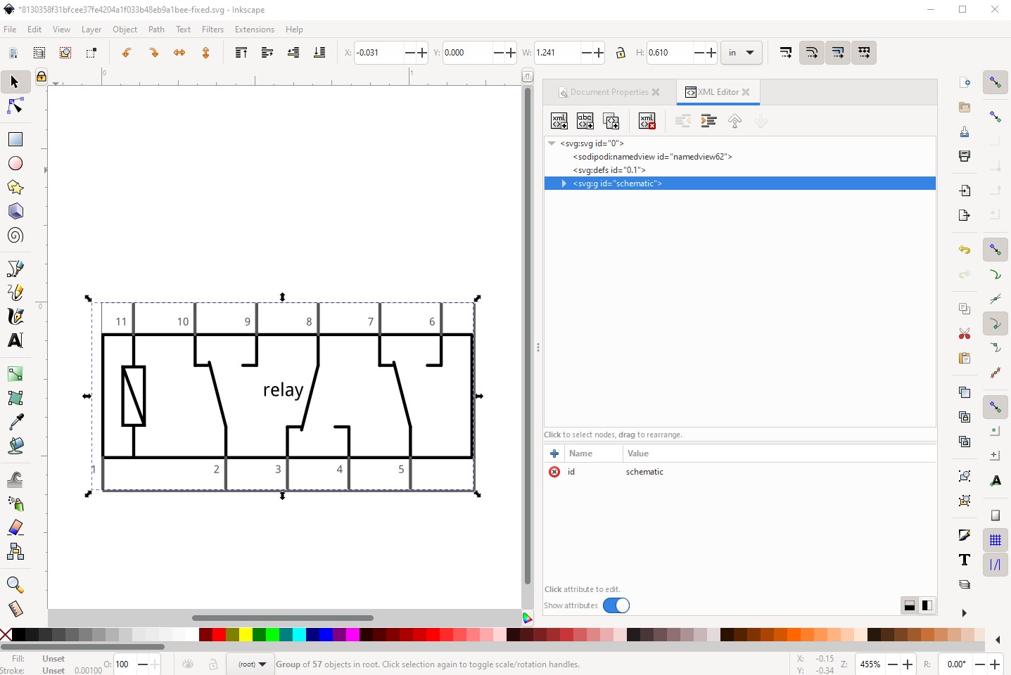
I have made a picture of the schematic part I want to use in inkscape and saved it as an svg.
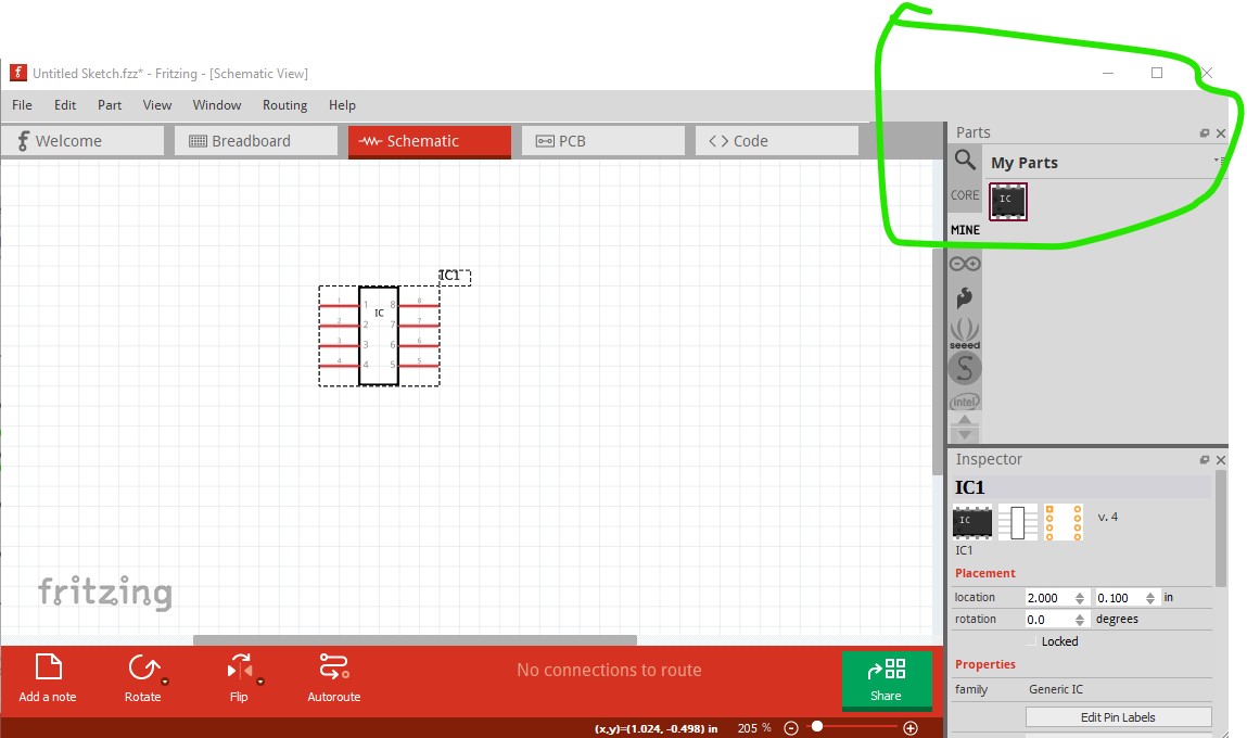
I opened the parts editor in fritzing and loaded the image.
The part shows up almost correctly but there looks to be something else behind it that is insisting on putting dotted and blue coloured boxes on the drawing wherever I have the mouse?

I would now like to make each connection available to be used in fritzing, can I/ do I make these in the editor and how do I localise on each pin so the picture recognises it as a pin.
I am assuming that I am far from doing what I want to do.
Can you help?
thanks,
Bob.
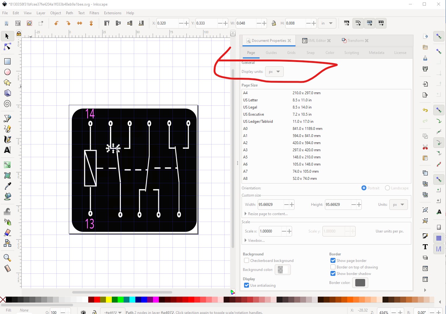
added… the edit page makes it look as if I have uploaded the file but I can’t see any other way of uploading it? Try this the svg
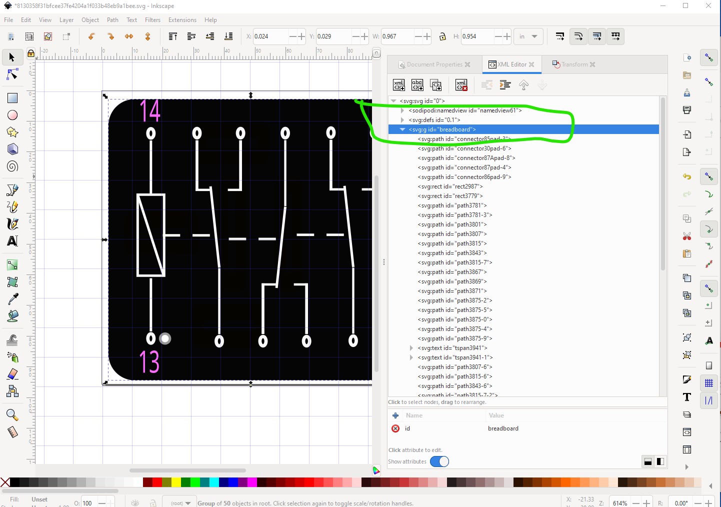
The upload worked fine. The forum renders the uploaded svg, and if you right click on the image and select save image as it will download the svg. That said the svg format is incorrect for breadboard and has a number of extra (and likely unwanted!) connectors. The layout is more usual for the schematic svg, breadboard is usually an image of the part with the connectors specified. The svg is set to be an incorrectly formatted pcb svg though (it has copper layers which are not used in breadboard) and is dimensioned in px which usually causes scaling issues.
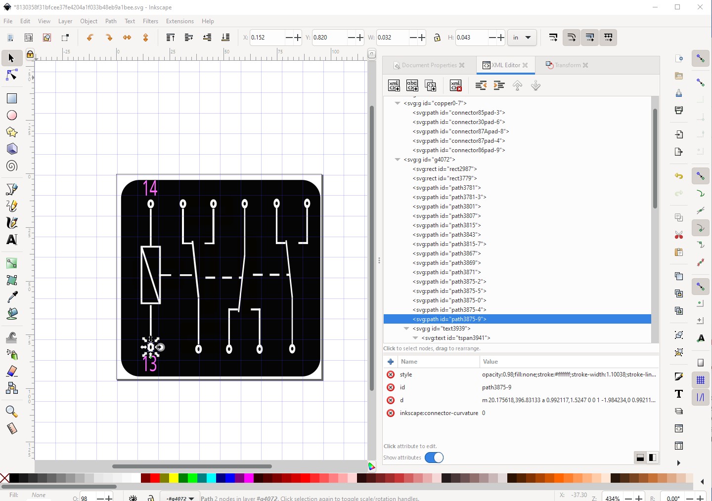
The units wants to be in inches or mm not px. Fritzing will guess which of 72DPI or 90DPI is in use and sometimes get it wrong. In addition current Inkscape is using 96DPI which will make the scale almost certainly wrong. For breadboard you likely want the connectors to start at connector0pin and go up in sequence starting at the bottom left pad:
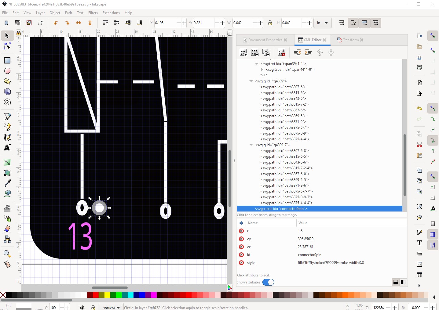
it should preferably be a circle rather than a path (although either will actually work) like this:
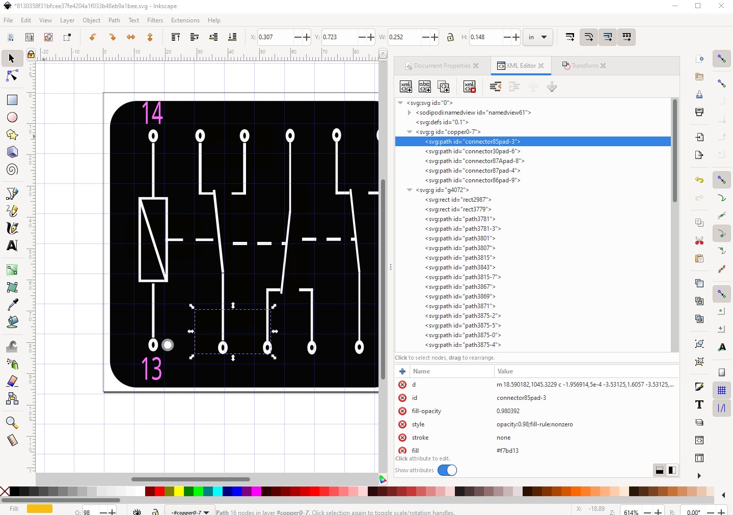
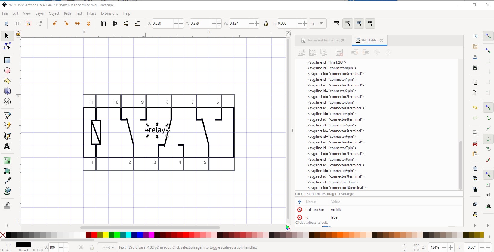
parts editor is likely reacting to the various (incorrect) connector definitions like this one:
which is likely the cause of your unexpected images. The breadboard svg should have a layerId of breadboard like this:
These two sets of tutorials apply to current versions of Fritzing and may also help (I tend to not use parts editor but rather edit the underlying files, the video tutorials do tend to use parts editor though)
Peter
Thank you peter.
I guess that has taken quite a while to produce.
I have been making changes and just editing the file with them.
I will work through your answer tomorrow as it is now after midnight but would you mind just looking at the link I have produced, I think, and getting the file from there to see if it has the same problems, I have altered it in inkscape quite a few times since I put the original question up and the link is the new version.
Thanks,
Bob.
I have even altered my first post to say it is a drawing of the schematic and not the breadboard.
Ah! For a schematic the svg is also incorrect. For schematics the best starting point is this Inkscape extension as it will create a correctly formatted svg that you can change:
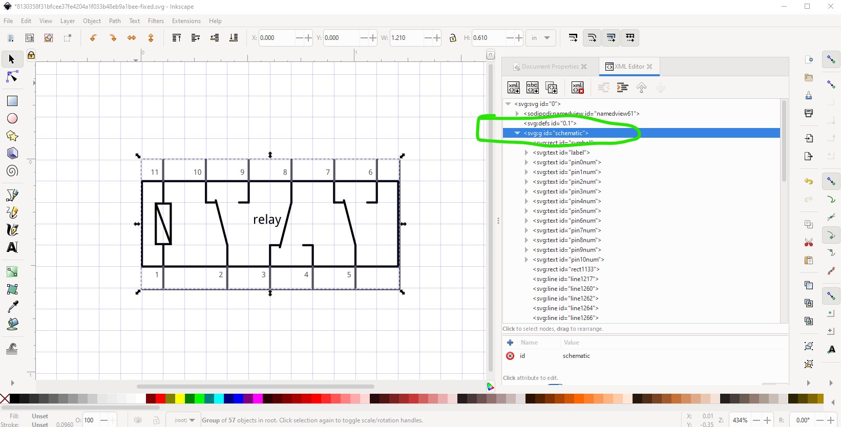
at the correct scale with dimensions in inches. In this case you will need to change the default (which is a box with pins) to have the correct layout of the relay pins but if you start from that svg you will have the correct layout of the svg. You should ungroup the svg before making changes, modify it to what you want, then do an Edit-> select all then Object>group and name the resulting group to “schematic” to have the correct layerId.
edit:
Here is a schematic svg made with the Inkscape schematic extension. Started from your original svg
then deleted everything

and started the fritzing->fritzing-schematic extension in Inkscape
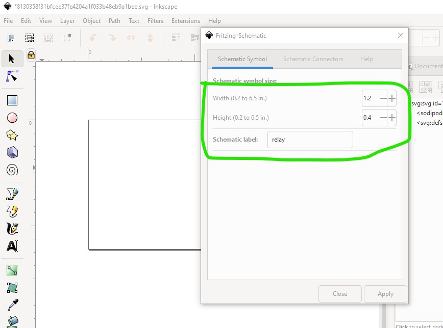
here I cheated (I had to redo this after making it too narrow the first time!) to get the correct length and width parameters. Since I don’t know the part number of your relay I just used relay.
Then I specified 5pins on the bottom and 6 pins on the top.
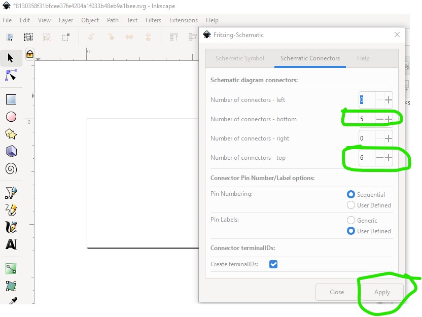
then hit apply which brings up the pin number windows
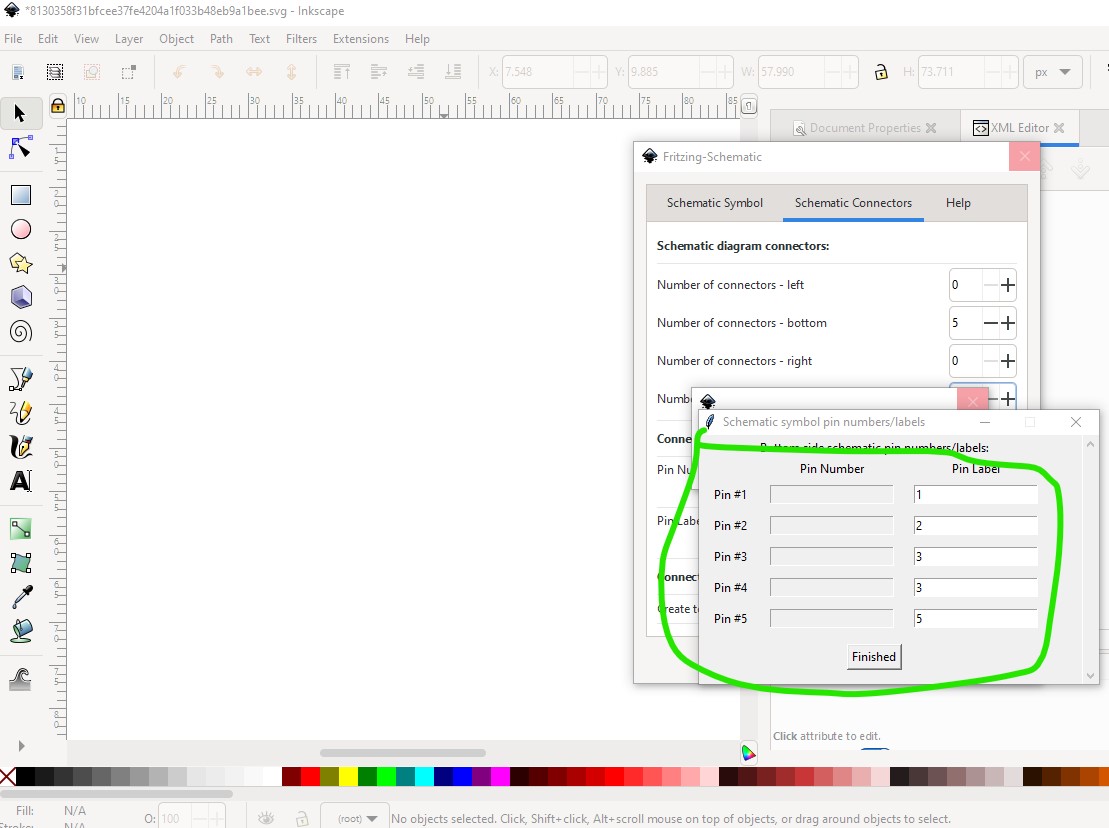
here I just used the pin numbers as we will delete them later.
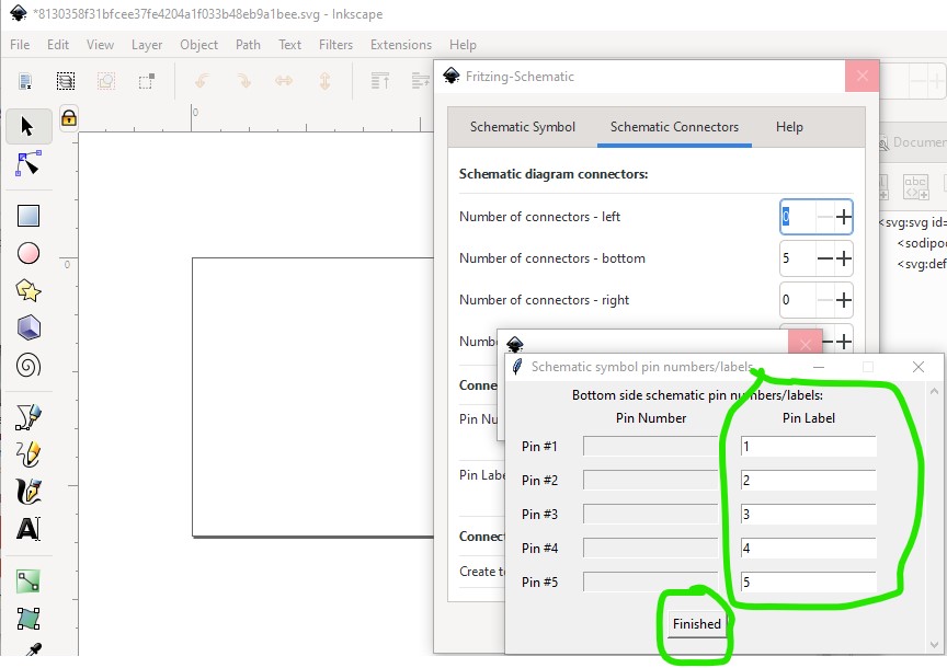
Then hit finished and do the same for the top connectors:

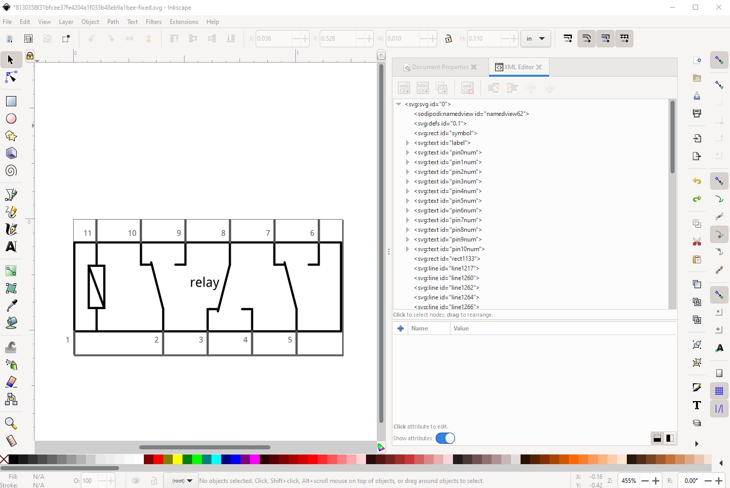
then hit finished and the extension creates the svg in the correct scale, format and colors to meet the graphics standards and looks like this (which needs some editing in this case!)

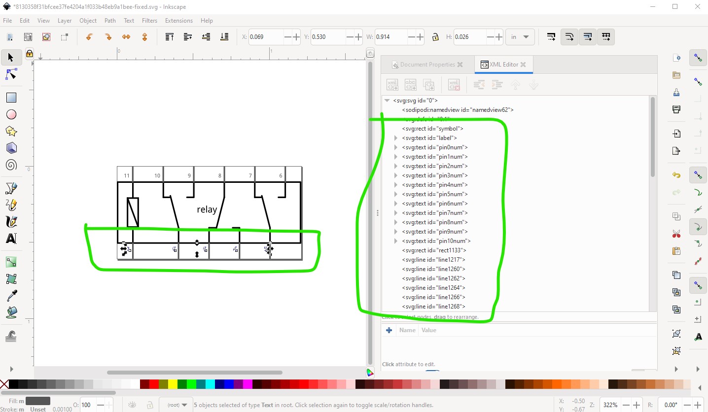
first select group schematic in xml editor and either hit cntrl-G or Object->ungroup to ungroup the svg to make changes.
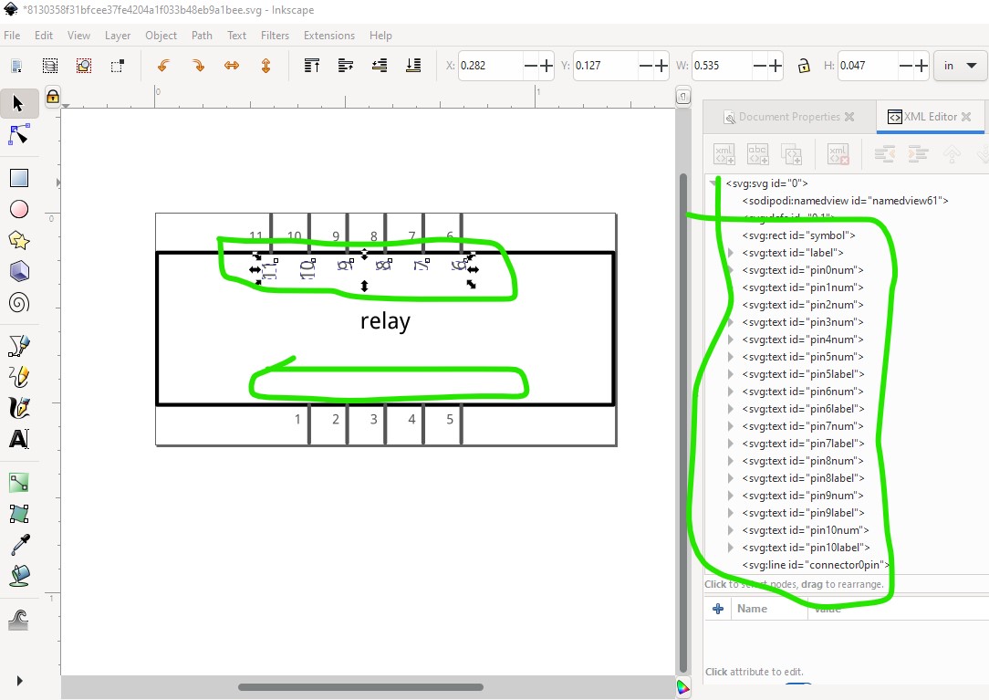
first delete all the pin names we added as we don’t want them in this case. Select the entire first pin with a select box (to get both connector0pin and connector0terminal) and use the tool bar x decrement button to move the pin to the left edge of the rectangle (because the tool bar is set to inches, this will maintain the correct 0.1in spacing!)
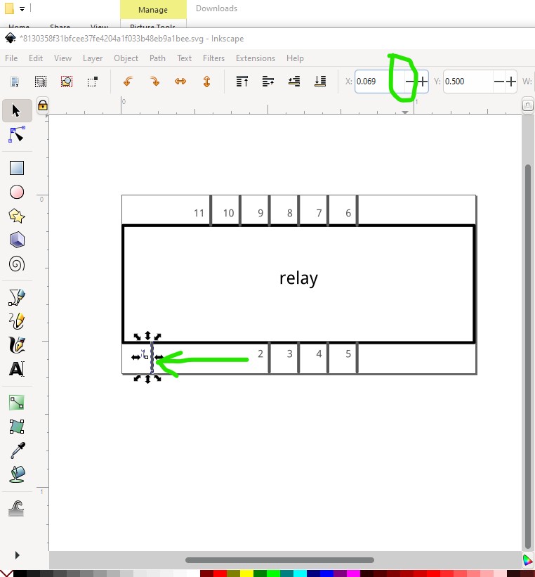
now do the same to all the rest of the pins to make it look like this (we will add the green lines in a bit!)
now add the lines to duplicate the original svg like this
then do an Edit–>select all, Edit->resize page to selection and Object->group to set the layerId. Rename the resulting group “schematic” so set the correct layerId then File->Save as and select save as plain svg then save the svg.
That creates this svg which should load correctly in parts editor. You may need to adjust the pin designations in the fzp file as this svg starts at connector0pin as pin 1 up to connector10pin for the last pin on the top left which may not match your part. You will likely also want to change the label relay to something more appropriate. Below is the above svg:

Peter
Crikey, that’s a lot of work you have done for me. I do appreciate it.
I downloaded the inkscape extension, would you like to inform Randy that it is done via the edit menu – preferences – system not edit menu - user preferences - system?
Just a small thing but he does give you a mention for the testing you did.
I ran through the instructions as you laid them out. Everything went fine til I got to capture 7 (remove the pin labels) for some reason my version fails to delete the copy already on the screen and replace it with the new version? I finished up with layers of the same thing, as they were directly on top of each other I didn’t notice they were in layers but when I removed the labels the picture showed the labels still showing ‘pin1’ with the number 1 ‘under’ the letter P. It was only when I selected the whole thing and moved it accidentally to one side that I noticed there was an almost identical copy underneath it. After I moved and deleted all the copies I didn’t want did I get to your capture8?
I deleted all the pin names. For some reason it doesn’t allow me to use a select box? Even after I highlighted and did object – ungroup?
I had to click on the item in the XML editor to highlight a number or pin but then they moved as you said.
I used the draw Bezier icon and got straight lines for the next stage but it took a steady hand.
I couldn’t see anywhere to rename the resulting group so I downloaded your svg.
It looks like I can only open the parts editor in Fritzing by highlighting an object and then opening the editor for that object? If I then load image to view and enter the relay it has another item as its breadboard item? I couldn’t see any other way to do it so that is what I did? I finished up with the relay in the parts editor but the font had failed to load properly?
Can you see what I am doing wrong?
Bob.
I am fairly sure my error is having to open the XML editor with a component selected but I can’t see any other way?
This is normal behavior. If you run the extension twice it will write a second copy of the schematic on top of the first (it will have a new group name so you can then delete the old one all at once if you like.) That is why I deleted the original svg before I started, you need to start the extension on a blank canvass.
I would guess that the text was within a group. Select boxes won’t work on a group, so I usually start by doing an Edit->select all then Object->group then do multiple ungroups (usually via the keyboard) to remove all groups. Then select should work. Here the group schematic still exists so the select on the text doesn’t take when you exit the select box:
Doing a shift-cntrl-g to ungroup schematic makes the select on the text box work:
Now the delete key will delete the selected text which it wouldn’t before.
Again that is likely because it is in a group and thus won’t select with a select box. Here the group schematic still exists, and I can select the connector by clicking on the pin in xml editor and it will move, but the terminal just under it will not and in this case both the connector0pin and the connector0terminal need to move to be correct, so you need to ungroup so select will work like this. Here with the svg ungrouped, this selection will move both connector0pin and connector0terminal when the tool bar is incremented or decremented and thus keep the correct alignment.
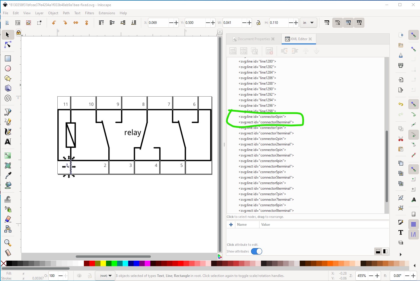
Here both connector0pin
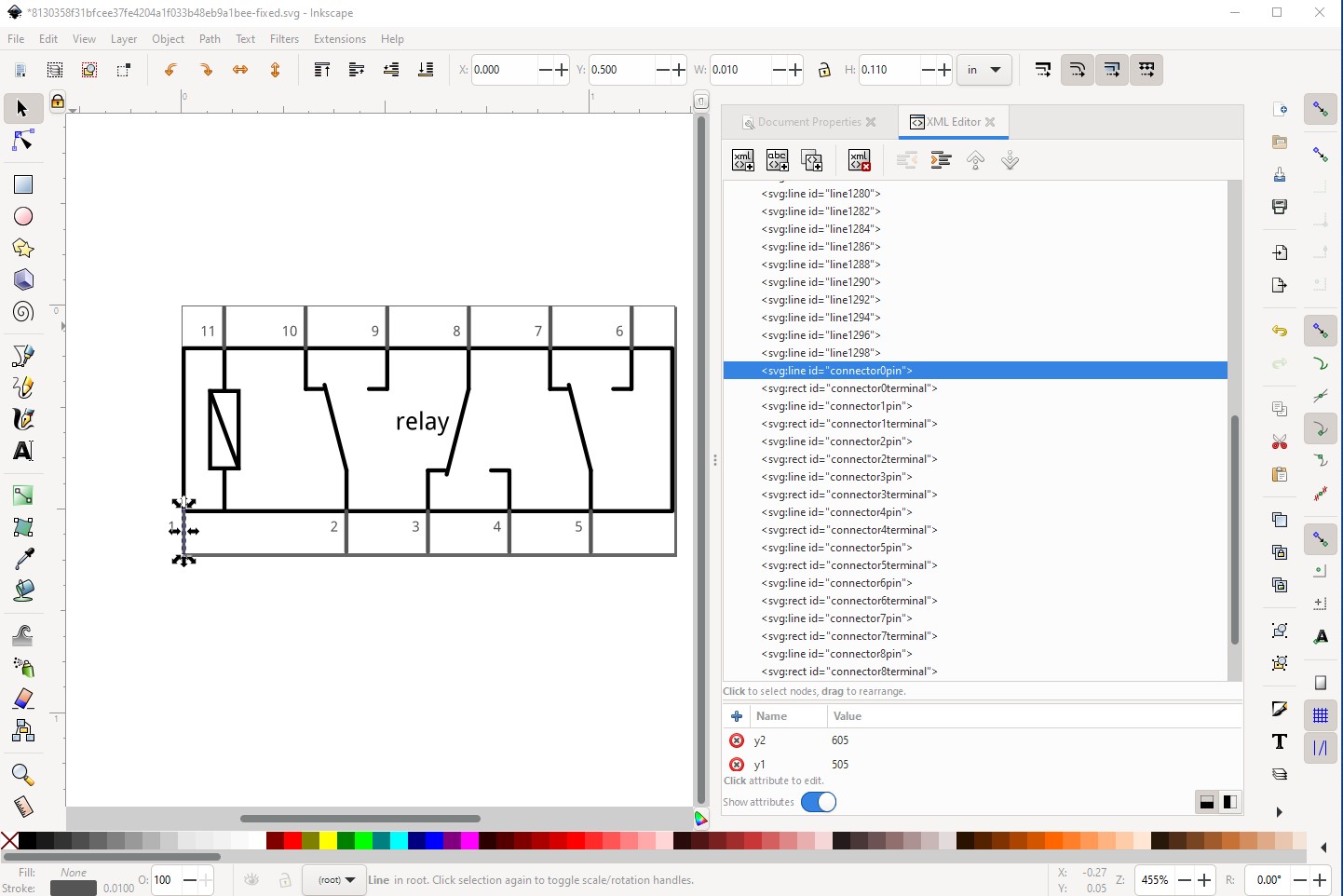
and connector0terminal (a rectangle on the bottom of connector0pin) have moved together as they should.
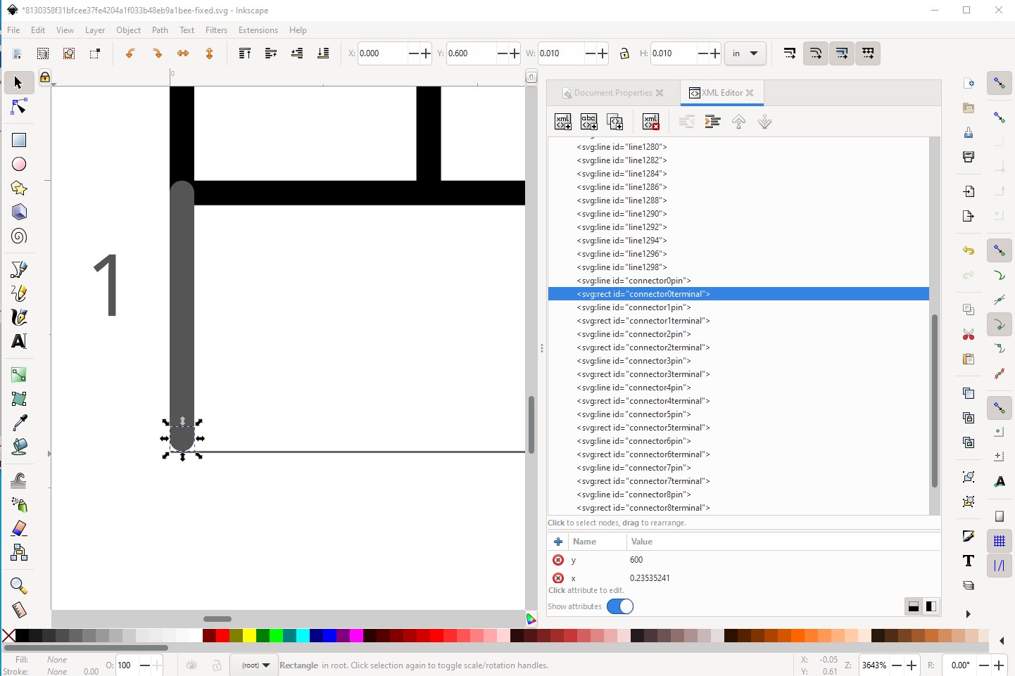
without this the terminal won’t have moved and the wire in schematic will connect to the wrong pin (it connects to connector0terminal!)
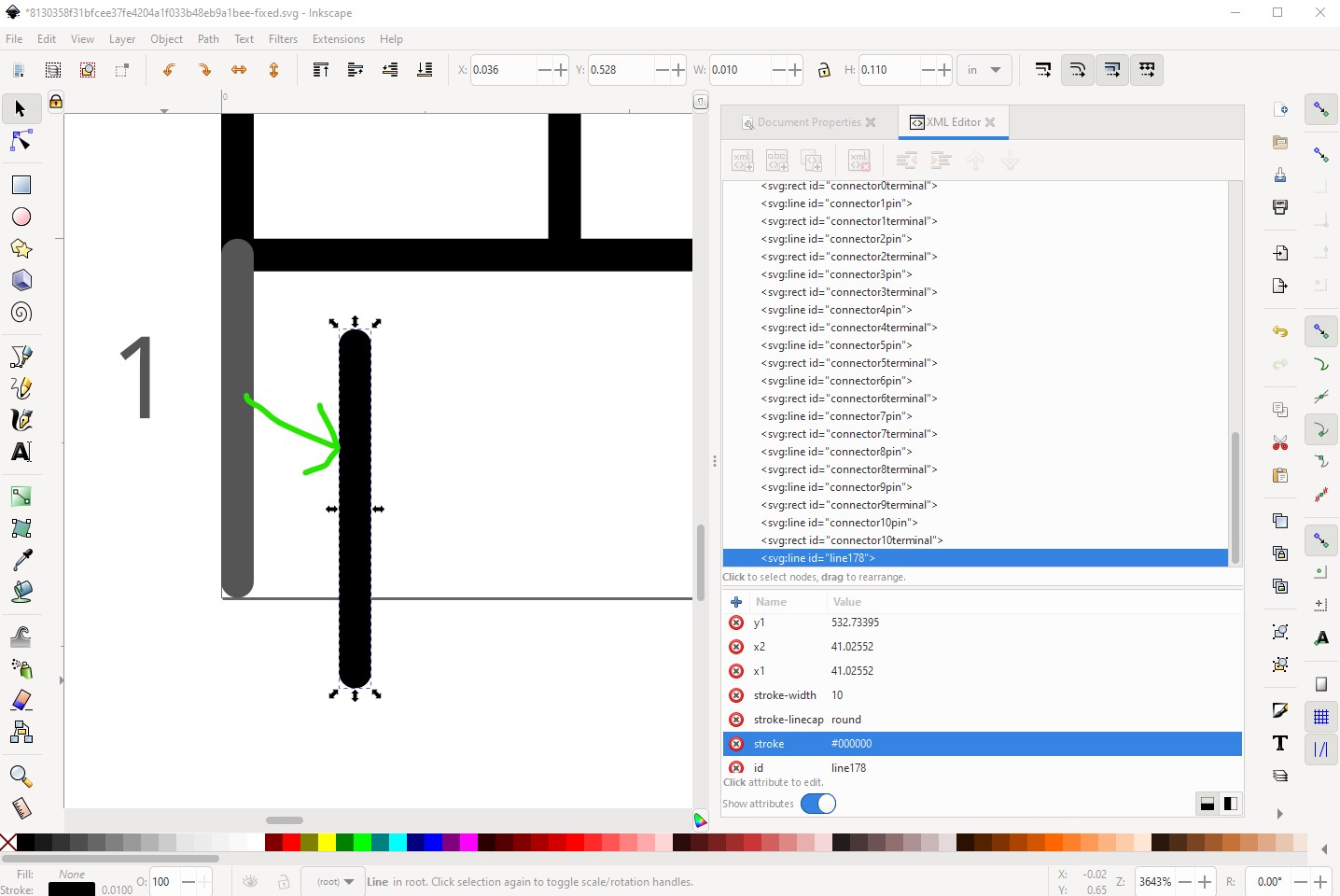
I cheated ![]() Inkscape understands but won’t create lines (lines are an Illustrator construct.) To make my interior lines I duplicated a pin like this:
Inkscape understands but won’t create lines (lines are an Illustrator construct.) To make my interior lines I duplicated a pin like this:

Then changed its color to black in xml editor and dragged it where I wanted it, then used the scale handles (or the height and width in the tool bar) to set its length.
I find this much easier than trying to draw a line in Inkscape! For the group starting from the ungrouped svg
Do Edit->select all then Object->group
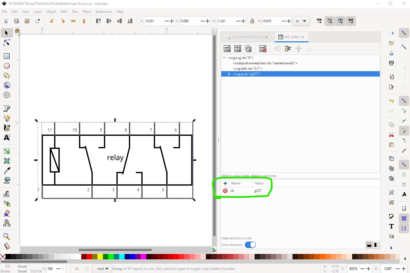
then change the group (g237 in this case) to schematic using the xml editor
You need to highlight a fritzing part and then invoke the parts editor. You can do that in either a sketch or in the parts bins. The current fzp and svg files for the part will then be loaded in to the parts editor. You can replace any of the views svg by selecting that view and clicking File->Load image for view. That will replace the current svg with the one you select (which needs to be the correct format for the view!)
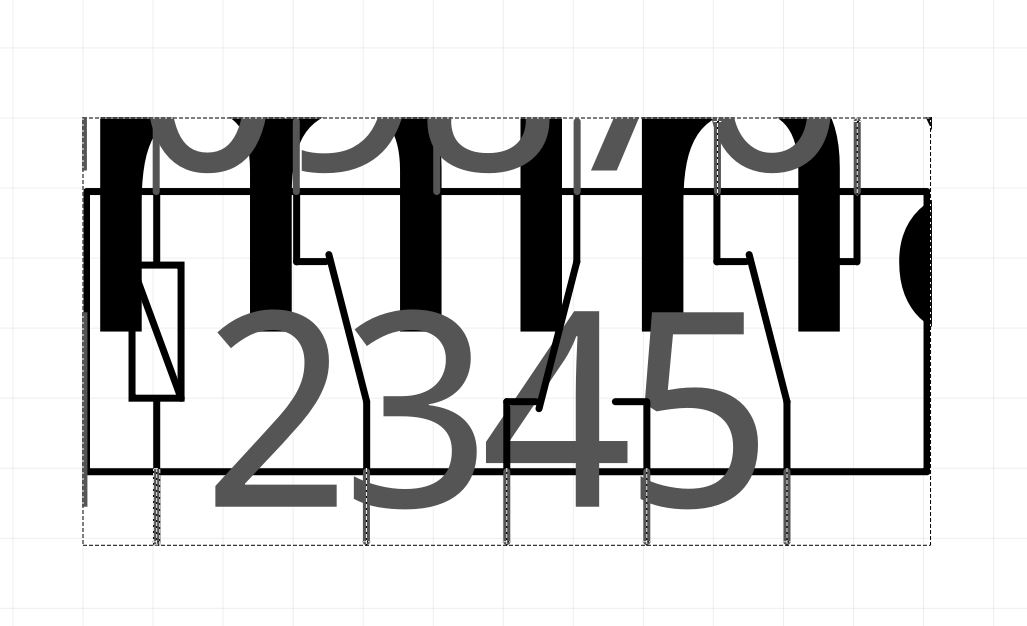
Ah! This is a Fritzing quirk, the font sizes in the svg can not have px appended to them. CSS requires font-size to have a px appended so Inkscape appends them. I usually fix this by running the part of svg through FritizngCheckPart.py which among other things removes the px from font-sizes. The alternative is to edit the svg with a text editor and do a global replace of px with “” to convert this:
<text
   x="591.27441"
   y="305"
   font-family="'Droid Sans'"
   font-size="60px"
   fill="#000000"
   id="label"
   text-anchor="middle">relay</text>
<text
in to this
<text
   x="591.27441"
   y="305"
   font-family="'Droid Sans'"
   font-size="60"
   fill="#000000"
   id="label"
   text-anchor="middle">relay</text>
<text
where font-size=“60px” has changed to font-size=“60” to keep Fritzing happy. As you see there are many rules and gotchas in parts making! Inkscape is mainly for graphic artists, Fritzing use of it is non standard and takes some post processing. Hope this helps!
Peter
Hi Peter,
I downloaded your schematic again and using the notepad I replaced all the 'px’s with space. When I loaded image for view into the editor it looked fine.
I only managed to connect a wire to connectors 1 and 2. I noticed in the parts editor that there were only 2 pins in the connector list in the top right corner.
I clicked on the tab for connectors and altered the number to 12. going back to the schematic view showed there were now 12 pins numbered 0 to 11 and all ticked.
If I hover my mouse over the relay it goes blue?
If I hover over each of the pins I get a small circle appear at the ends where the wires would connect. clicking on the file tab says save or save as new part, it doesn’t say where it saves?
I am assuming it is saving somewhere that is not updating the item in the schematic drawing of fritzing because I can still only connect to pins 1 and 2?
I don’t know what I have done now.
I decided to start again downloading your final schematic, I altered the ‘px’ and loaded the image for view in the editor over a 4 pole that I managed to make a breadboard diagram of a few years ago, I think you helped me there?
The schematic in the editor showed the relay fine but now if I hover over the centre of it I get a blue relay centre, if I hover over the top or the bottom it all goes blue? Do I still not have it grouped properly?
I changed the 2 connectors to 12 again and get a small ring highlighted if I hover over the end of each pin.
I saved and went back to the fritzing view, dragged the relay schematic I had just pulled into the editor and got a good representation of the relay but now it is bright red and purple if I hover over it? There is a small spot in the middle and all the wires lock from the centre of each ‘pin’ (as opposed to the end) to the small spot in the middle no matter where I try to place them.
I am goin g to keep trying to solve this but would welcome any help.
Bob.
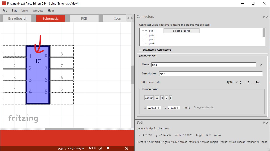
While I rarely use parts editor (because of problems just like this!), I think that after resetting the number of connectors to 12, you then need to then click on each connector in turn and click the Select Graphic button to set the connector (usually I can’t make this work in Parts editor, so I edit the files directly!) Then you need to set the terminal point (W for west in this case) to set where the termnalId will be on the left end of the pin in this case.
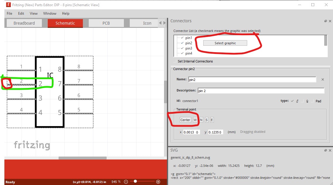
If I hover on the square (at the red arrow) in Parts Editor I get a blue square, but I don’t know what it signifies since I don’t think you can edit anything in the blue box (although I may be wrong!)
It will save the part in to the mine parts bin. Here it is currently empty.
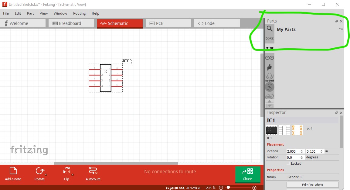
When I click save as a new part and then ok to the prefix, it saves the part in the mine parts bin like this:
If you right click on the part in the mine parts bin and select Export part, it will write the part to a .fzpz file in the file system (it will prompt for a file name and location.) If you then upload the resulting .fzpz file (upload is 7th icon from the left in the reply menu) I can tell you what is going wrong by looking at the files and maybe figure out how to make it work in parts editor.

Peter
I can’t seem to get it to work on parts editor either no matter what I do.
I now have pins 1 and 3 to 12 (11 and 12 don’t have ticks against them) nothing I do seems to change this? If I click on
pin 1 I get nothing,
pin3 the small circle at the end of pin3 highlights,
pin4 the small circle at the end of pin 5 highlights,
pin5 small circle end of pin 6,
pin6 small circle end of pin 7,
pin7 whole of pin 8 highlights,
pin8 whole of pin 9 highlights,
pin9 whole of pin 10 highlights,
pin10 whole of pin11,
pins 11 and 12 don’t have ticks alongside them and nothing happens if I click on them. Nothing I do seems to change this.
I don’t have the next box down the right side that you have, the ‘connector pin2’ box? I just have SVG and layers?
I have been trying fruitlessly to get this to work.
If I drag another component onto the screen and try to connect wires to the relay it will lock onto the middle of pin1, not the end (I assume this is corrected in the box I don’t have above?) pins 2 to 5 just spring into the centre of the relay where the ‘a’ of relay is, pin6 goes to the correct end, pin 7 to the centre of the pin and pins 8,9,10 and 11 to the centre of the item. I am not even sure I have changed anything from the file you sent me so I have included the one I am working on here.
relay.fzpz (5.6 KB)
Is there any way of stopping it from being pink on the screen and blue when I hover my mouse over it?
Would you mind seeing if you can solve the problem of the pins not connecting to the ends for me?
I have managed to add it to one of my breadboard attempts from long ago
It almost meets my needs, it is very similar to the appearance of the relay I am trying to make the schematic of.
see https://uk.rs-online.com/web/p/relay-sockets/1217802.
Thanks,
Bob
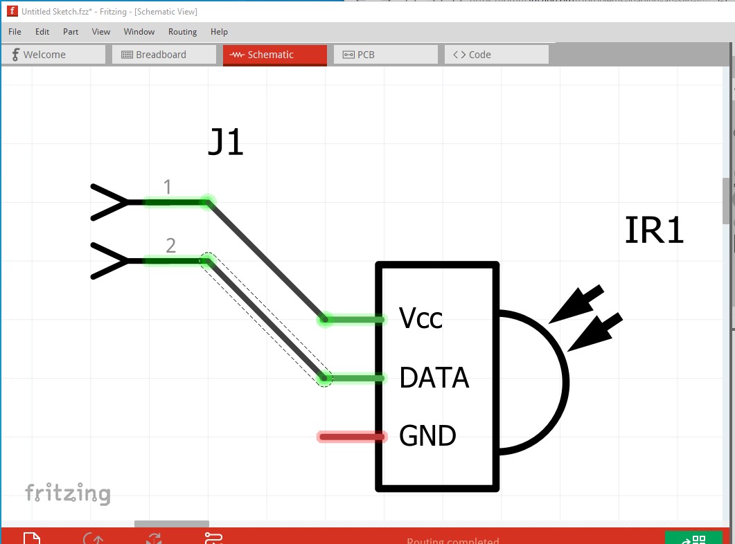
The .fzpz appears to be an IR sensor which is I don’t think what you meant:
and is working correctly in schematic:
That said here is a part that you can modify to do what you want. I started with my original schematic and added a basic breadboard (11 pins and a square) and pcb (again 11 pins in a square.) If you unzip this fzpz file you will get the relevant svg files and can edit them to change them as you want. You either need to run the part.relay_1.fzp file through FritzingCheckPart.py to remove stray px in font sizes or edit each svg with a text editor and globally replace “px” with “” to avoid font size problems. This should work as is if imported to parts editor as all the correct formats are present, the pins should appear correctly selected as is.
relay.fzpz (4.3 KB)
Peter
Peter, that is brilliant thank you.
I am hoping you won’t get the impression I am just asking you to solve the problem for me. The file you sent me is almost exactly what I want.
I am trying to solve it myself but have come up with a few problems.
I would like to alter the pin numbers for a start, I assume you make the item in inkscape?
I assume the schematic is just a case of ungrouping in inkscape, moving the pin numbers, regrouping and replacing the schematic file to get the numbers correct with the base I have? I haven’t tried that yet.
I am working through inkscape and altering the position of the pins in the breadboard file to fit my needs, I have also decided to try to make a similar breadboard base for the 4 pole I use instead of the one I added in my last thread, your version looks better.
To this end I have moved the pins around (I managed to move one pin and then port it back to fritzing to see if it worked, I used notepad to alter the partrelay file (and renamed it slightly to partrelay_2.fzp) to accept the new file and it worked, eventually, so now I am trying to alter all the pins and add 3 more.
If I copy and paste them they show on the screen and I can move them to the position I want but the names in the XML editor show as
svgrect id=“connector5pin-4” (I copied pin 5)
(or -2 or -5) can I change them to
svgrect id=“connector11pin”
(or 12 or 13)? I can’t see anywhere that allows me to change them.
EDIT:- I am going to leave that last bit to show I am trying to solve it. I found out how to rename them, in the box to the right of the xml editor the bottom line is the id name 
I am grateful for your help. It has allowed me to progress. I am going to spend a few days trying to solve the other problems so I may get back to you.
Am I right in saying the svgrect id in inkscape is the item that allows you to ‘hook’ a wire to it in fritzing?
The connector0pin (or connector0terminal) id in the svg is what Fritzing is looking for to connect the wire to.
Peter
More completely, Fritzing is looking in the svg for an id to match whatever the fzp shows as the id for the connection and view. Which is normally connector«number»pin and/or connector«number»terminal. It could be something else, like connector«number»pad for SMD devices on PCB view.
That id could be on various svg elements. rect, line, circle most common. It does not work on a group “g”, and path can be tricky to get right.
Hi Peter,
I thought I would just update you on my progress.
I am quite pleased with my little self. I still have your 3 pole version but I have managed to convert it to a 4 pole and used pictures for the breadboard views see
relay1.fzpz (173.1 KB)
relay2.fzpz (1.2 MB)
relay3.fzpz (1.7 MB)
I just used a number for the icons but the schematic is the same in each case.
I moved the terminals around in inkscape and then altered the part.relay.fzp to suit.
Thanks to your start I have managed to understand and manipulate most of it.
I don’t quite understand why the inkscape XML editor shows so many embedded svg layers and I tried to move some of them around without much success, in fact if you keep zooming in to relay3 in the fritzing breadboard view eventually the original relay picture shows but disappears again when you zoom out? I think this has to do with the svg layers in the code but I can’t see which?
I assume these could be useful to anyone else using these relays, is there somewhere I can donate them for anyone’s use when I have finished making all of them?
Bob.
There are some problems. In relay1.fzpz the breadboard file is incorrectly named and thus it doesn’t load:
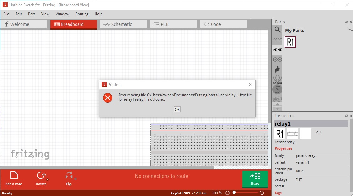
This is because the fzp file looks like this:
 <views>
    <iconView>
      <layers image="icon/omronrelay1icon.svg">
        <layer layerId="icon"/>
      </layers>
    </iconView>
    <breadboardView>
      <layers image="breadboard/relay_1_breadboard.svg">
        <layer layerId="breadboard"/>
      </layers>
    </breadboardView>
    <schematicView>
      <layers image="schematic/relay_3_schematic.svg">
        <layer layerId="schematic"/>
      </layers>
    </schematicView>
    <pcbView>
      <layers image="pcb/relay_1_pcb.svg">
        <layer layerId="silkscreen"/>
        <layer layerId="copper0"/>
        <layer layerId="copper1"/>
      </layers>
    </pcbView>
  </views>
but the file system looks like this:
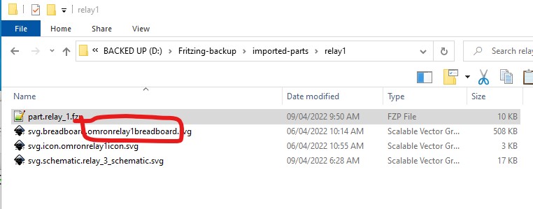
the breadboard svg file needs to match (in both text and case!) the file specified in the fzp file so the breadboard entry in the fzp file needs to change from
<layers image="breadboard/relay_1_breadboard.svg">
to
<layers image="breadboard/omronrelay1breadboard.svg">
to match the
omronrelay1breadboard
part of
svg.breadboard.omronrelay1breadboard.svg
the leading svg.breadboard and trailing .svg tell the loader that this is a breadboard svg and are the same for all svgs. As well the pcb svg file is completely missing so pcb view doesn’t work. In the breadboard svg, there isn’t a layerId so the part won’t export as an image.

Here one of the groups circled in red needs to be renamed “breadboard” to match the line
<layer layerId="breadboard"/>
in the .fzp file. There are also a lot of unneeded groups as you have noticed. Parts Editor likes to add groups to svgs (I don’t know why though) but they can all be removed. To do so select the top group in Inkscape like this:
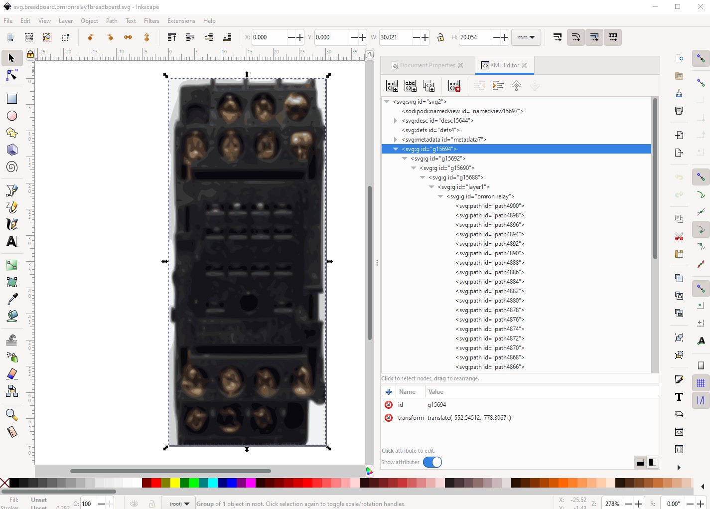
Then on the keyboard hit cntrl-shift-g (or Object->ungroup in the tool bar but I find the keyboard to be more convenient) to remove all the groups like this:
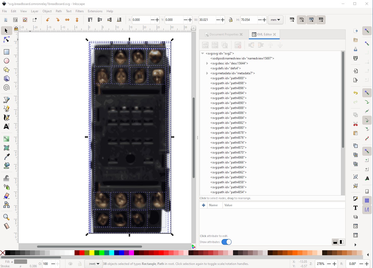
Then click Edit->select all then Object->group to group the entire svg like this
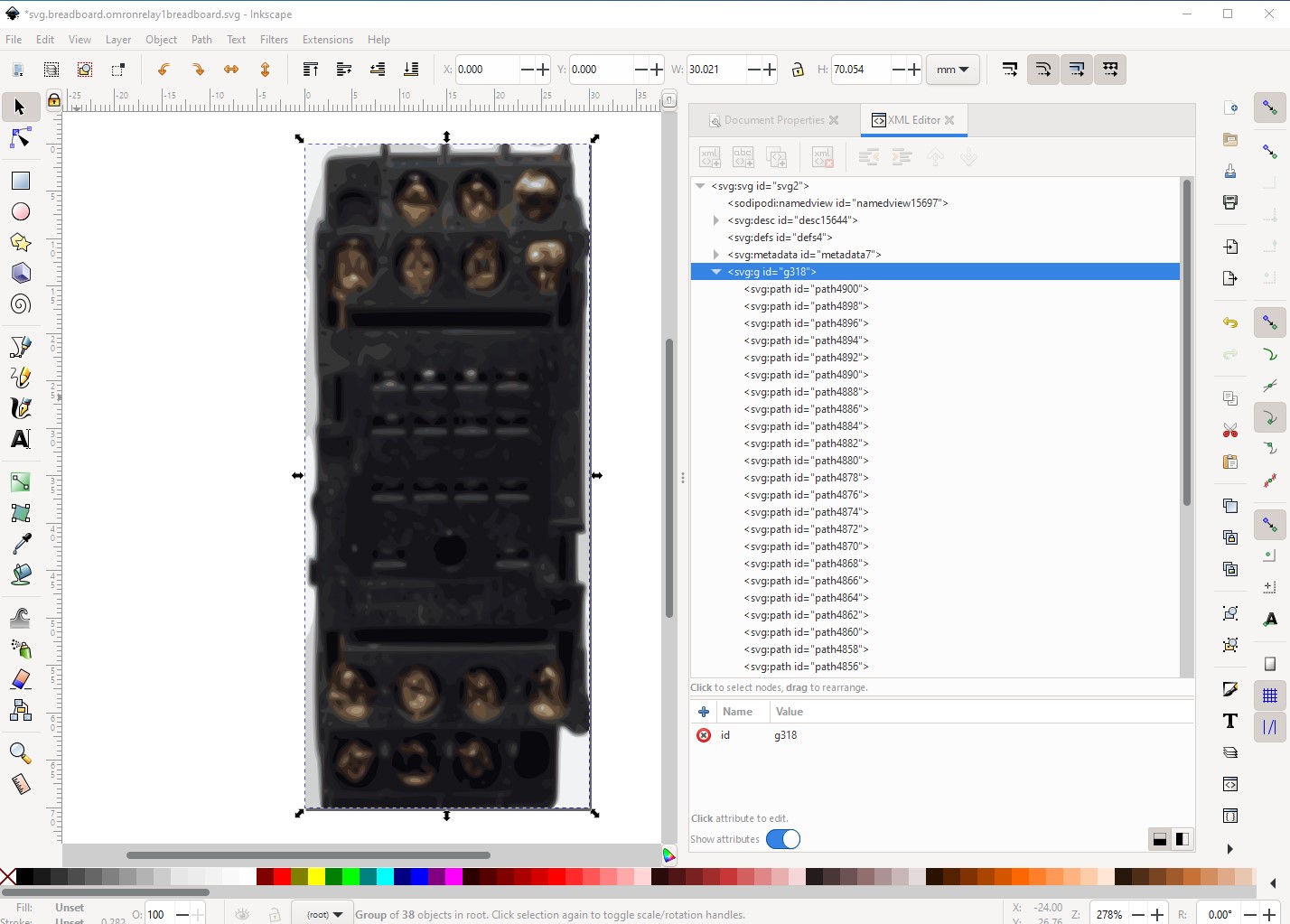
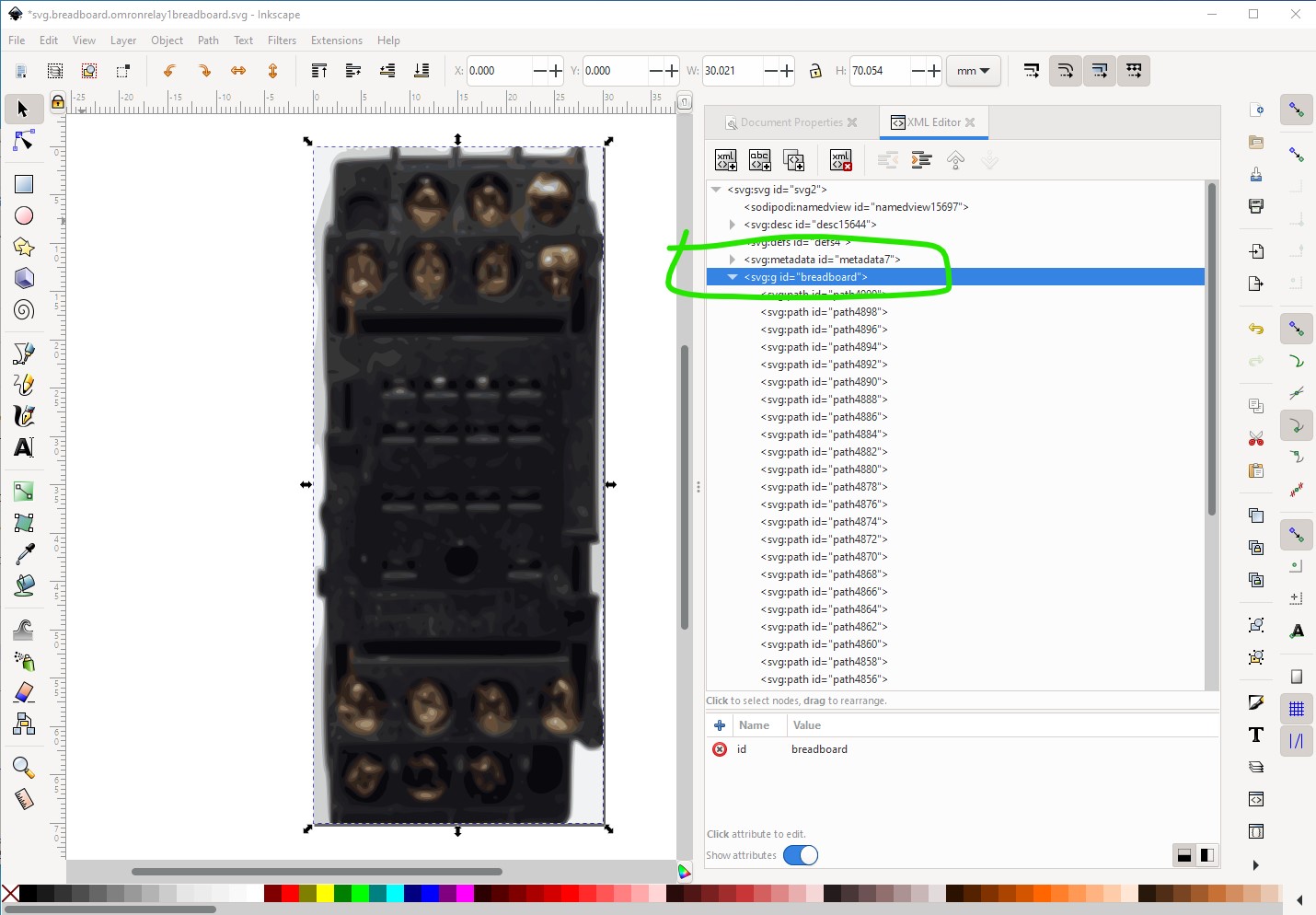
then use xml editor to change group g318 (in this case) to “breadboard” like this
The same thing needs to happen in schematic where the layerId is typically “schematic”, the pcb svg typically needs a silkscreen, copper1 and copper0 group (and in this case you need a pcb svg too!) That said, in breadboard it would be preferable to use drawing elements (paths, rectangles etc.) to replace the image something like this as it looks better:
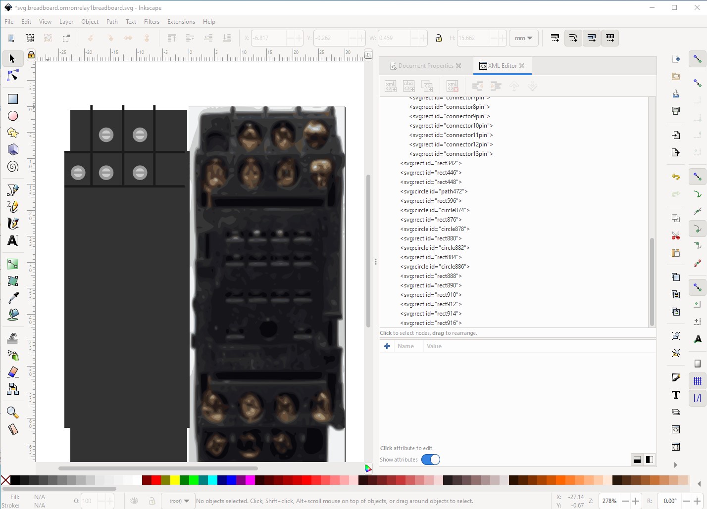
(I only did part of the socket as an example here!) Because it is an svg it will scale when the image is zoomed in or out where the image will get more blurry as it zooms out and less clear as it zooms in (as the image is fixed and won’t scale.) Here is that breadboard svg (with the fzp file corrected so it loads) in Fritzing to show the difference in appearance

and zoomed out

note the new image in the left maintains its appearance because it has been scaled.
Peter
Yes, sorry, I have it correct in the file in fritzing, I must have messed with the files in the zip that I saved, if I export it from the fritzing program it has the alterations you suggest.
I got the impression the leading svg.breadboard. told the loader to put the files in part/svg/breadboard/?
? I have exported the relay from fritzing and it looks ok but I can’t find a layerid in it?
I didn’t add a pcb file as it is not a pcb mounted relay base.
Are you saying that a line such as <svg:g id=“g15688”>
needs to be altered to read <svg:g id=“breadboard” and does it matter which one?
Or as I now reread it I think I remove all the unneeded groups then edit/select all object/group, this creates a new line that I replace the number gXXX with “breadboard” is that correct?
Are you saying to remove all the groups above the list of
svgpath id=“path4900” (in this case and similar under it)
like the ringed below
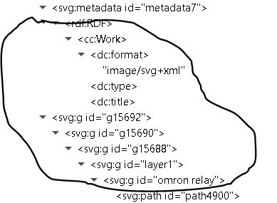
?
Looking at the omronrelay3breadboard.svg file in notepad, this part, including in the ringed part above looks to do something

If I remove them might this remove the breadboard picture that appears if I zoom in?
Bob
That is exactly what it does, but in addition the next part specifies the name of the svg file, and that need to match in name and case with the file in the file system.
Then you need to suppress the pcb view and remove the pcb definitions from the svg file. I believe how to do that is covered in my tutorial.
Yes in a set of nested groups, as long as one of the groups has id breadboard Fritzing will be happy. The layerId doesn’t refer to what Inkscape thinks of as a layer (and I don’t exactly know what a layer in Inkscape is!) but is rather a group with the id of “breadboard” that contains all the drawing elements. The Fritzing documentation refers to this as a layer which is not what Inkscape considers a layer I don’t think.
You need the metadata usually (or at least having it doesn’t hurt anything) but you can and I usually do remove all the groups by ungrouping them and then do an Edit->select all and Object-> group to create a single group that you then need to make the id of “breadboard” to create the layerId.
Peter
OK thank you Peter I will work through that and try to clean it up.
Did you make the new relay picture you show in inkscape it does look neater than the photo I have used.
Bob.