Part-creation-howto-part10-Inkscape-schematic-extension

this is a continuation of

On

https://github.com/revolt-randy/Fritzing-Schematic-an-Inkscape-Extension.

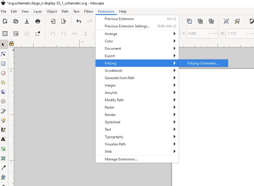
There is an extension for the Inkscape svg editor which will create a schematic svg (which is correctly scaled and configured to meet the Fritizng graphics standards.) I use it pretty much always to make new or usually even existing schematics as it is the easiest way to do so. However I find the current size limits too small (only 64 connectors to a side) so I change the inx file like this to allow larger schematics with more connectors (each connector takes 0.1in, so the maximum size of the drawing limits the number of connectors on a side.)

file (wherever your Inkscape extensions are stored, it varies by operating system!)

Windows (where it is in Appdata\roaming\inkscape\extensions)

inkscape\extensions\fritzing-schematic.inx

or

inkscape/extensions/fritzing-schematic.inx

on the Mac or Linux

change from the default

		<param name="x_size" type="float"   min="0.2"    max="6.5"    _gui-text="Width (0.2 to 6.5 in.)">0.3</param>
		<param name="y_size" type="float"   min="0.2"    max="6.5"    _gui-text="Height (0.2 to 6.5 in.)">0.3</param>

to

		<param name="x_size" type="float"   min="0.2"    max="14"    _gui-text="Width (0.2 to 14 in.)">0.3</param>
		<param name="y_size" type="float"   min="0.2"    max="14"    _gui-text="Height (0.2 to 14 in.)">0.3</param>

to allow more connectors (139 on each side with this setting, for more increase the sizes!)

and from default

	<page name="connectors" _gui-text="Schematic Connectors">
		<label appearance = "header" >Schematic diagram connectors:</label>
		<separator />
		<param name="left_connectors" type="int"   min="0"    max="64"    _gui-text="Number of connectors - left">0</param>
		<param name="bottom_connectors" type="int"   min="0"    max="64"    _gui-text="Number of connectors - bottom">0</param>
		<param name="right_connectors" type="int"   min="0"    max="64"    _gui-text="Number of connectors - right">0</param>
		<param name="top_connectors" type="int"   min="0"    max="64"    _gui-text="Number of connectors - top">0</param>

to

	<page name="connectors" _gui-text="Schematic Connectors">
		<label appearance = "header" >Schematic diagram connectors:</label>
		<separator />
		<param name="left_connectors" type="int"   min="0"    max="139"    _gui-text="Number of connectors - left">0</param>
		<param name="bottom_connectors" type="int"   min="0"    max="139"    _gui-text="Number of connectors - bottom">0</param>
		<param name="right_connectors" type="int"   min="0"    max="139"    _gui-text="Number of connectors - right">0</param>
		<param name="top_connectors" type="int"   min="0"    max="139"    _gui-text="Number of connectors - top">0</param>

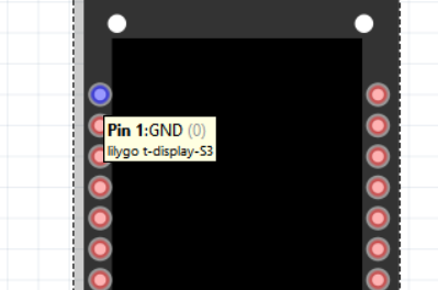
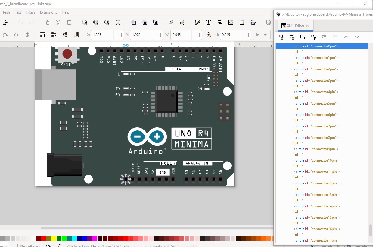
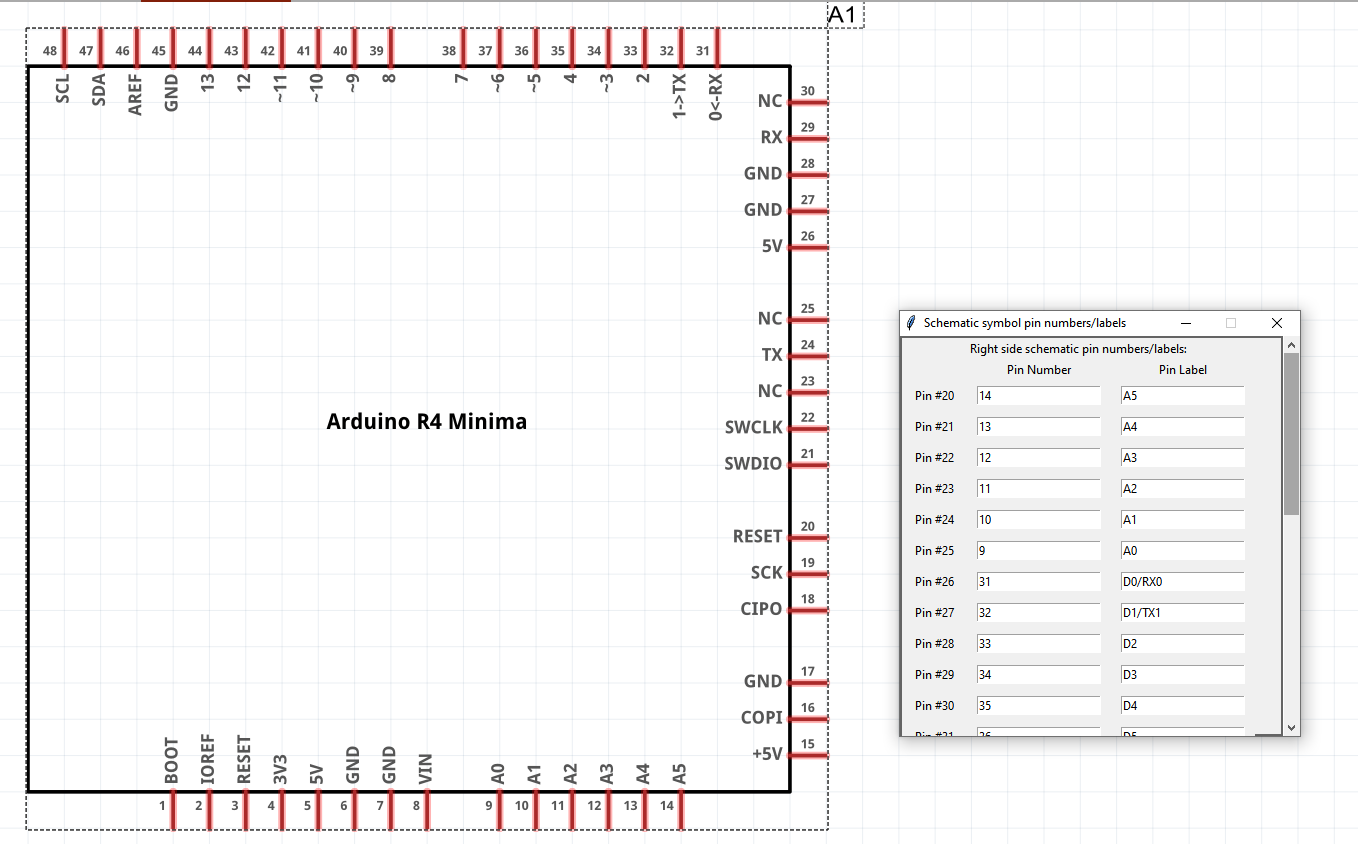
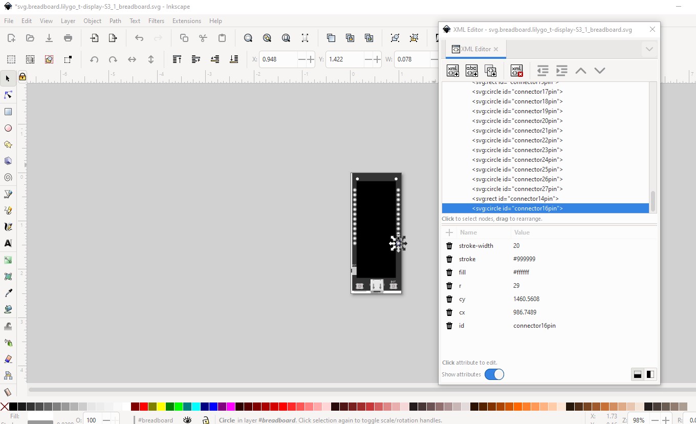
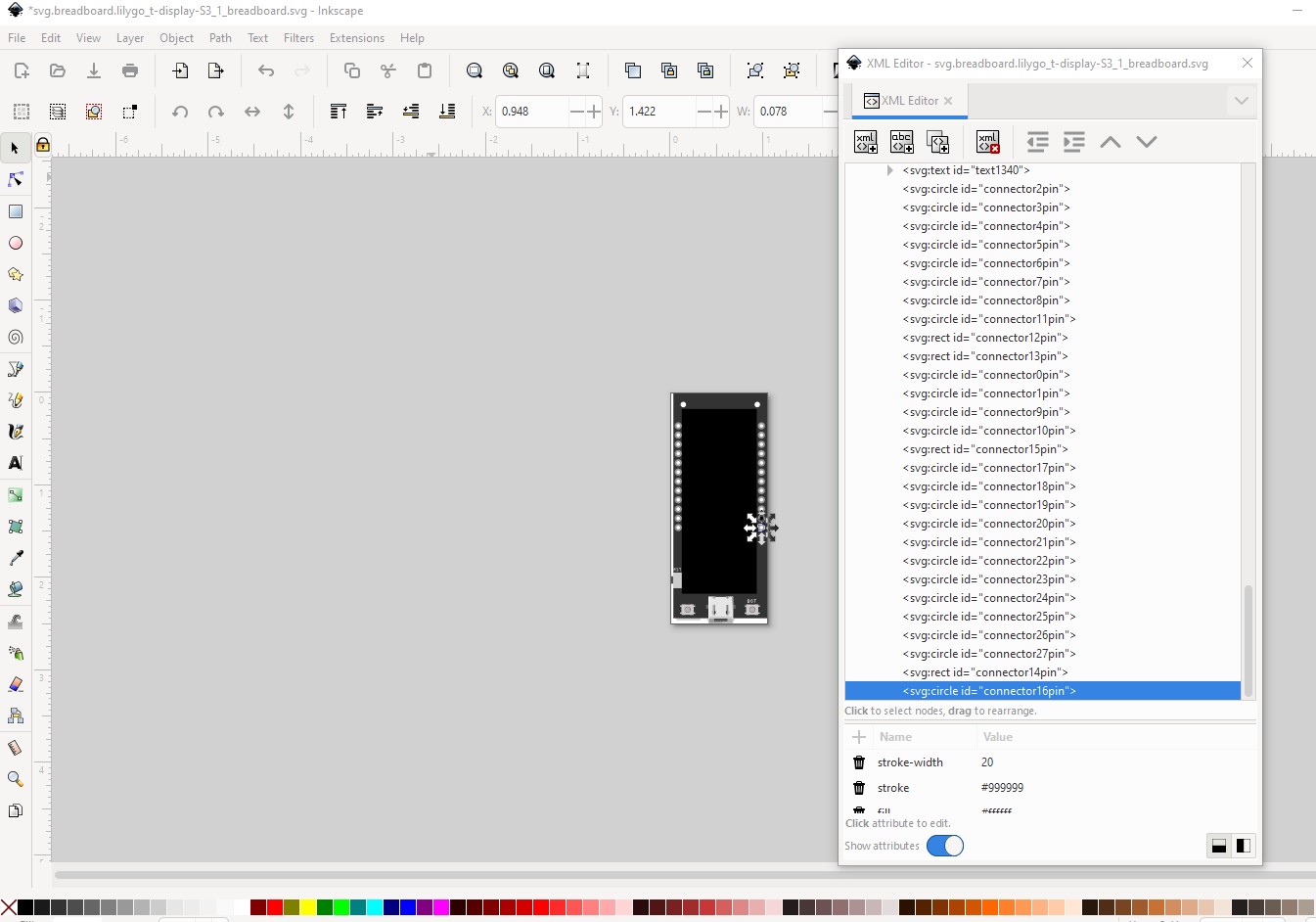
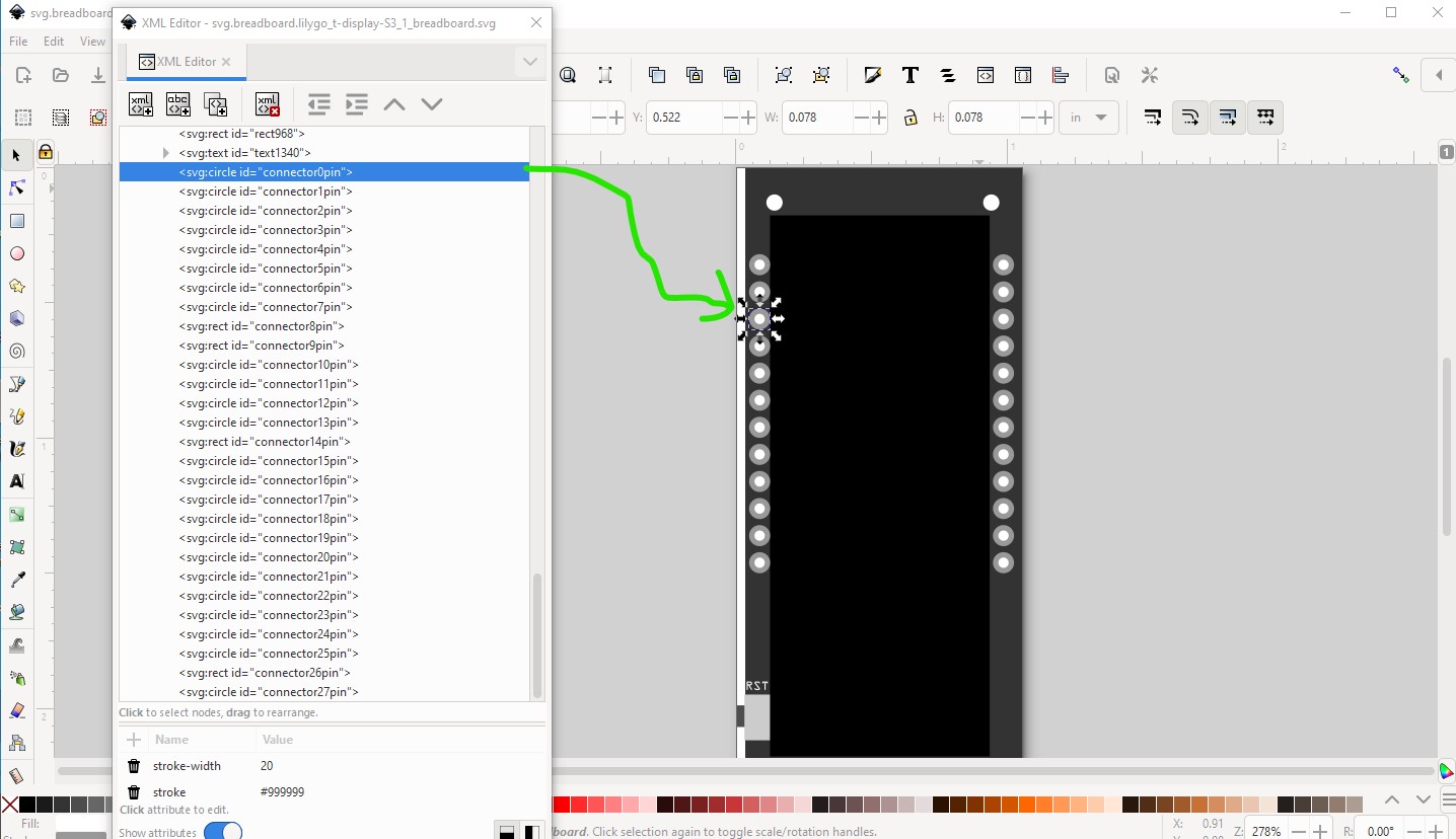
The extension starts with connector0 on the left side (assuming there are pins defined on the left!) followed by the bottom, right and last top. That means that you need to consider what schematic is going to look like when assigning pins in breadboard (assuming you start in breadboard of course!) The extension will create a pin for ever connector, so you need sufficient room for all the connectors (even if you intend to overlay multiple connectors on top of each other later!) So lets start by making a schematic for this part (which is available here)

(this is an svg. Right click on it and select save image as to download the svg!)

svg.breadboard.lilygo_t-display-S3_1_breadboard

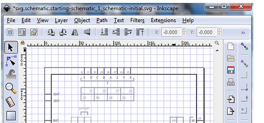
to do so I need to first figure out the connector layout. Here I chose to do the simplest and did it in order starting with connector0 on the top left for 12 connectors, continuing with 4 connectors on the bottom then 12 connectors on the right. So open the schematic svg file in Inkscape like this:

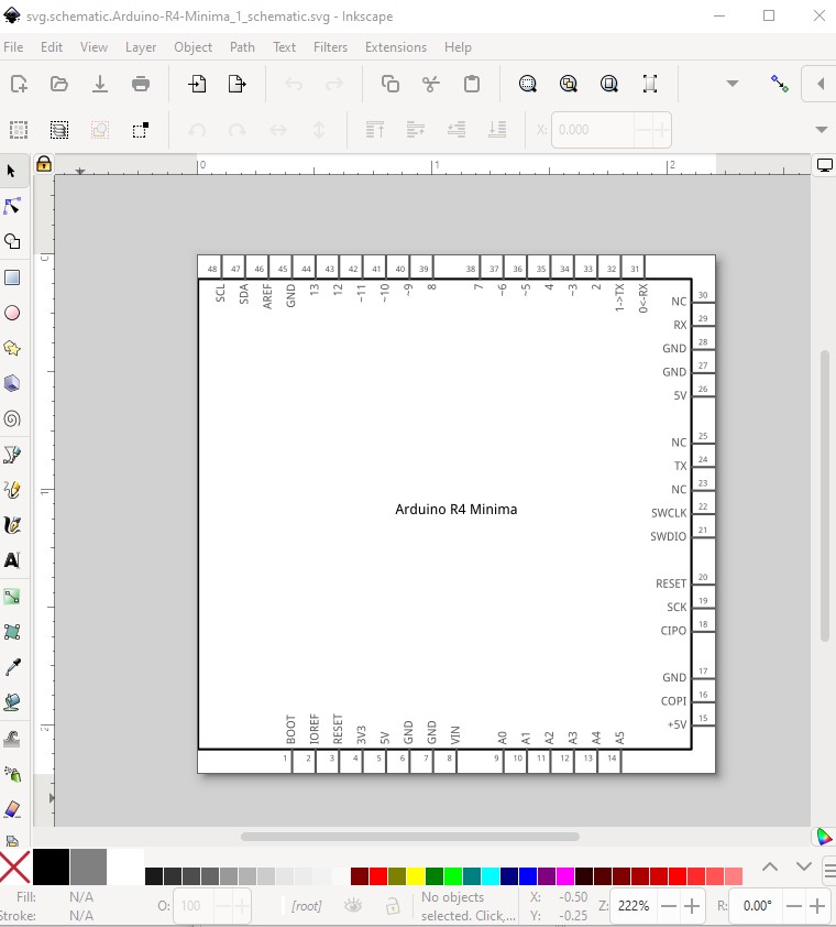
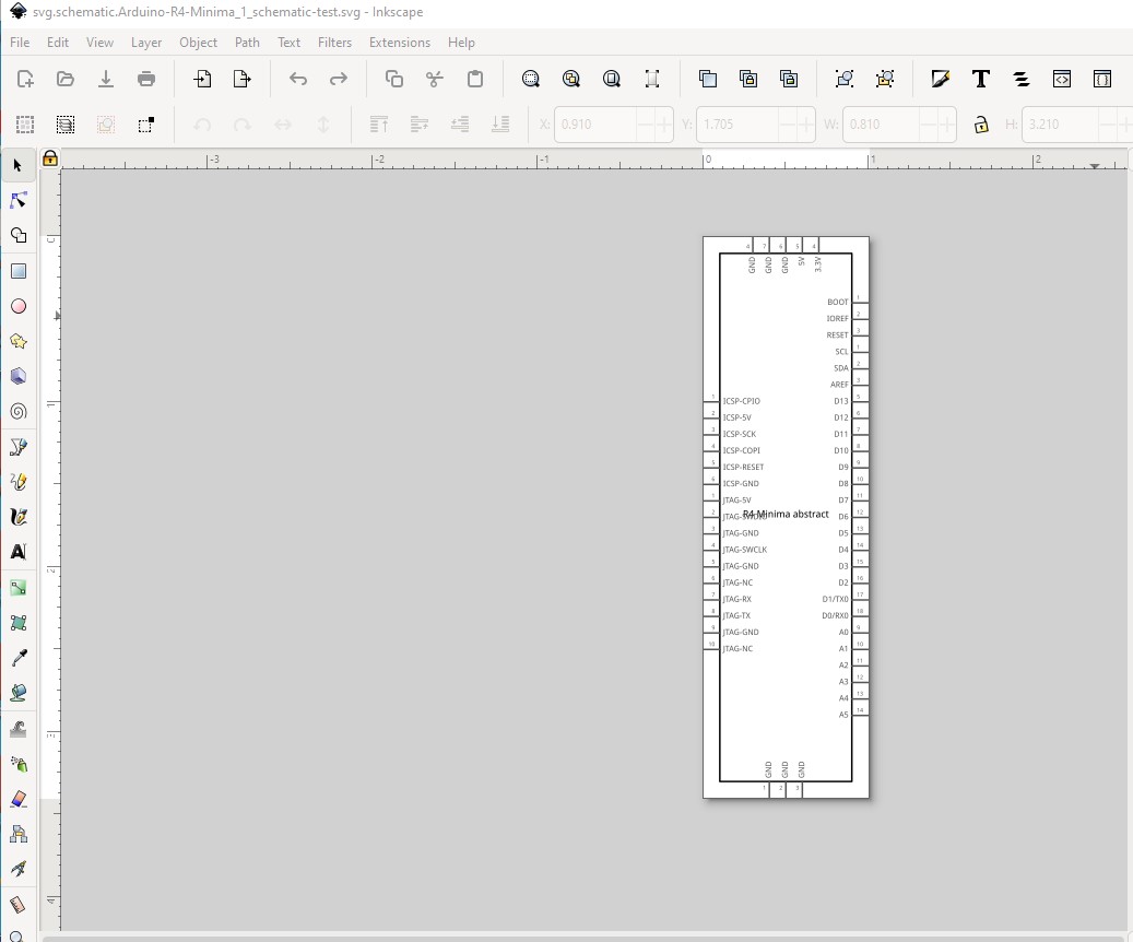
This is the final schematic we are aiming for (as I just made this part for someone.) So first delete the current schematic as the extension will add the new schematic without deleting anything that is already there!

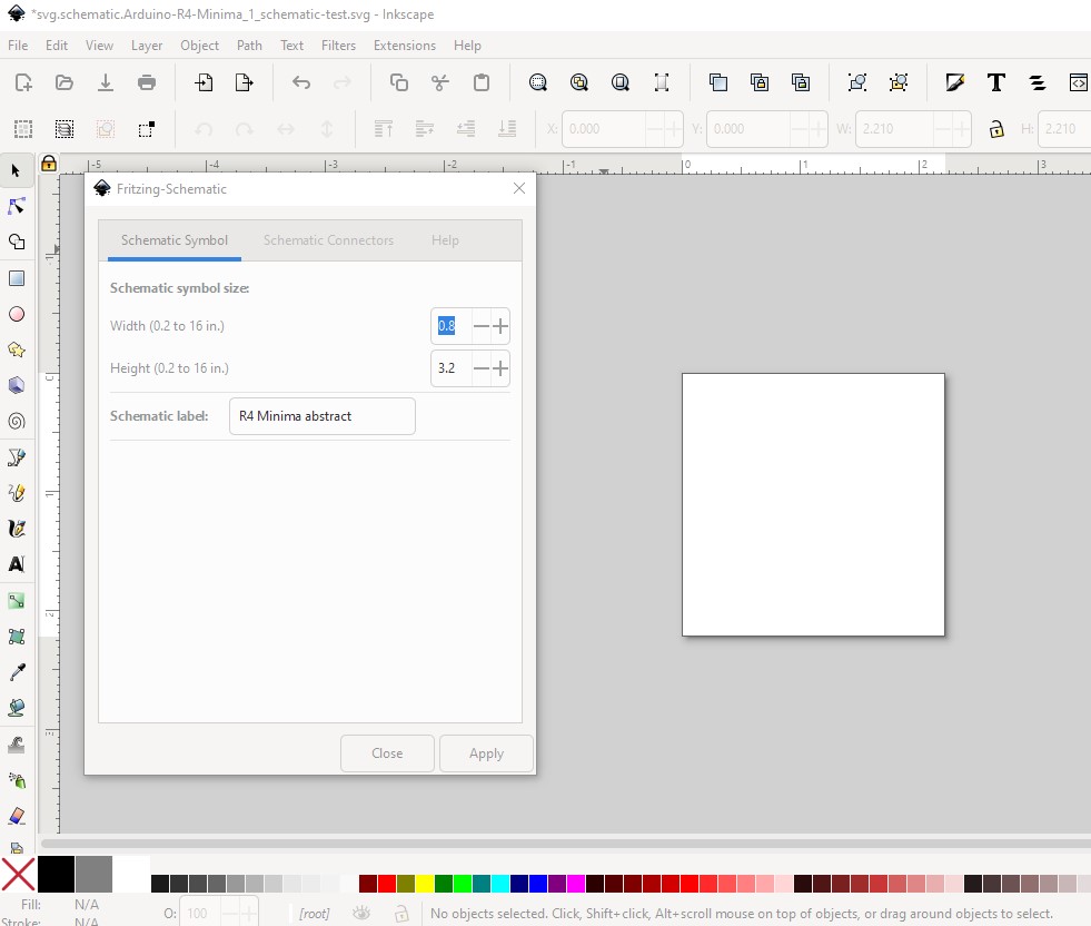
Then start the schematic extension like this:

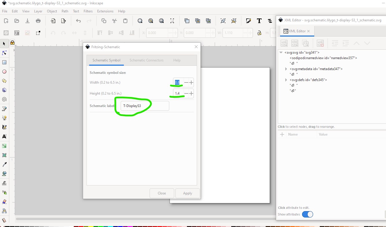
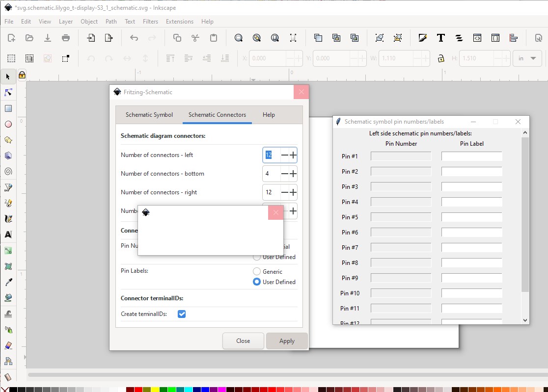
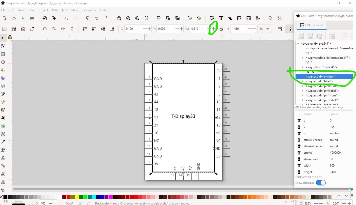
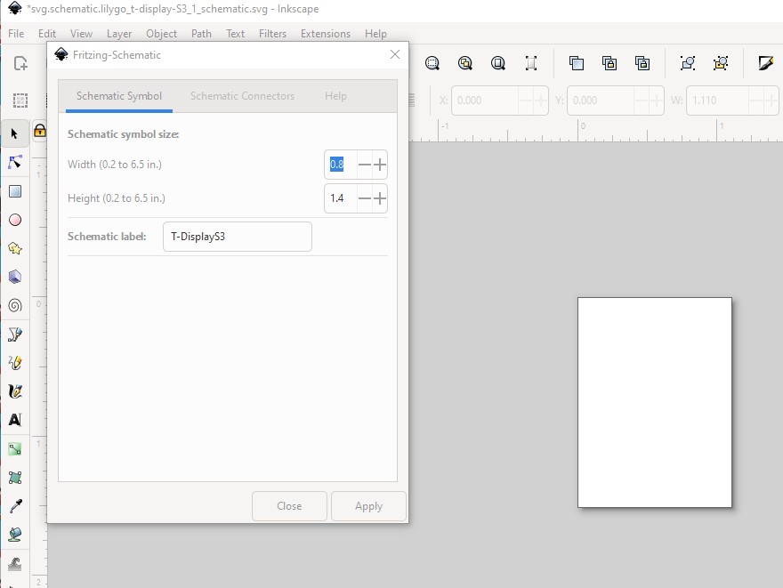
then switch to the schematic symbol tab and set the Label (only one line allowed) and the height and width of the schematic. Note each connector takes 0.1in so you need the height and width to be max_connectors + 0.1in, if you have too small a space you will get an error message. Here I used 0.2in more than the 12 pins (i.e. 1.4in when only 1.3in is required) for height.

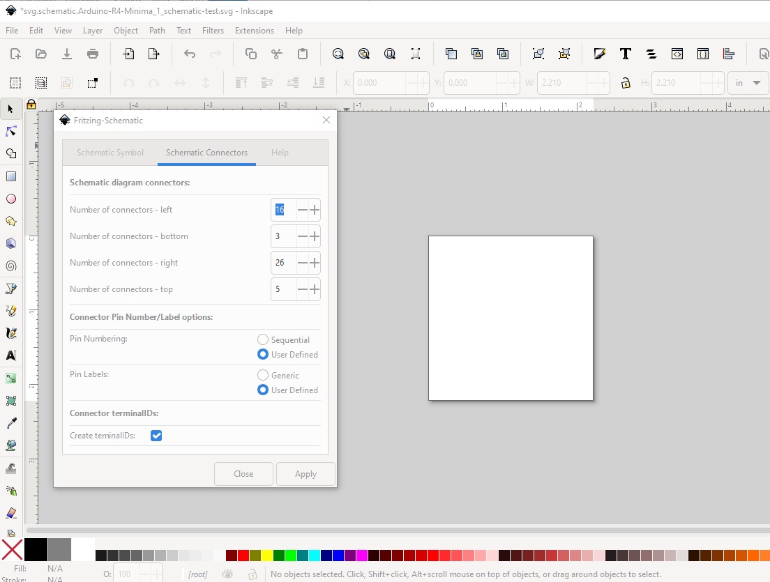
Now change to the Schematic connections tab

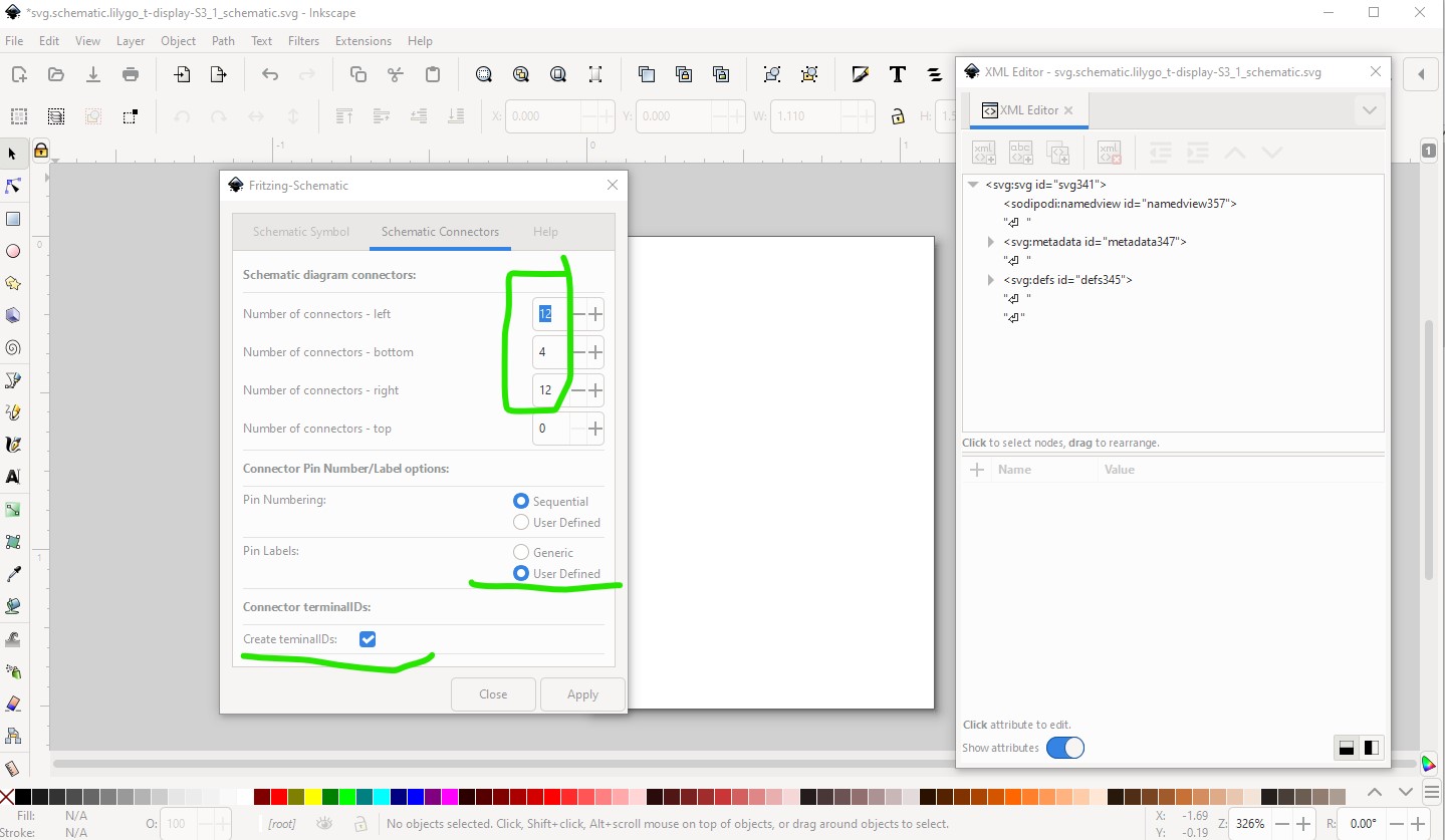
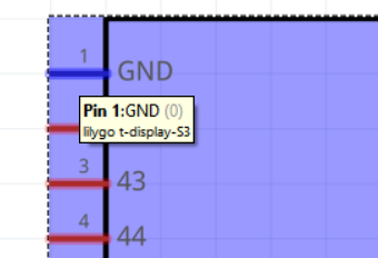
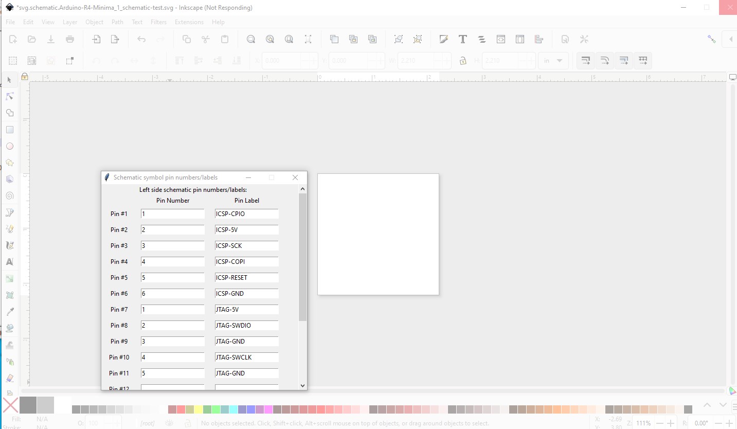
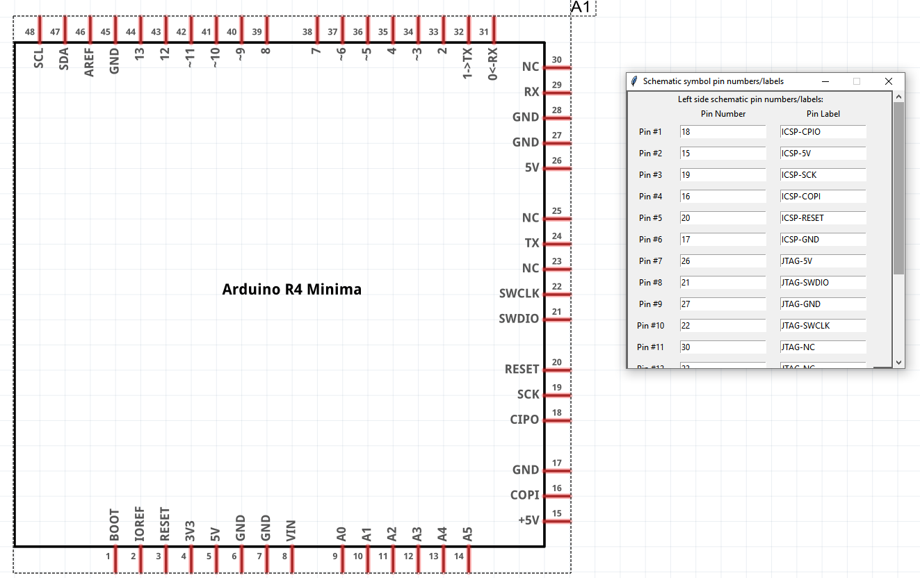
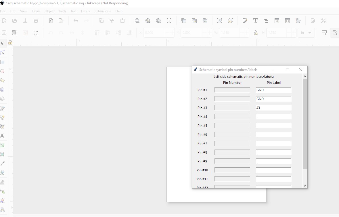
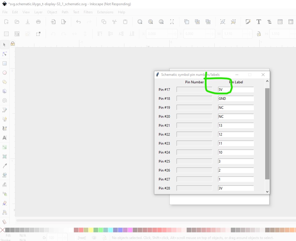
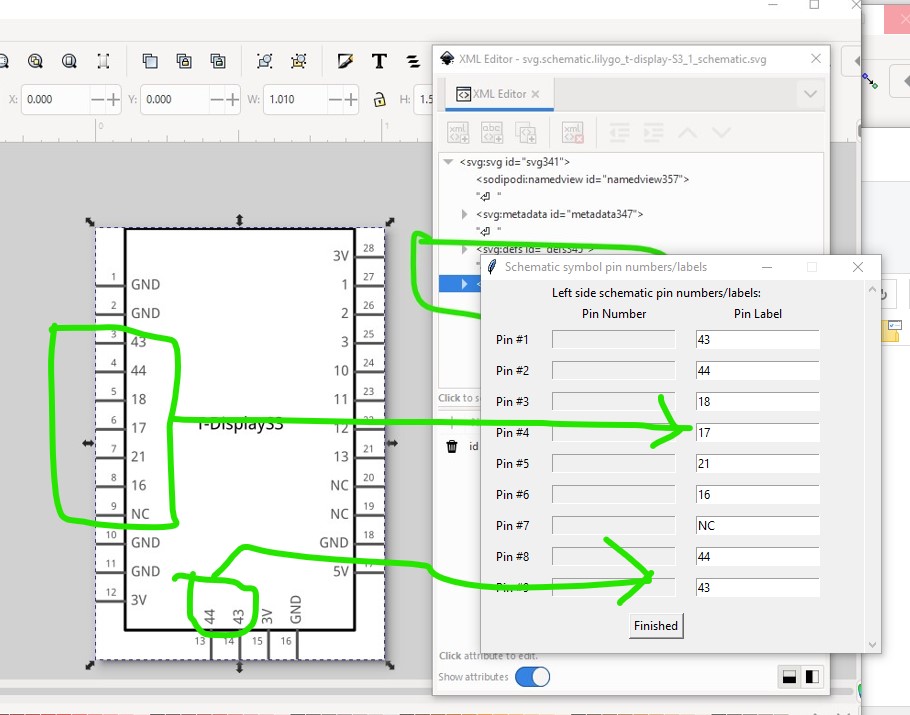
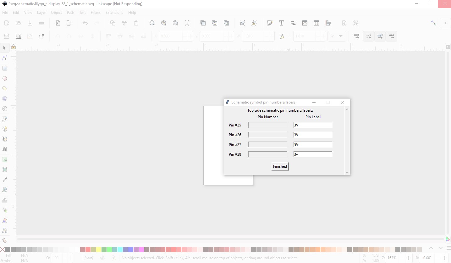
Here you need to set the number of connectors on each side of the rectangle as well set the Pin Labels to User Defined (other wise they will be set to the pin number, i.e. the connector number + 1) and insure the Create terminalIds box is checked as you always want terminalIds. Now you are ready to hit apply which lets you set the pin labels like this:

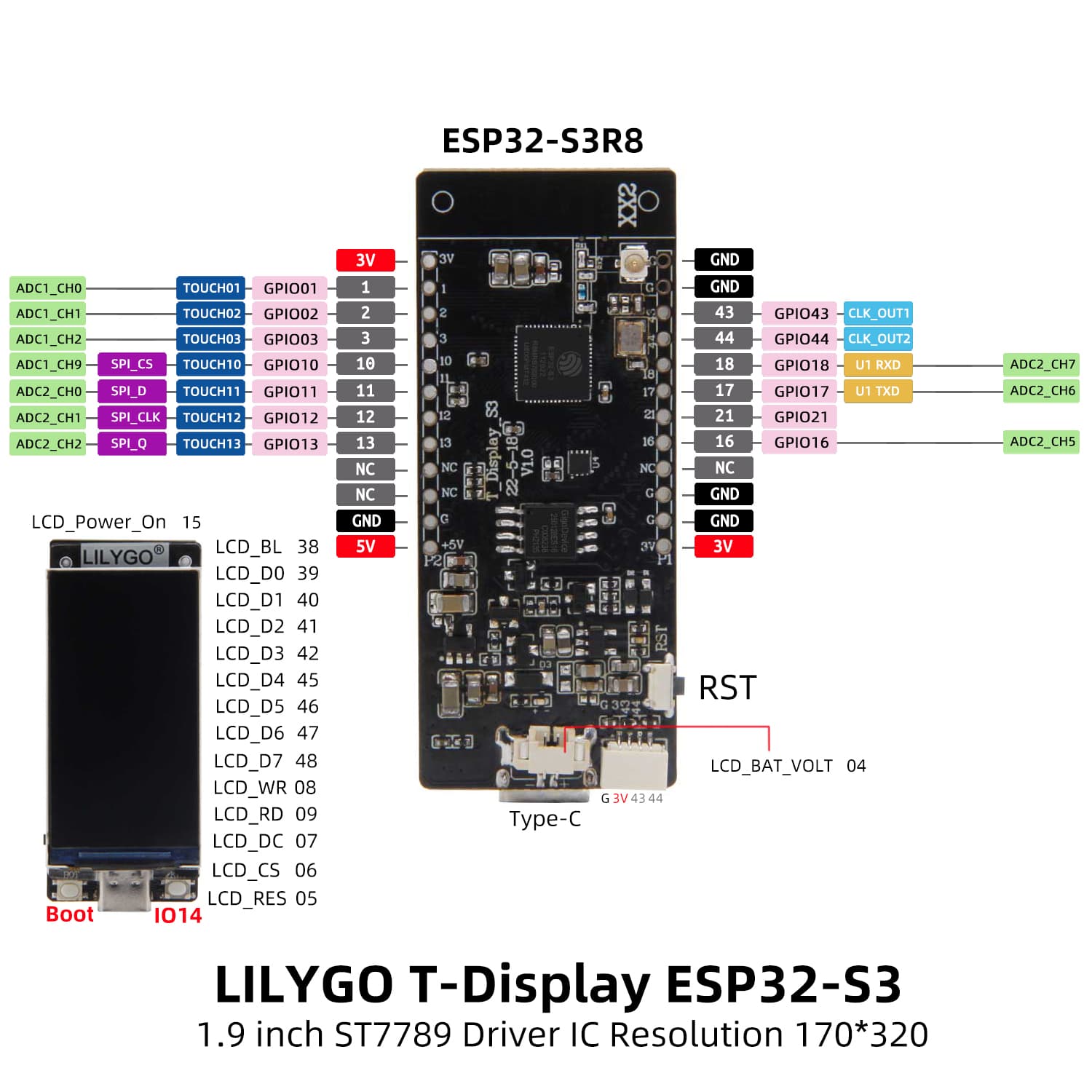
note this picture is from the bottom of the board so the pins need to be swapped horizontally in this case.

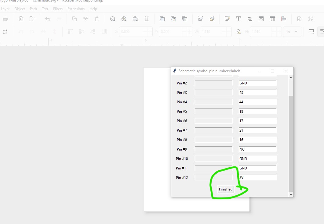
Now enter the text for the pin labels one at a time.
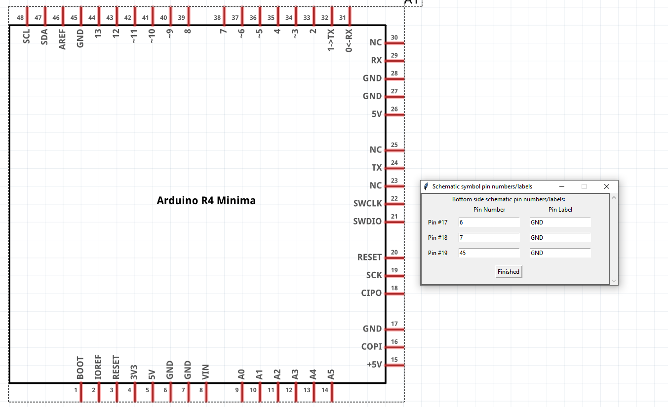
then click finished

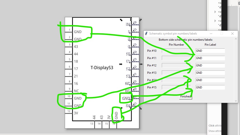
which brings up the bottom 4 pins (starting from the right) so set them

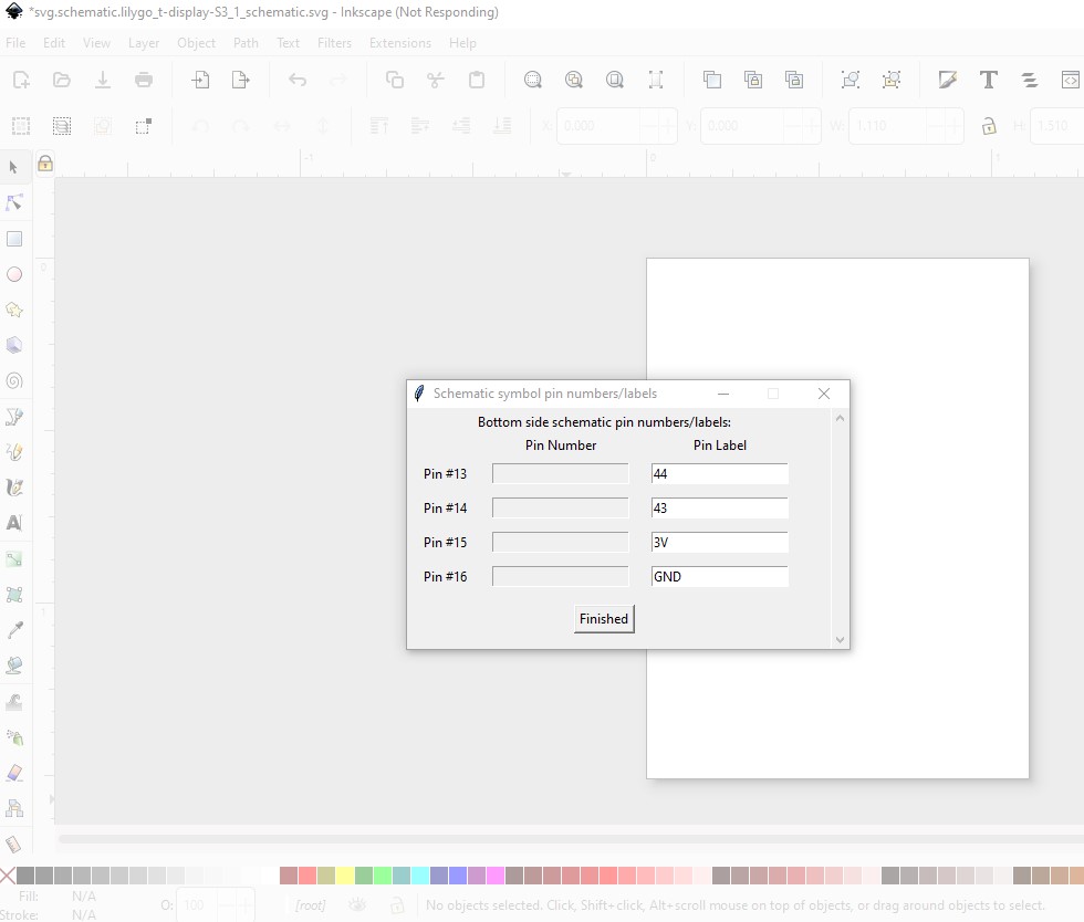
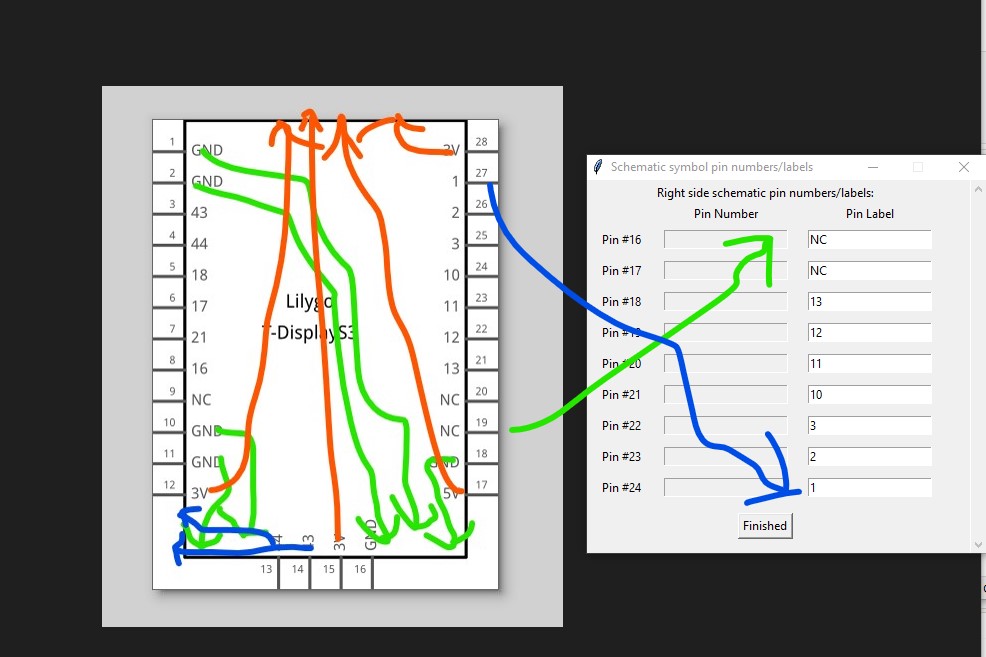
and click finished to bring up the right side connectors

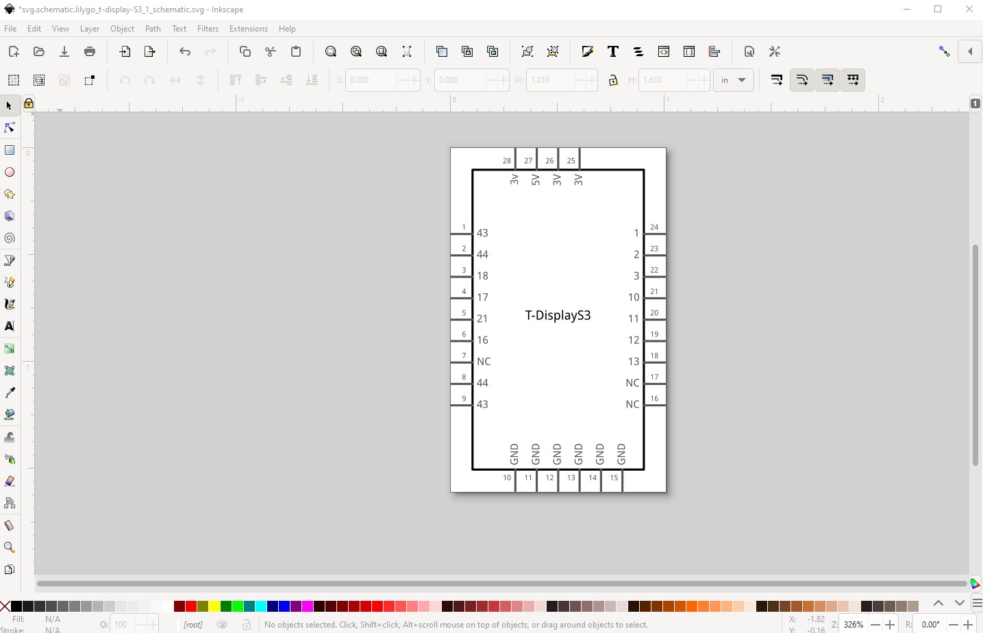
of note here is the pins start at the bottom of the board not the top as was true of the left side, so 5V on the bottom of the image is the first pin. Clicking finish here creates the svg like this:

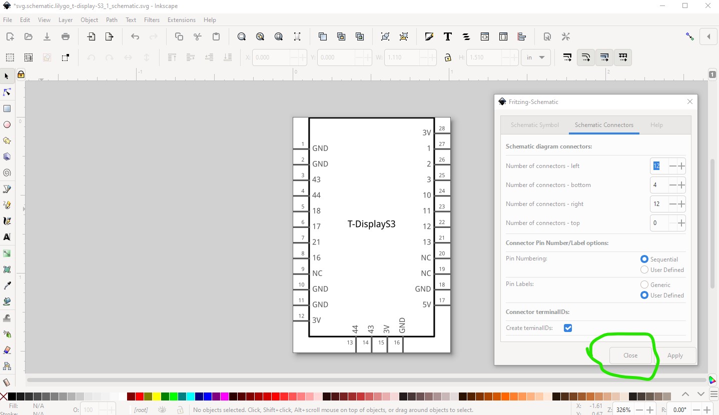
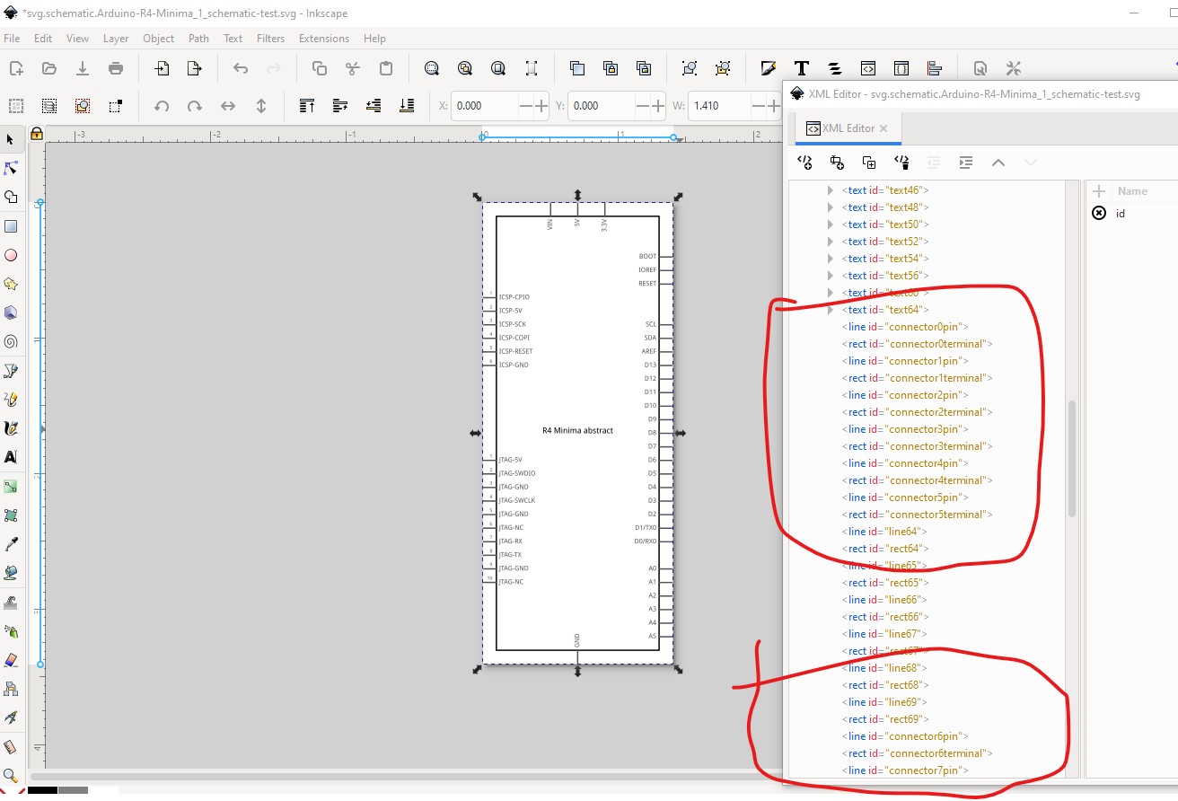
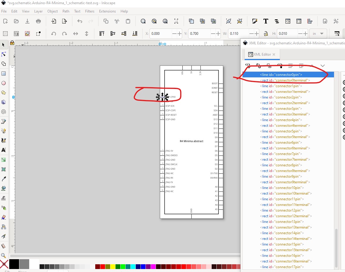
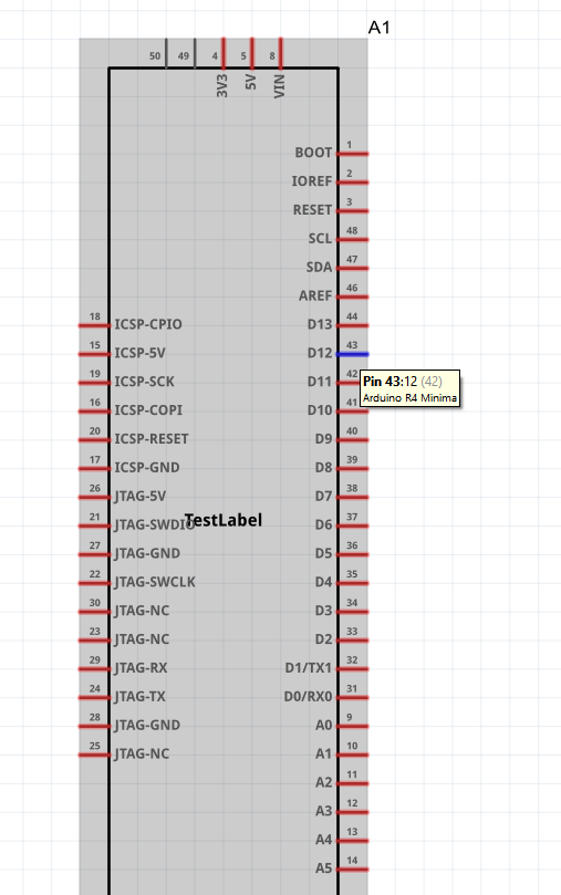
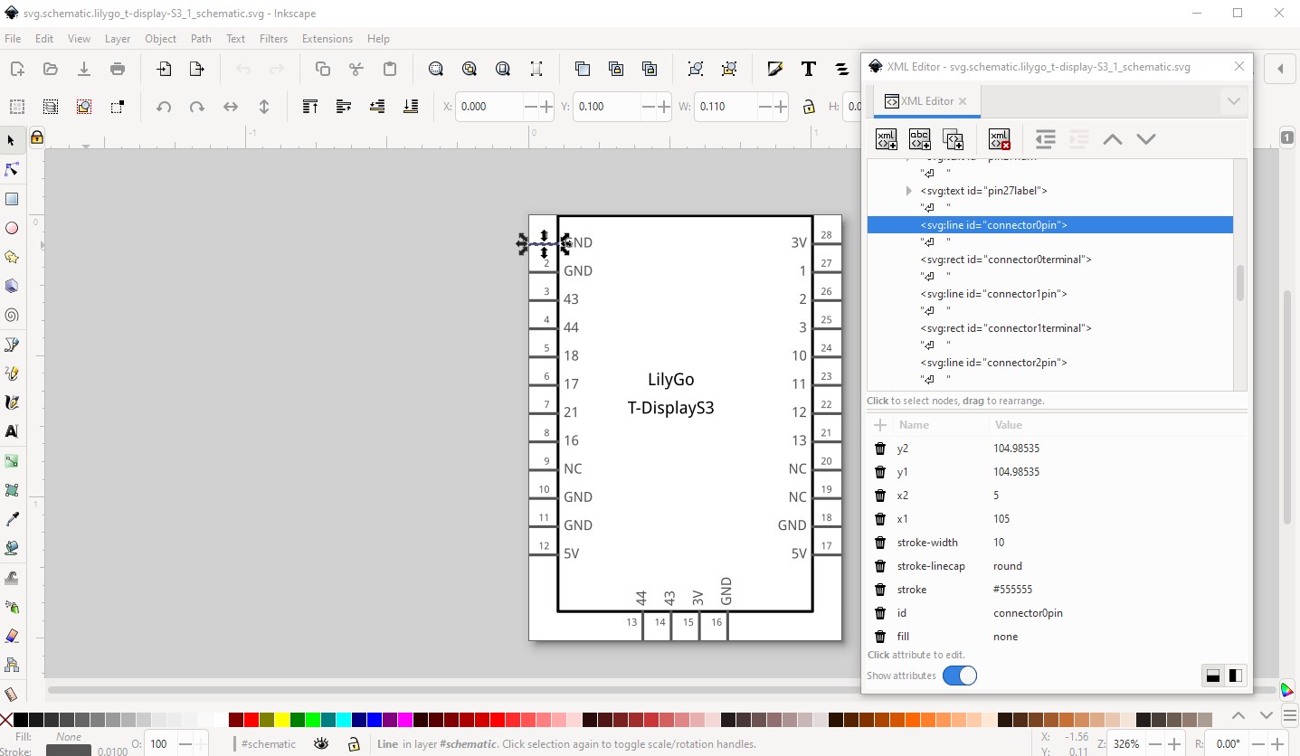
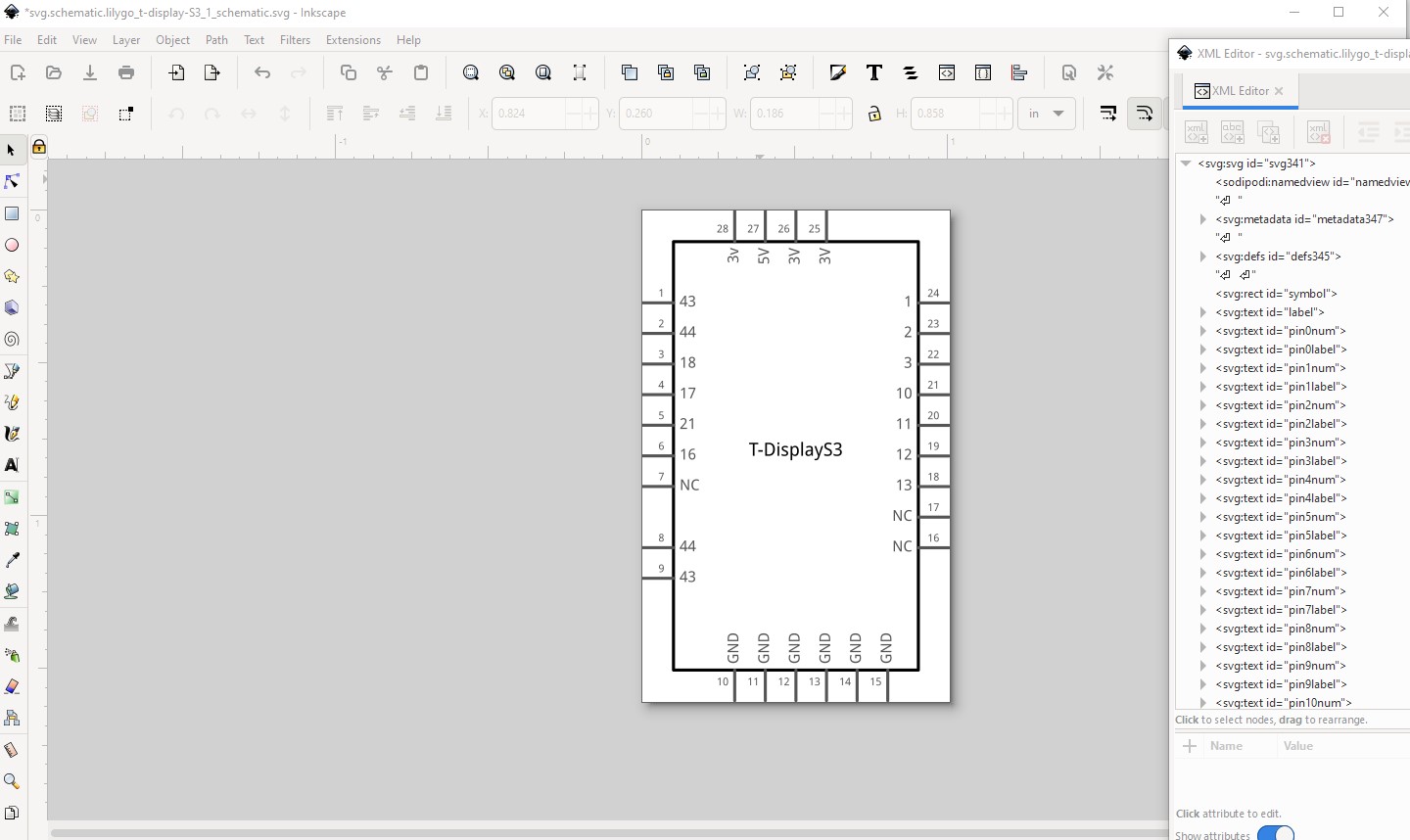
now click close to exit the schematic extension. Now I need to ungroup the schematic group in order to move some of the pins around. This is not uncommon when you guess at how the schematic is going to look.

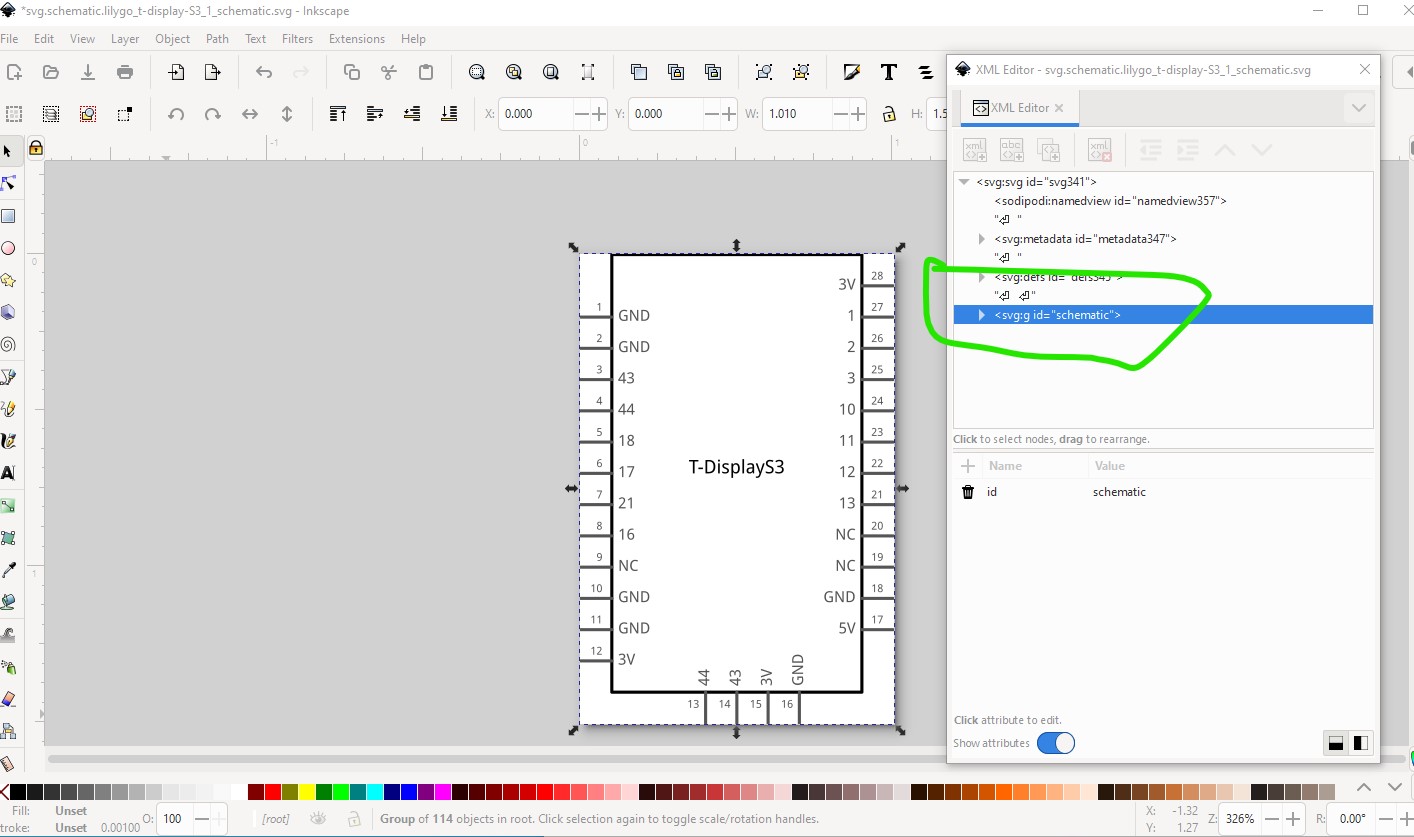
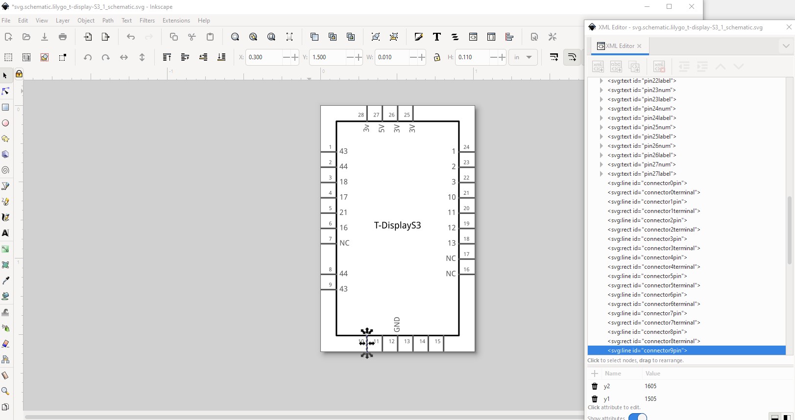
To do so click on the schematic group and either click on Object->ungroup of hit Cntrl-shift-g on the keyboard to ungroup. Now you can move the schematic like this (first insuring the tool bar is set to in) select all the right side connectors and move them 0.1in right by clicking on the x tool bar increment (which will move the selection 0.1in right)

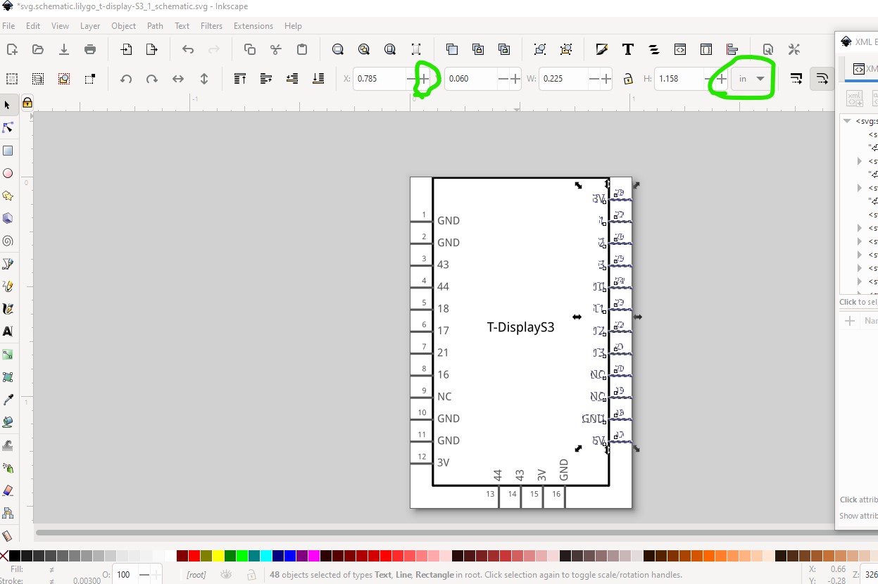
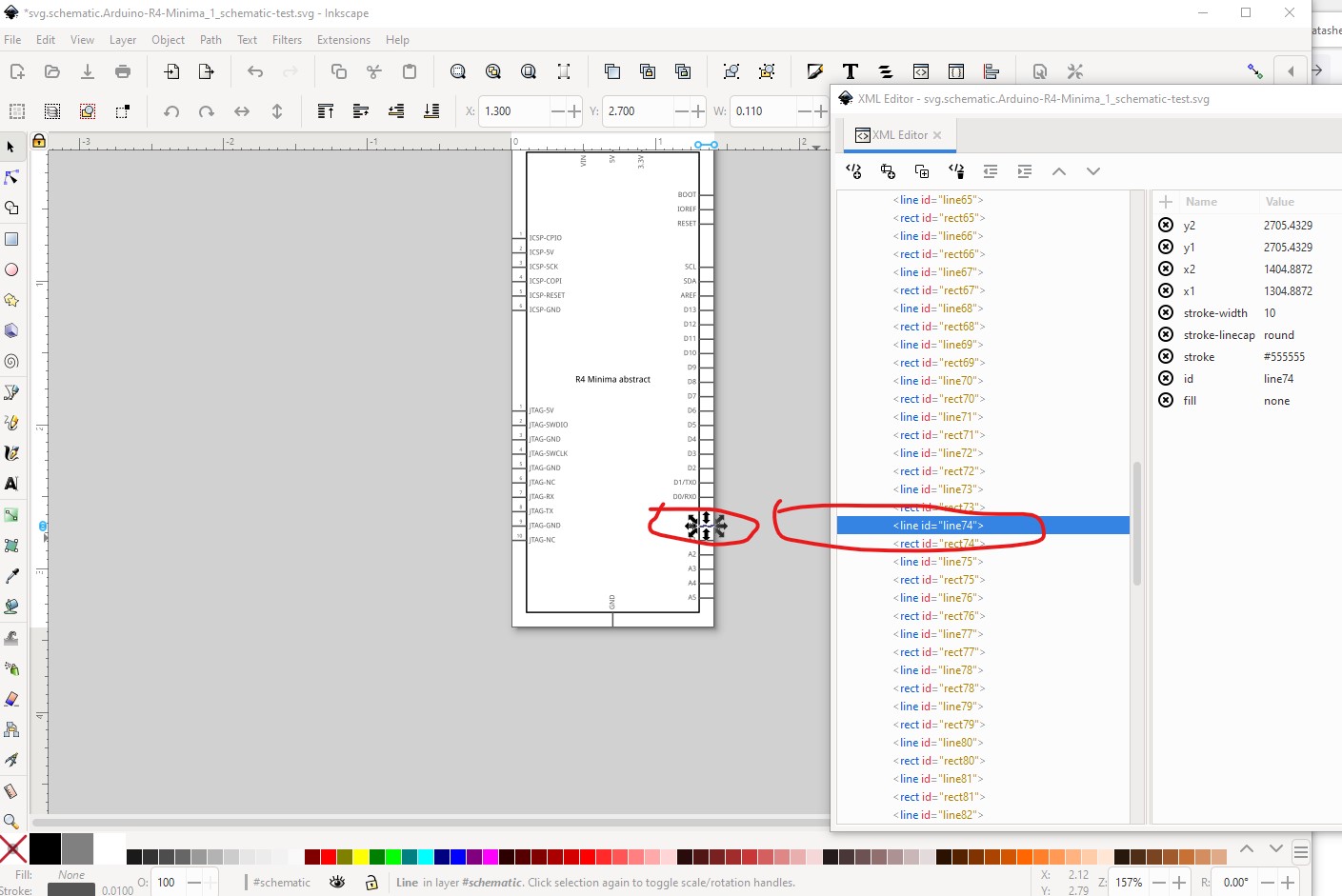
then select the rectangle and click to increase the width by 0.1in to make the rectangle be equal on both sides of the bottom 4 pins.

then select all the left side pins and move them up 0.1in to match the ones on the right

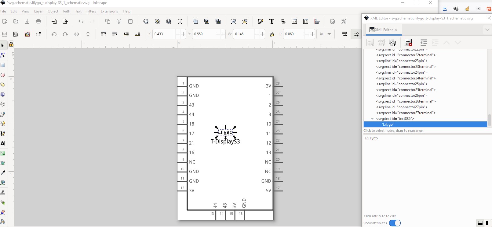
Now duplicate the T-display-S3 label and move it up 0.1in in y and change its text to Lilygo to add the extra label line (repeat as needed for more label lines!)

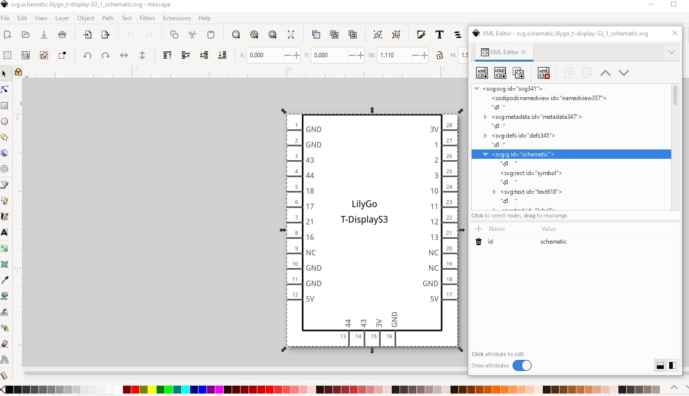
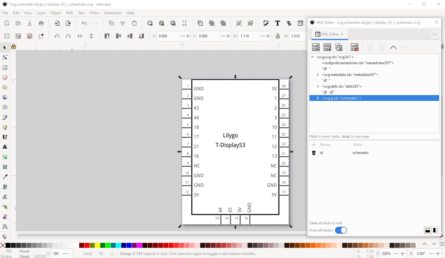
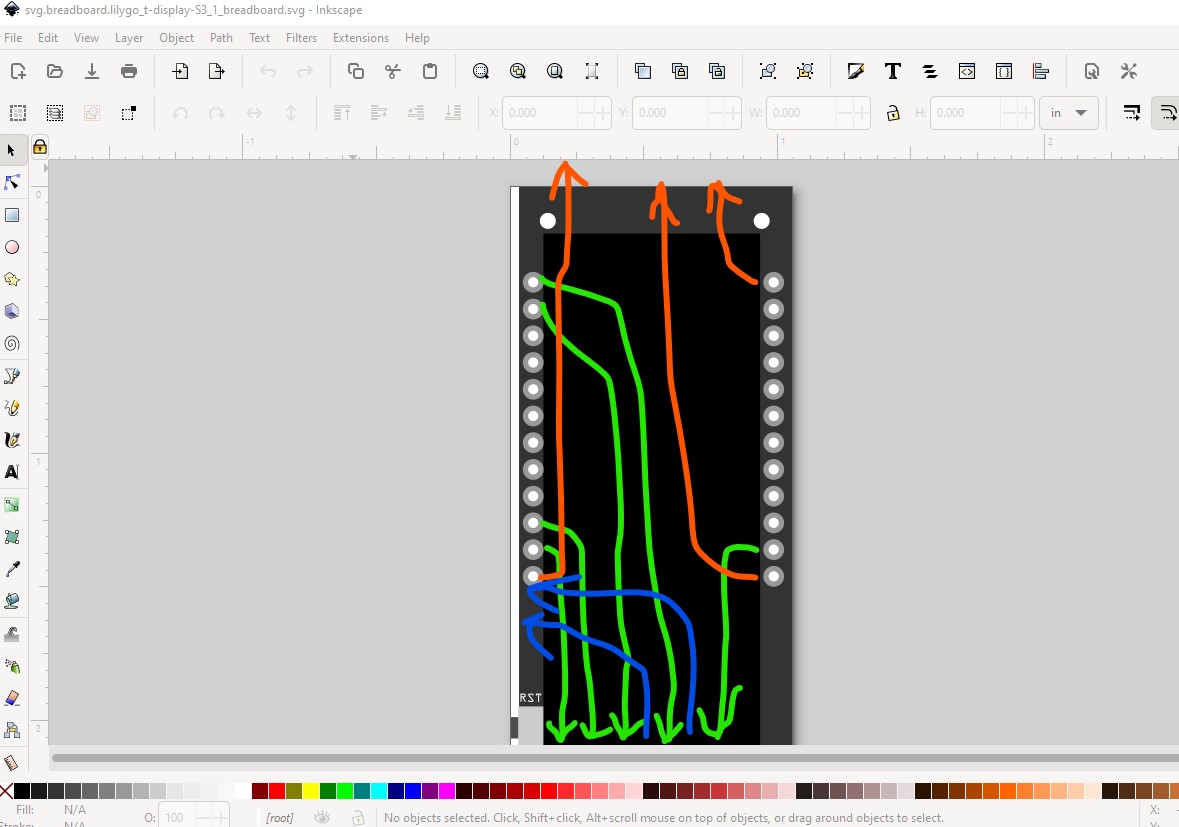
This completes the changes to the schematic svg, so Edit–>select all, Edit->resize page to selection, Object->group and set the layerId back to schematic then File-> Save As and set the type to plain svg and save the resulting svg. This has created the same svg I used on this part. Now I am going to make some changes to make the schematic meet the KiCad schematic recommendations (which it has been suggested that Fritzing use as well.) To do that I need to make some changes in the breadboard svg to to change the pin numbers. Essentially the power pins should move to the top of the schematic and the grounds to the bottom (with multiple pins overlaid on one another to create a single pin for a connection.) To make that work with the schematic extension we need to make some changes in breadboard (and then do some manual editing in the schematic svg.) Since the breadboard svg has no labels, I used schematic to indicate what pins need to move and where and used that to change breadboard. Basically the grounds all move to the bottom, the power pins all to the top and the two debug data pins to the left side like this:

On schematic (which has pin labels) that looks like this. We need to move the ground and power connectors to a different order by rearranging the sequence of connectors like this:

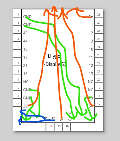
In breadboard (where we need to start) that looks like this:

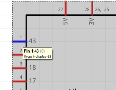
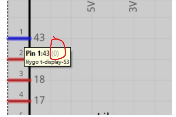
first the top two ground pins need to move after connector11

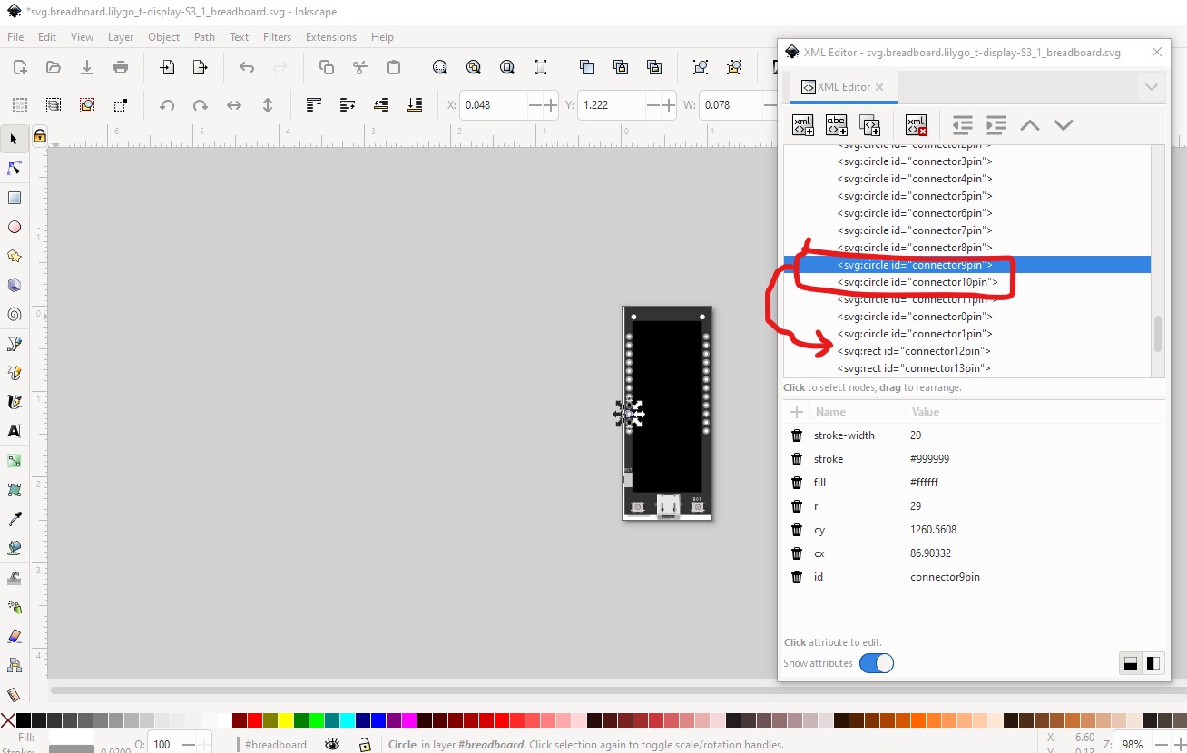
then connectors 9 and 10 need to move after 0 and 1 like this

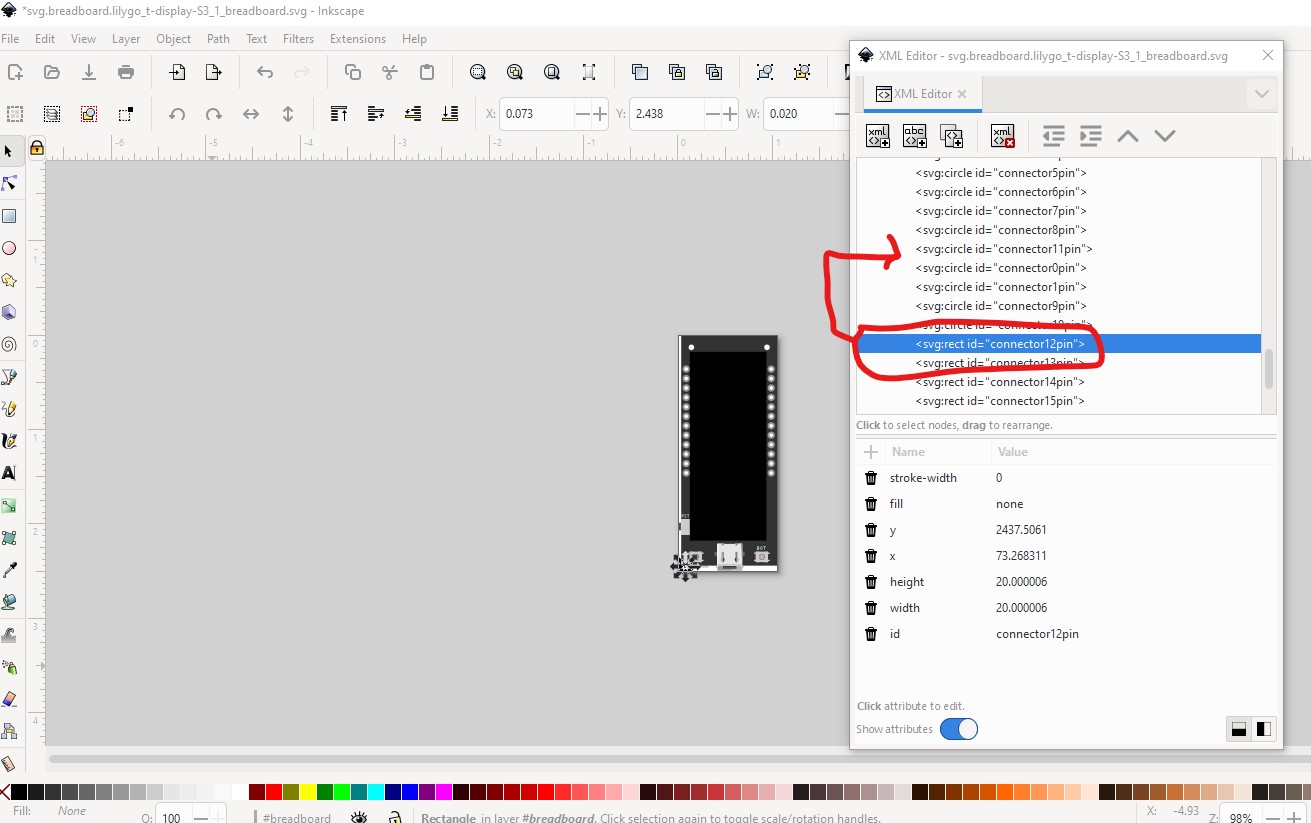
then connector 12 and 13 (the data pins for the debug port) need to move after connector 11

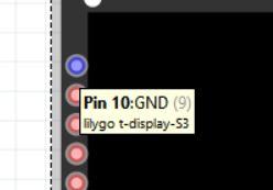
connector15 (GND) stays where it is on the bottom of the board.

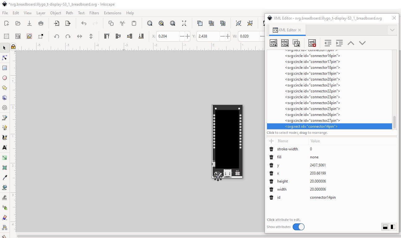
connector16 (5V) needs to also go to the bottom of the svg to be at the top of schematic.

and we are done as all the connectors are in the correct place (if not the correct order!)

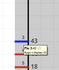
you likely have to manually renumber the pins to start at connector0 and go to connector27. I have a script (not yet clean enough to publish) that will do this automatically if the pins are at the bottom of the svg as they are here. We need to end up with this:

Now we are ready to redo schematic. On the left side we need 9 pins (connector0-8) we want to add some more (probably 10 to 12) to the height to allow for spaces. Bottom needs 6 pins for grounds (use 8!) Right is smaller than left so will be covered by left and totals 9 pins the top has 4 pins. So we now have enough information to set the schematic extension parameters to make schematic. Again start from an empty schematic svg

I left it at 0.8in by 1.4in

and changed the number of pins on each side to the new values above

then apply and set the pin names

then do the grounds on the bottom

Then the right side (starting at the bottom!)

then the 4 on the top

then click finished to create the schematic svg which looks like this

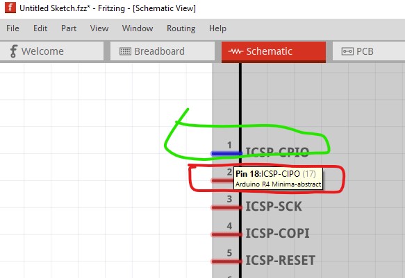
which we now need to edit, so ungroup it then move the left side to separate the 2 debug pins from the rest of the connectors and move the right pins up 0.1in to match the left.

Now we need to move the ground pins to all be on top of each other like this first remove all the GND labels except 1.

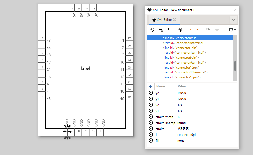
first select the pin to be moved and change its stoke from #555555 to none like this

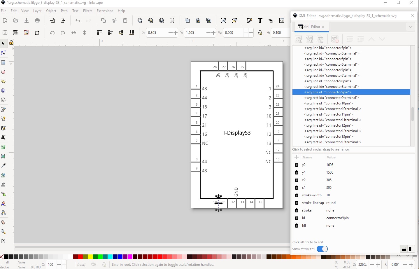
then move the pins all on top of the center pin like this (select both the pin and the terminalId for the move!)

then move it left by 0.2in (by increasing x in the tool bar twice) to put it on top of the pin with the label

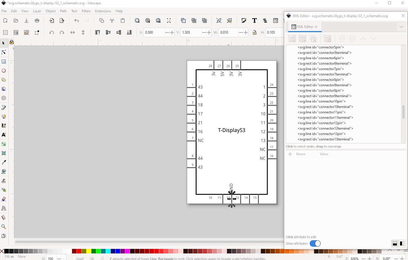
repeat for the rest of the GND pins to end up with this

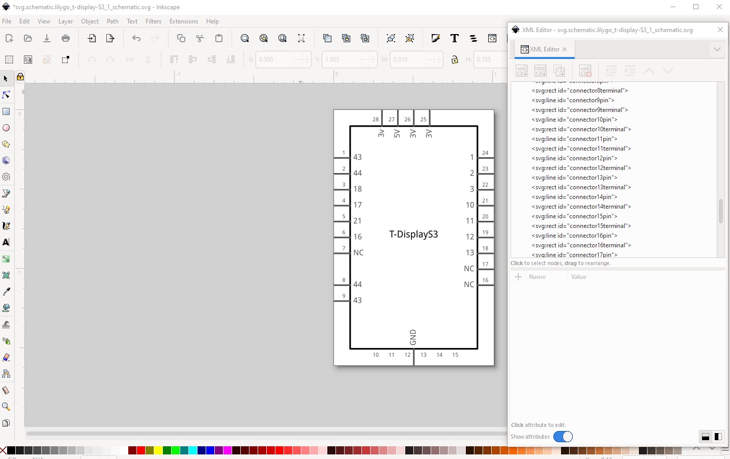
now add commas to the pin numbers and move them in towards the pin a bit (alternately remove the pin numbers completely if you want)

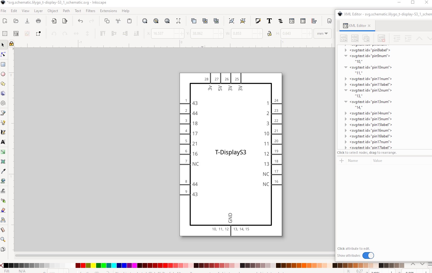
Now do the same for the 3 3V pins on the top of the svg and move the 5V pin to its correct position

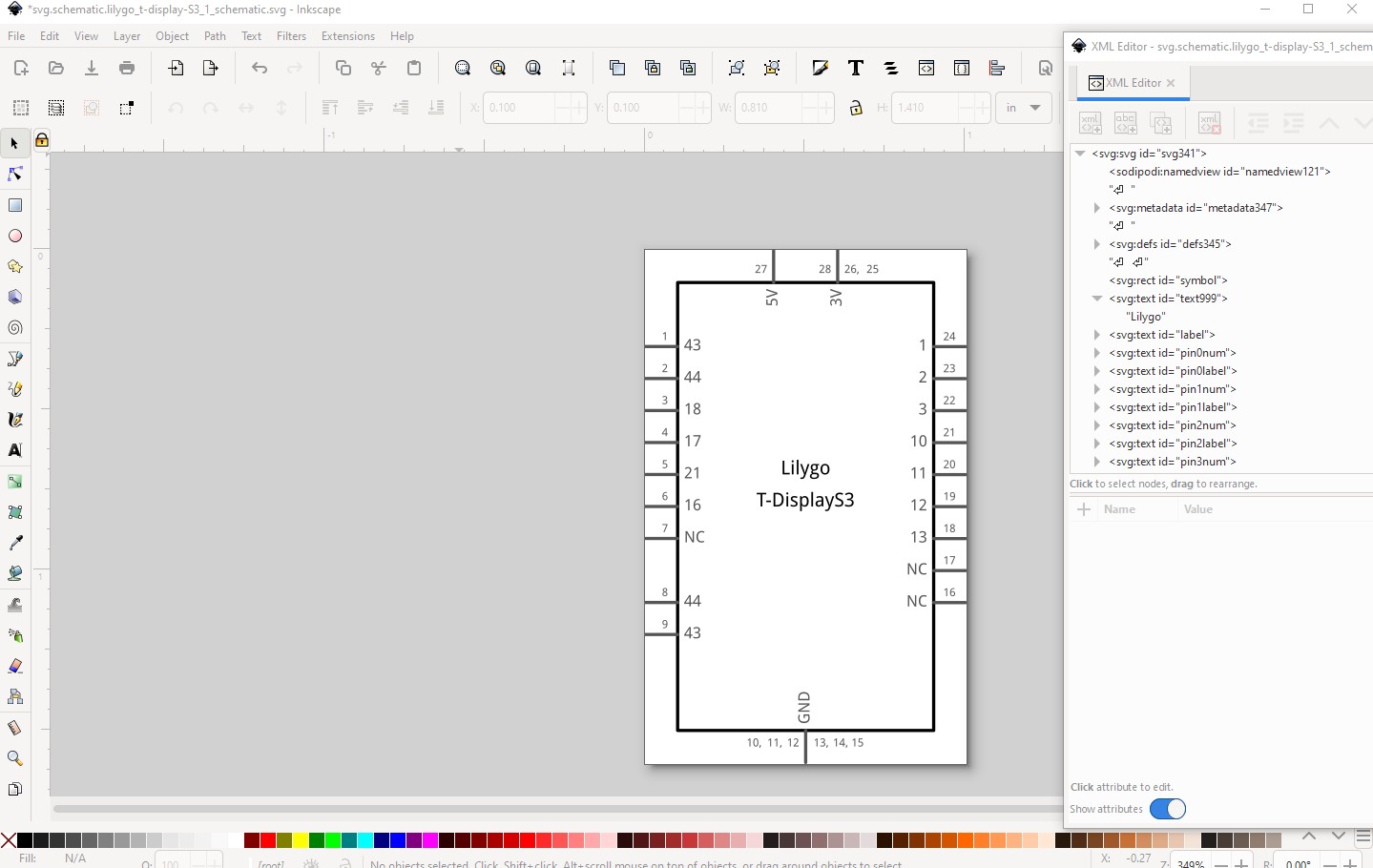
and we are done schematic and can now do the Edit-> Select all, Edit->Resize page to selection, Object->Group and rename the group to schematic before saving as plain svg to complete the schematic svg. Now we need to adjust the pcb svg to match the pin numbers in breadboard and then adjust the fzp file to reflect the pin number changes and we are done except for testing. I chose to be lazy and copy the breadboard svg over top of the pcb svg and then edit breadboard to replace pcb (as breadboard has the pin numbers in the correct place) like this

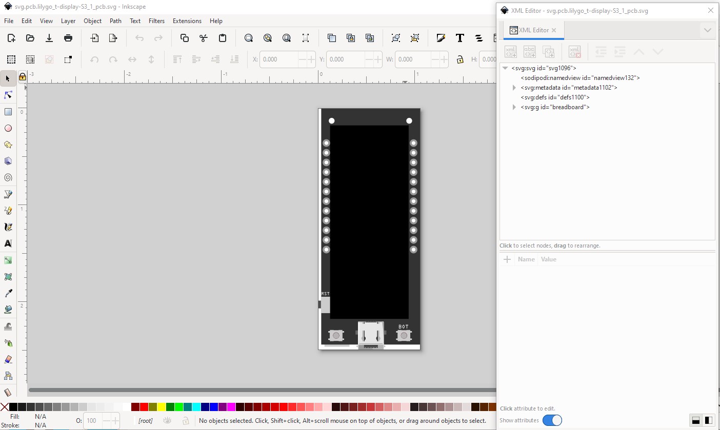
then ungroup the svg and delete the unneeded by pcb parts.

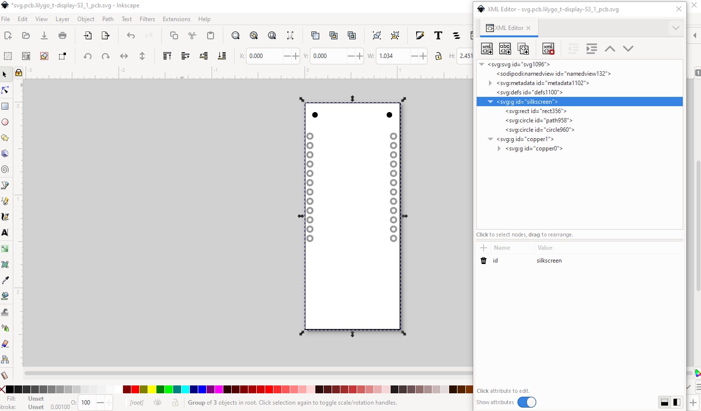
then changed the color of the pads in the svg with a text editor.

On to the fzp file. Here all the needs to happen is the description field needs to change to match schematic so use a text editor to change the descriptions. We also need to change the 4 debug pins from male to female and adjust the bus definitions to match the new pin numbers and then the part is complete.

lilygo_t-display-S3-modified-sch.fzpz (8.7 KB)

Thanks for an excellent tutorial, @vanepp .

I am wondering if the process to create schematic symbols could be simplified. Maybe I am wrong, but could be possible to use the “user defined” option for the pin numbering to avoid to reorder the connectors in the BB SVG? I will explaon how I would do it, please, tell me if there are some issues with this method.

  1. Create the BB SVG and assign a pin number to each connector. In this example, The first GND pins would be pin 1 and 2 and the label 43 would be pin number 3, etc.
  2. Use the Inkscape extension to create the final SCH symbol organized logically. Select User defined pins and labels. In the tool, create the left pins (pin 3 → 43, pin 4->44, etc.), create the bottom pins (pin numbers 1, 2, 10, 11, 16, 18-> all labels GND), etc.

If you do that, you will end up with this SVG:

Could that work? If so, it will save you some work or rearranging pins in the BB view. The pin numbers are arbitrary and the pin number one in the sch does not need to be the top left one.

Yes user defined will work. The down side is the underlying pin number is the connector number (to associate the correct pin) so the real pin number (which won’t match the displayed pin number) will appear when you hover over the pin. It is possible with enough thought that Randy’s extension can be changed to work more reasonably when we figure out what we want to do about schematic. That may be the best answer (although the issue with underlying pin numbers will still be present I expect.) One of the suggestions for changing how pins in hover mode are displayed may be the solution here (i.e. don’t show the real pin number) but there is a downside to that as well. It is often useful to be able to determine what pin in the fzp file this is from the hover display.

Peter

I am not getting what is the downside.

The schematic view shows how things are connected between the different terminals and each pin should contain its pin number, which is implementation specific (the same microcontroller could have the terminals at different pin numbers based on the package). See for example the atmega328p pinout:

In this example, I find the pin numbers shown in first part (in which the sch view replicates the order of the BB) correct. The pin numbers that show up when hovering the mouse are the real ones (“Pin 1: GND”), see below:
image
image

In the second part, where the sch view is logically organized, the pin numbers do not match the real ones, which I think is confusing. Pictures below:
image
image

If we use the user defined pins for creating the logically organized SCH view, would not the pin names match the order of the real part?

Yes, but the internal pin number in brackets (circled in red here) will be different than the pin name as it will reflect the connector number in the fzp file.

capture

and will change in a seemingly random way that no longer matches the displayed pin number. A fairly minor nit, but one to consider.

Peter

Sorry, I am not seeing the problem. I made the part with user defined pins (directly replacing the new svg schematic file in the lilygo_t-display-S3.fzpz part). The new part is here:
lilygo_t-display-S3-user-defined-pins.fzpz (8.7 KB)

And a screenshot of the message when hovering the mouse over the connector is shown below:
image

The pin number between parenthesis is the number of the internal connector, which is PinNumber-1 for all the connectors (in the highlited connector: Pin 1, label: “43”, connector number: 0). This is exactly the same in the parts that you made.

The error I was expecting (pin number mismatch) indeed doesn’t exist because the hover pin numbering is using the pin numbers in the fzp file and so appears normal. There are however other problems. To illustrate the problem I foresaw I redid the schematic for the Arduino-R4-Minima (the original part for which is posted in the forums.) and converted it to abstract using Randy’s Inkscape extension. Something (I’m not sure exactly what, possibly operator error) went very wrong.

Here is the starting schematic from the original part:

then the set up for the new schematic

set the pin numbers (which I expected to screw up but didn’t!)

which produced this schematic (which needs various mods.)

after making the mods (overlaying some of the pins) I discovered that the pin numbering is entirely broken (either due to an extension bug or operator error I don’t know which.) The connectors are not in order at the bottom of the svg and worse a number of pins which should have numbers do not, making the schematic basically useless without a lot of extra work (which the extension is intended to avoid!)

A number of the pins don’t have connector definitions (possibly because something I did caused duplicate connector labels which Inkscape won’t allow.)

to fix it I had to start with the breadboard svg and identify and relabel all the pins (a lot of work!)

connector0 got moved to ICSP CPIO which should be connector17 not connector0.

correcting all that results in this schematic

which is present in this part:

Arduino-R4-Minima-abstract.fzpz (30.7 KB)

but the experience indicates that abstract type schematics are going to be significantly more work to produce and test than my current “match breadboard” method. That isn’t necessarily a reason to not do it though. It is possible the Inkscape extension can be modified to make some of this easier as well (although I know nothing at present about Inkscape extensions!)

Peter

Hi,
I think you introduced the wrong pin numbers.

At the left, the original schematic symbol, which contains the pin numbers. At the right, I am creating the new symbol and filling the pin numbers and labels. Notice the pin numbers that you have to introduce are the ones that you have in the breadboard view. In this case, I would have sorted the BB view connectors in a different order (first the bottom headers, then the top headers of the arduino and then the connectors of the ISCP and JTAG). However, it does not matter too much, as they are arbitrary in Arduino boards.

Same for the grounds (bottom connectors):

The right side connectors:

The end result is working as expected:


This is the part (notice that I put 5 connectors at the top by mistake, there are only five):
Arduino-R4-Minima (1).fzpz (30.8 KB)

Perhaps, but that (AFAIK) shouldn’t have affected the connector pin numbering. That should only change the printed pin label and not affected the connectorId and terminalId fields which got corrupted. In addition the ICSP and jtag connectors do illustrate the original concern I had:

capture

Here I renumbered the ICSP connector to match the pin numbers for the connector (from 1 to 6 without regard to the underlying pin number.)
Hovering over the pin gets a different set of pin numbers (the first of which can be changed by changing the pin label in the fzp file, but the real connector number isn’t changeable!) which was my initial concern. To me this pin layout is more useful as it documents the layout of the ICSP connector in schematic to the part documentation, but it adds the complexity of the real pin number in the fzp file in the hover display (which a code change could suppress if we wanted, although I’m not sure that is a good idea either!) The bottom line is that we have decisions to make about how we want to do things and I think we need to document them before starting to make changes which is how the policy discussion got started. To me we need to create a document that details how all the fields in the fzp need to be filled in before trying to convert the parts to the new format.

Peter

No, the printed pin labels are always related to the connector number. When you set the pin number, the Inkscape extension sets the printed pin label to that number and also makes the connectorID and the terminalID as number-1. That is why if you define a pin order in the BB view, and then in the Inkscape extension you assign the correct pin numbers to each label, the SVG is can be use without problems, as you can see in the part that I uploaded.

In your part, you established the pin numbers in the SVG file of the BB view. There, you defined pin 1 as the bottom left pin, you continue with the headers at the bottom (A5 is pin 15), then the ICSP header (e.g., pin ICSP-RESET is pin number 20), then the JTAG, and then the top headers of the arduino. This creates a number for each connector of the part. You have to respect this order when you create the SCH file. If you do that, the resulting part is correct and does not take too much work.

In your part, the numbering in the SCH view is confusing as there are two printed pin labels called “1”. In a part, this means that they are phisically the same pin. I get that you where trying to specify the pin number for each connector, but in parts each connector needs to have its unique pin number. This is particular for Fritzing as other programs do not have assembled boards, only ICs.

My suggestion would be that we use a different numbering system. In this case, Arduino headers could be from pin 1 to pin 32 (bottom and top headers), the ICSP from pin 101 to 106, and the JTAG from 201 to 210. But this needs to be the same in BB, SCH and PCB views. When hovering over the connector, we would see the pin number, but I do not think this is a big issue as the pin numbers would be the same in all the views. Additionally, I would remove the printed pin labels from the SVG, which I guess it is an easy change to make in Inkscape. This is the way that the current Arduino Uno R3 in the core uses. As the pin numbers are arbitrary in an Arduino baord, we do not need to display them (in an IC, the numbering of the pins is standard and it is recommended to show them).

Is that really true when switching between a THT and SMD package? Those would have the same SCH, but do the pin numbers match?

Yes, the order of pin numbers in both packages is the same. The first pin is marked and the rest of the pins are numbered counterclockwise sequentially.

What is different is the function for each pin (the labels and name on the connector in fritzing). That can (and usually does) change. But they are two different parts. In fritzing, you would need two different parts. In both of them, the sequence of pin numbers would follow the same as in the package. And with the Inkscape extension you can easily create the logical sch symbol if you define the pin numbers manually (when creating the SVG file), without need to modify the order of the connectors in the XML editor.

AFAIK the user defined pin numbers in the extension are independent of (and are only the text label applied to the pin in the schematic svg.) The extension starts with fzp connector0 as the first pin (left if there are 1 or more pins defined in left) and increases til the end of the number of pins. The extension should not and normally does not change the order of the connectors (other than to move them in order to the bottom of the svg.) I am running Inkscape 1.3 alpha (an experimental prerelease for the adventurist to report bugs against) which may be why I got the screw up, or as noted I may have done something wrong although I have never before seen the extension screw up the connectors.

This is not entirely correct. The pins do have unique ids in Fritzing (connectorxpin) that exists in the fzp and defines the pin. As noted the extension starts with connector0 as the first defined pin and proceeds up from there sequentially in the order left bottom right top. If we are using an abstract model for schematic (and assuming the extension is working correctly) the pin numbers I used are fine. They define the pin numbers of the ICSP and JTAG connectors (as text labels in the schematic) which are then associated with the correct connectorxpin/connectorxterminal definition in the fzp file and thus the duplicate pin numbers are not a problem (and more importantly match the board documentation.) Specifically this one from the Uno R4 datasheet:

which allows you to see which physical pin on the connector is associated with the appropriate signal. As noted there is the issue that the values displayed by the hover on the pin in Fritzing will be the connectorxpin value (which will be different than the pin number in schematic although the description field in this case would be CSIP-pin name and thus possibly confusing.) My usual practice when doing that is to include in schematic a visual of the connector. I have done this but can’t immediately find an example in the 100s of parts I have made that shows this. Ah found an example in the schematic howto:

capture

although it has real pin numbers (identical to the Fritzing fzp connector) rather than the 1 to 6 of the actual connector which it should be, but it displays the basic idea. The format of the connector shows where the physical connections are on the real connector in the real world (which of course may violate the “abstract” part of schematic!) This is what I was intending to show in the original example. If we figure out what format we want to produce it is possible that we can figure a new way of configuring the extension (or other tool) to reflect that, but first we need to figure out what we want. Part of my concern here is that the use of user defined pins in the extension makes part creation even more complex, and already not much of any one (other than me) is making parts any more (there never were a lot of people making parts since I got here but there used to be a lot more than just me!) and more complex will only make that worse.

Peter

Yes that needs 2 distinct parts. My point was that the schematic could be the same svg file for both parts, as long as pin order does not mess it up.

The tool assigns the conector number based on the pin numbers. From https://github.com/revolt-randy/Fritzing-Schematic-an-Inkscape-Extension./blob/main/fritzing-schematic.inx “The connectors are assigned ‘connectorXpin’ names, where
X = (schematic pin number - 1).”

Thus, you can define the pin numbers manually in the extension and the sch svg will be correct. Could you try that with a small part? Just give the same pin number as defined in the BB SVG file.

For simple parts (ICs), that should enough. The second problem that we are discussing here is the policy for parts that have multiple connectors, like Arduinos. This parts are unique from fritzing as in other programs they simply not exist.

From the parts in the core with multiple connectors, they define a numbering for all the connectors in the BB view and the sch symbol avoid showing the pin numbers.

Peter is trying to show the pin numbers of the connector, which is nice but can get confusing as there are several pin 1 in the same part with different functionality and because the pin number (that you can see when you hover the mouse) does match with the printed pin number label.

I think the easiest is to continue with the current way that the parts in the core follow (do not show the pin numbers in Arduinos).

Another possibility could be to change the printed pin number label to “ISCP 1”, “JTAG 1”. Or what Peter proposed of ground them (but I find it a bit weird). To do this with the current tool, you would still need to use the tool with user defined numbers, writing the number for that connector defined in the BB view, and then change the pin number labels manually in Inkscape. Or we can modify the tool to include an alternative pin number label.

What do you think? @vanepp @microMerlin @KjellM

I think the best answer is probably to make a new tool. For schematic it should mostly be possible to not use Inkscape at all, just directly write the svg from a python script (preferably reading the fzp file to pick up the connector pin numbers and descriptions from there.) The only place this won’t work is where the schematic needs a graphic symbol (such as a resistor, transistor or a chip with internal logic elements, they would still need Inkscape to do the graphics I expect.) To that end I’d like to see the specifications for schematic get written and from there devise new tools (that are hopefully easier to use) to create the schematic. Breadboard and pcb views will be harder to do that way though.

Peter

I have never used the Inkscape tool to create the schemaic for parts. Or Inkscape itself much. I mostly work with SVG directly in a text editor, sometimes using inkscape to create a graphic to then manually merge. Since one of my own preferences is reuse of graphics, to remove duplication across parts, I lean toward minimal and generic labeling in the svg files. Filling in text fields, driven by the fzp content, and user choices in Inspector, has been on my wish list for quite a while. But that would need core code changes to implement.

I agree that a tool and changes in the code would be nice. However, it seems that several new Arduino boards will be added to the core quite soon. It would be nice to decide a standard for these parts.

We can do that, but there are still a fair number of issues to decide and document to make a proper new set of parts possible. I expect that to be a fair amount of work and to cause a fair amount of changes (including to current Arduino and other parts) which will be a fairly large amount of work. We aren’t any where near to a resolution of all the issues in my view. Obsoleting is going to be an issue I expect and it has a lot of problems currently.

Peter

I meant a standard for the new parts, so they are homogeneous with the core ones. This standard is probably going to be temporary until we finish the discussion in GitHub and make the necessary changes in the code.

Right now, your new Arduino boards are different from the Arduino boards in the core. That is ok if it is the standard that we want to keep from now on, but I would prefer to make them similar to the ones in the core if the standard is going to be modified in the future.