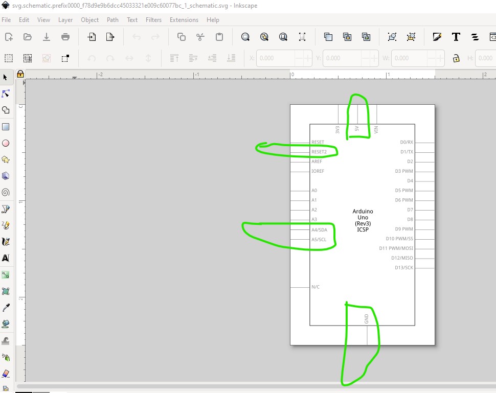
Even that is a problem. The ICSP pins for instance on the original UNO are overlaid on their standard pin positions. On the newer boards they are separate pins on the cpu (and in the case of the wifi boards, on a different processor!) and thus need to be separated and it isn’t clear to me how to do that. This is the core UNO ICSP schematic
The pins circled in green are where the ICSP connections are overlaid in schematic. On the newer boards the various (some of the new boards have multiple ICSP or JTAG pins) are usually on separate unique CPU pins and thus will need to be shown somewhere. It isn’t clear to me where they should appear or how. As noted I prefer to show the pins as they appear on the ICSP connector in schematic (including the power and ground pins as that makes the most sense to me.) To do this we would need to decide how to represent things like the ICSP and jtag connectors in schematic and I currently don’t know how to do that.
edit:
A reason not to do this now is that doing so commits us to having to obsolete the new boards (which are available now if not in core parts or the desired format but they are available (and as long as they aren’t in core, obsoleting doesn’t apply!) when the final changes come. That is going to be a fair amount of work that I would rather avoid.
Hi, did anyone adapt the .inx file and the .py file to just use raw pixels? That seems sooo much easier in my opinion. So imperial or decimal don’t play a role anymore and the svg works only with pixels anyway, so …
I don’t understand why all this converting is needed.
Fritzing is working in the real world, while it will deal with drawings in px, it guesses (sometimes incorrectly) at the DPI settings. Illustrator I think still uses 72DPI, Inkscape used to use 90DPI and currently uses 96DPI (which didn’t used to be a choice in Fritzing, I’m unsure if that has changed in 1.0.3.) If the guess is wrong the part will have the wrong scale and the various views will be incorrect. Dimensions in either in or mm are preferred as they are converted from the real world values to whatever DPI is currently in use and there is no guessing involved to go wrong.
The problem is that there is not really a standard anymore in PPI (DPI is for printers) My 4K(3240x2160 px) 15" screen for example has 259.6 PPI so conversion on my screen will have a different outcome compared to another screen e.g. a FHD (1920x1200px) on a 10 inch screen.
Since SVG code only uses pixels, this problem becomes obsolete, since it is the GPU which will convert to dinmensional correct and comparable units. (sometimes the GUI of the app takes over)
In Fritzing one can zoom in or out as required, but I have problems with parts which are created imperial (too big) when I want to connect e.g. a resistor to an ESP32, which was created pixel based (so too small). If everything was pixel based, it would always fit, whatever resolution one is using. No guessing neither, just zoom more or less.
on DPI Calculator / PPI Calculator (sven.de) you can see how many different sizes a pixel can have, so at this moment there is no way of telling how to convert.
Over and over again I have to open the svg file to reduce or enlarge, and make sure I don’t loose the properties of the pins…
So, I am changing this extension to just use pure pixels. But it there are a lot of obstacles…
The extension only generates schematic svgs which are best when dimensioned in inches since they are intended to be on 0.1in boundaries. The extension works fine (at least for me) as is. Printing is a whole different issue and is handled (usually correctly AFAIK) by the Fritizng printer drivers if you are printing the sketch.
That is not really accurate. SVG “CAN” use pixels for coordinates, but it can also use physical units like inches or millimeters. Frizting wants physical units, because it display multiple images (parts) on the same screen. It needs to scale them all to a consistent size, so that pins on one part are the same size on every other part. As noted, pixels can be different sizes depending on the display hardware. The physical world units don’t change. It is (partly) up to the os and graphics driver software to figure out the pixels per unit size to show things reasonably. With physical units in the svg, Fritzing does not have to ‘guess’ what the correct way to match other parts is. The pixel size could have been different on each environment that the parts were created on.