Updated files :
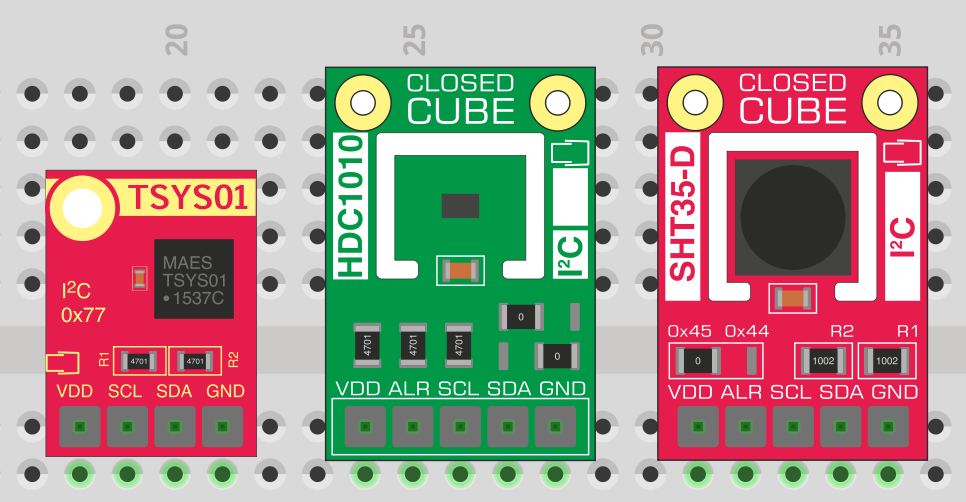
SHT35-D.fzpz
TSYS01.fzpz
HDC1010.fzpz
TSYS01.fzpz (23.3 KB)
Schematic view connection terminals not propperly defined:
They should have conection on the tip.
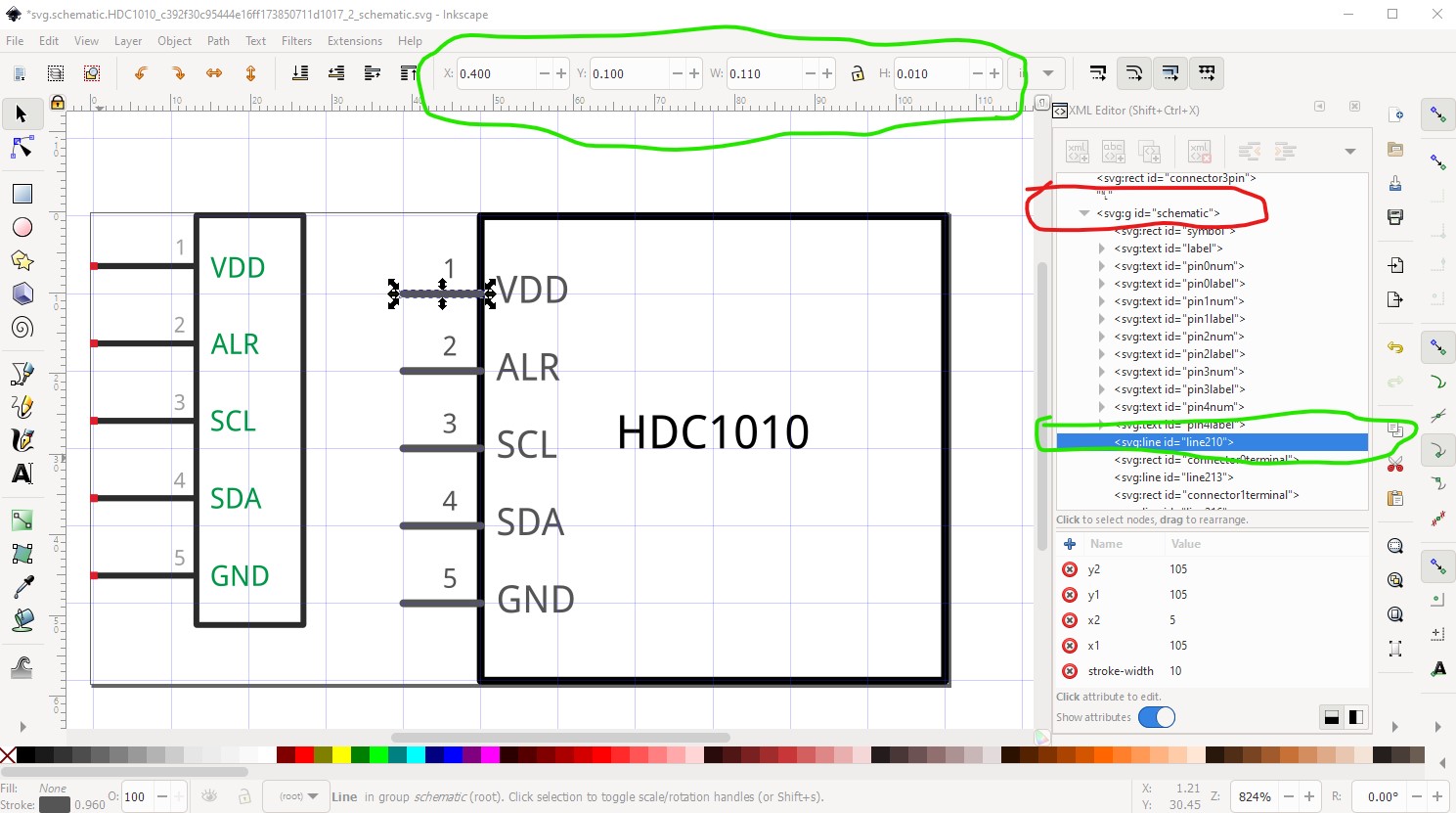
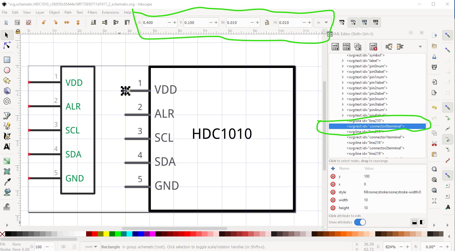
The problem is that you defined Width 0 in connection terminals
You should change from this:
to this:
to get this:
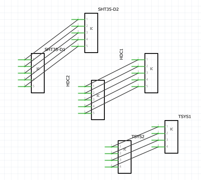
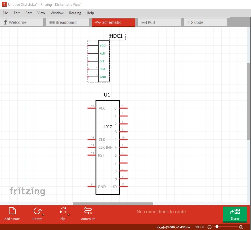
1234 1234 also makes no sense, we added the actual pin functions now
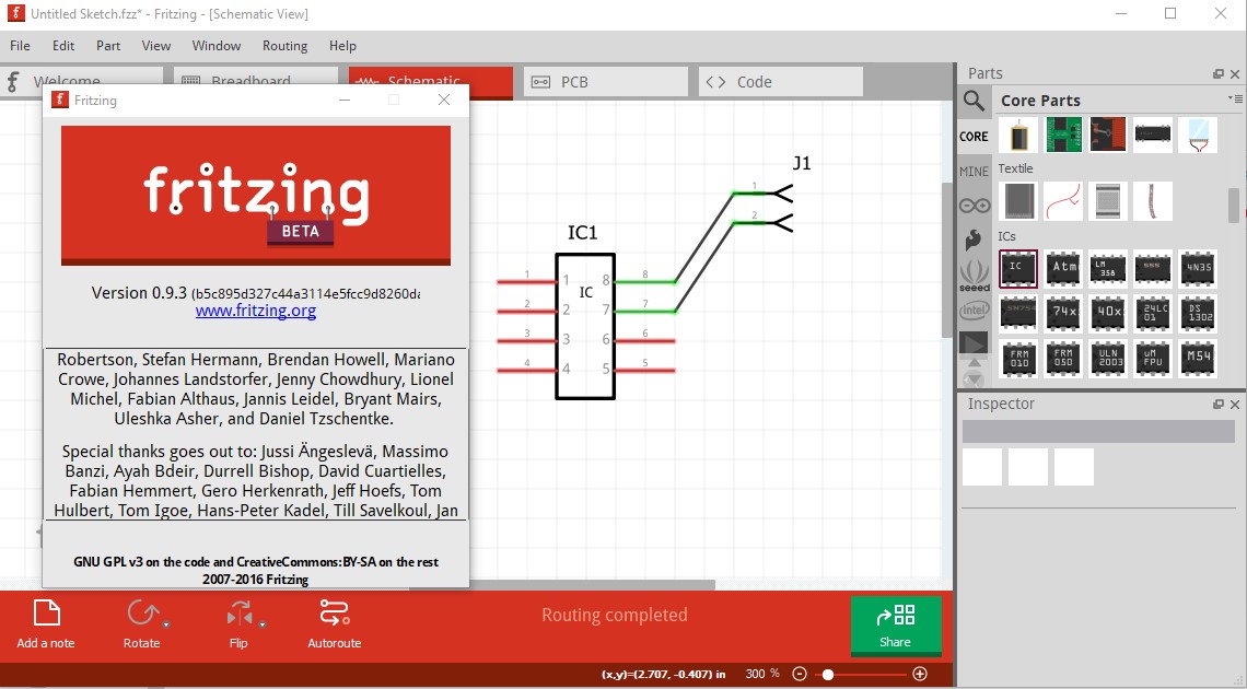
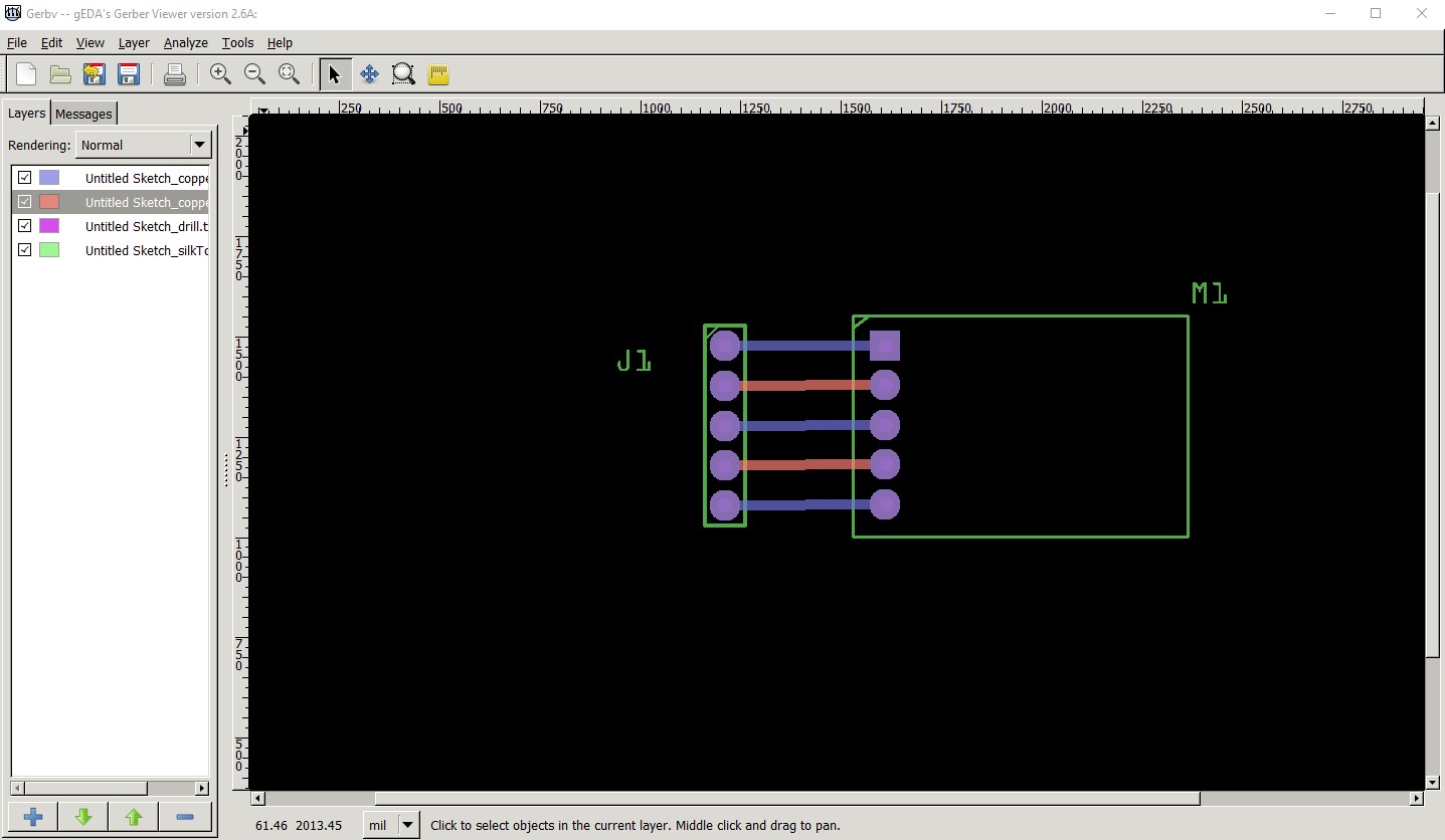
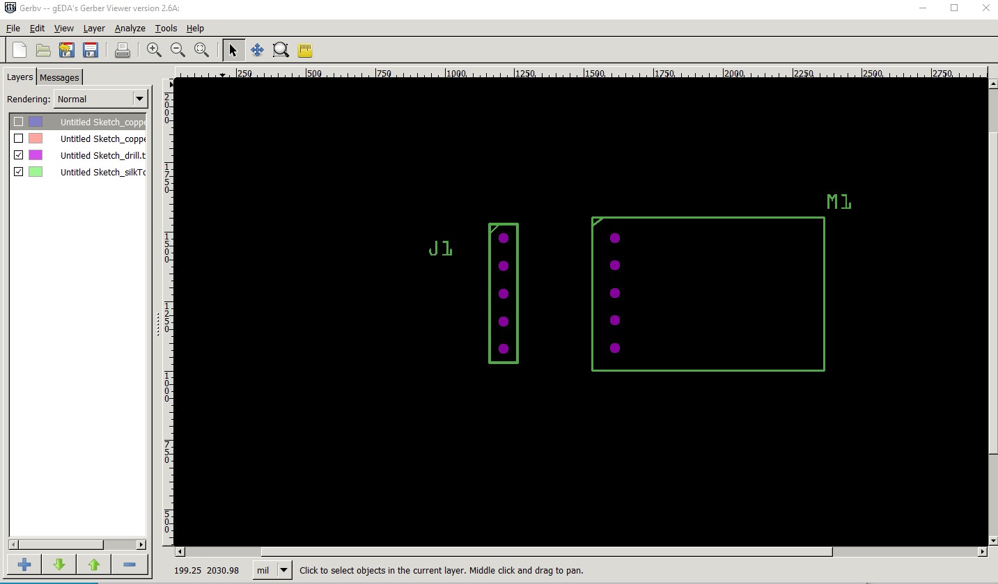
The terminalIds are actually a 0.9.6 bug. A zero width terminalId used to work (and parts factory generates them on the generic IC!) This is 0.9.3b with a generic IC dragged in to schematic and connected to a header. Aligned correctly.
this is 0.9.6 with the same input. TerminalId not recognized. I will report this as a bug.
As well at least the SHT35-D.fzpz (I didn’t check the others) has no breadboard layerId which will prevent the part from exporting as an image (png, jpg, pdf, svg)
Peter
Thank you for the update,
have you seen my updated version on top of this post ?
it should work on all versions of Fritzing
the ID’s of the connections are now present in the svg which is imported in the part editor and therefore present in the component library file.
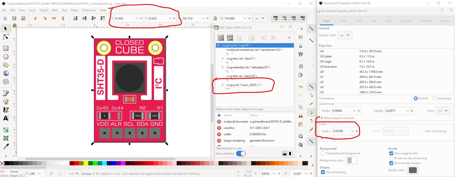
I have now. I fixed up the sht35-D part to meet the graphics standards like this (the others likely need the same) note I am using Inkscape here rather than Coraldraw so some things may be different for you. If you can figure out how to do the equivalent thing in Coraldraw the documentation would be appreciated to add to the tutorials section of the forum!
breadboard
slightly offset (not enough to matter likely) in starting coords
no layerId
incorrect scale
so ungroup rescale and regroup and name the group breadboard. Rescaling in Inkscape is described here:
don’t know how to do this in Coraldraw or Illustrator (not sure it is possible in Illustrator!) Which produces this:
which is pretty much identical except meets the standards which are available here:
part file format:
and the graphic standards
https://fritzing.org/fritzings-graphic-standards
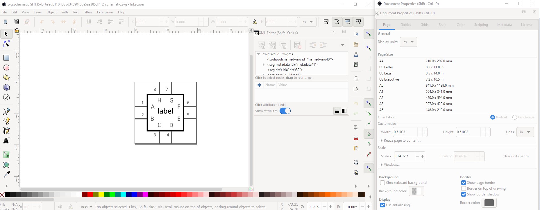
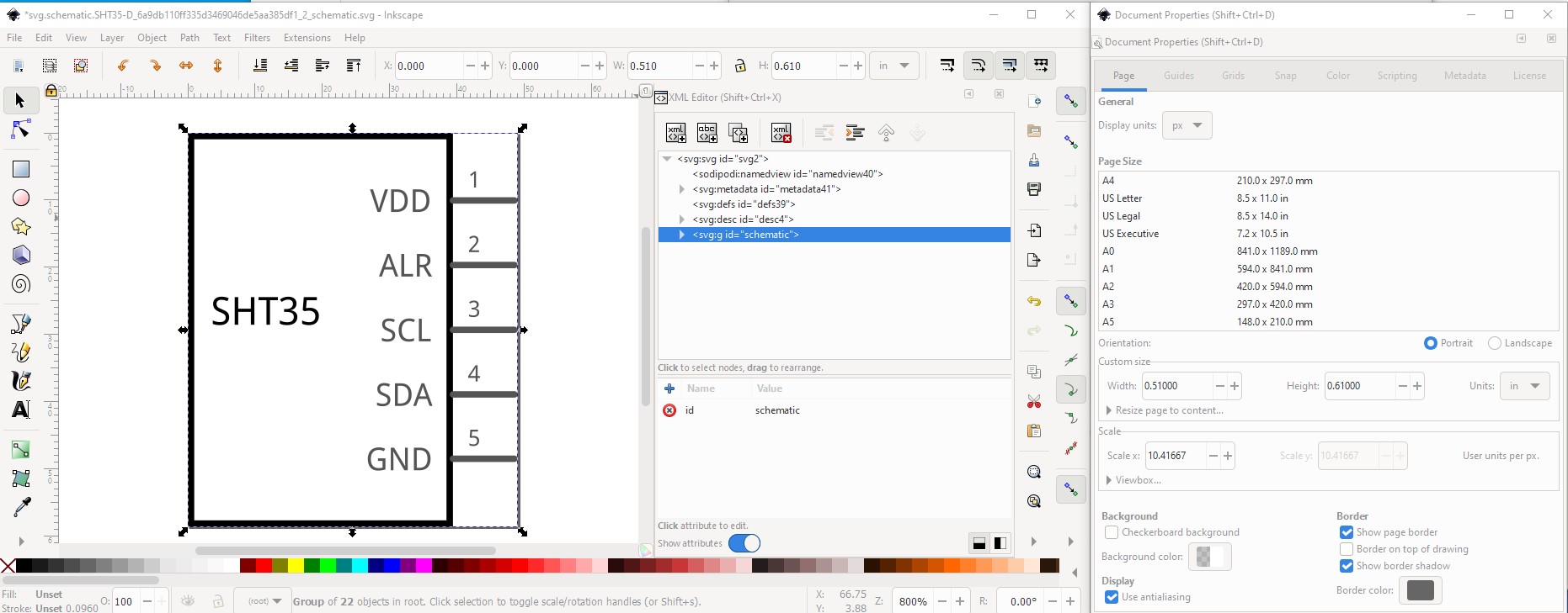
schematic
While this will work, it isn’t the correct scale and doesn’t meet the graphics standards and thus I chose to replace it with the template file which looks like this
which is available here:
Since this is a sensor and by convension in puts are on the left of schematic delete the left, top and bottom connectors then duplicate the other 3 connectors, add their labels and pin Ids to give the final schematic that meets graphic standard.
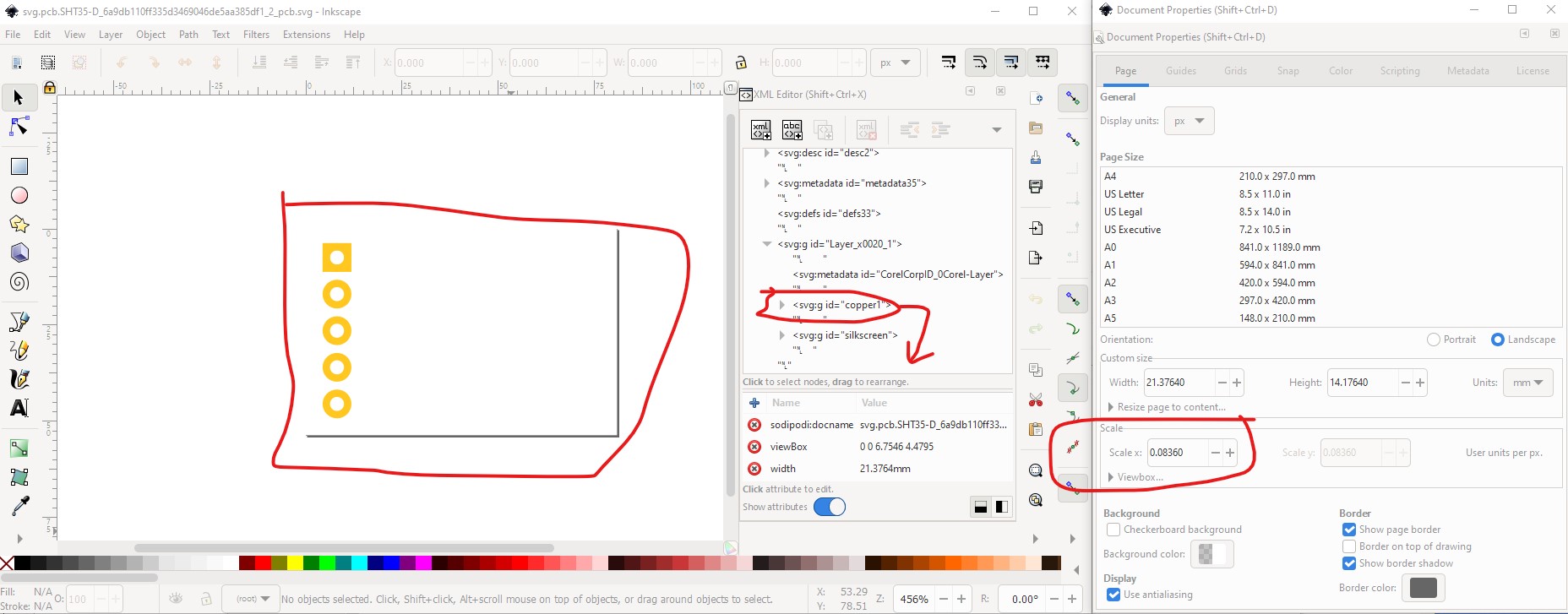
pcb
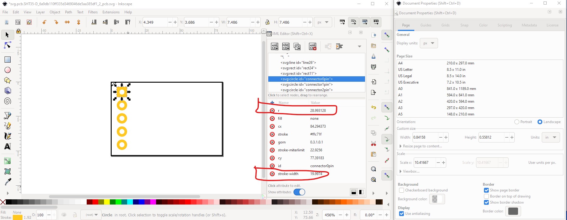
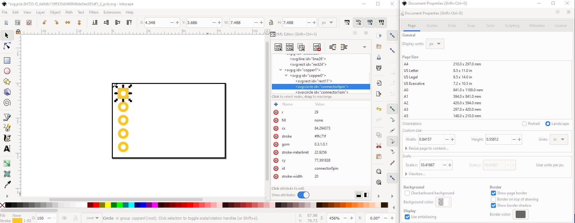
Incorrect scale, silkscreen color is white (old style) rather than black (current style) and copper layers are above silkscreen (which makes Fritzing select the silkscreen first which is undesirable.) So ungroup rescale and change silkscreen color from white to black. Then for each pin, set the radius to 29 and the stroke-width to 20 to produce a 0.038000 hole for a 0.1in header.
to produce the final pcb svg
fzp file (edited with a text editor rather than parts editor which I find mostly useless)
add a fritizng version number
<?xml version='1.0' encoding='UTF-8' standalone='no'?>
<module referenceFile="generic_sip_5_300mil.fzp" moduleId="SHT35-D_e71e8b6b9db09637b65141a2f76971d9_2" fritzingVersion="0.9.6">
Change the label to M (for module)
<title>SHT35-D</title>
<label>M</label>
add proper tags
<tag>SHT35-D</tag>
<tag>digital humidity sensor</tag>
<tag>sensor</tag>
<tag>fritzing user</tag>
change family to
<property name="family">SHT35-D</property>
<property name="variant">1</property>
as it is likely unique. The family should only be the same for parts that can be swapped for each other (although that is not true for all the parts in core, it should eventually be made to be that way.)
added a url pointing to the github code repository (which has pictures of the board so the user knows what they are looking to buy, I didn’t find many sales sites.)
<url>https://github.com/closedcube/ClosedCube_SHT31D_Arduino</url>
replaced the icon svg with the breadboard svg to save some file space.
ran the fzp file (and thus all the svgs) through FritzingCheckPart.py to fix up all the things Inkscape does which Fritzing does not support and to check for errors (such as missing layerIds)
$ FritzingCheckPart.py part.SHT35-D_e71e8b6b9db09637b65141a2f76971d9_2.fzp
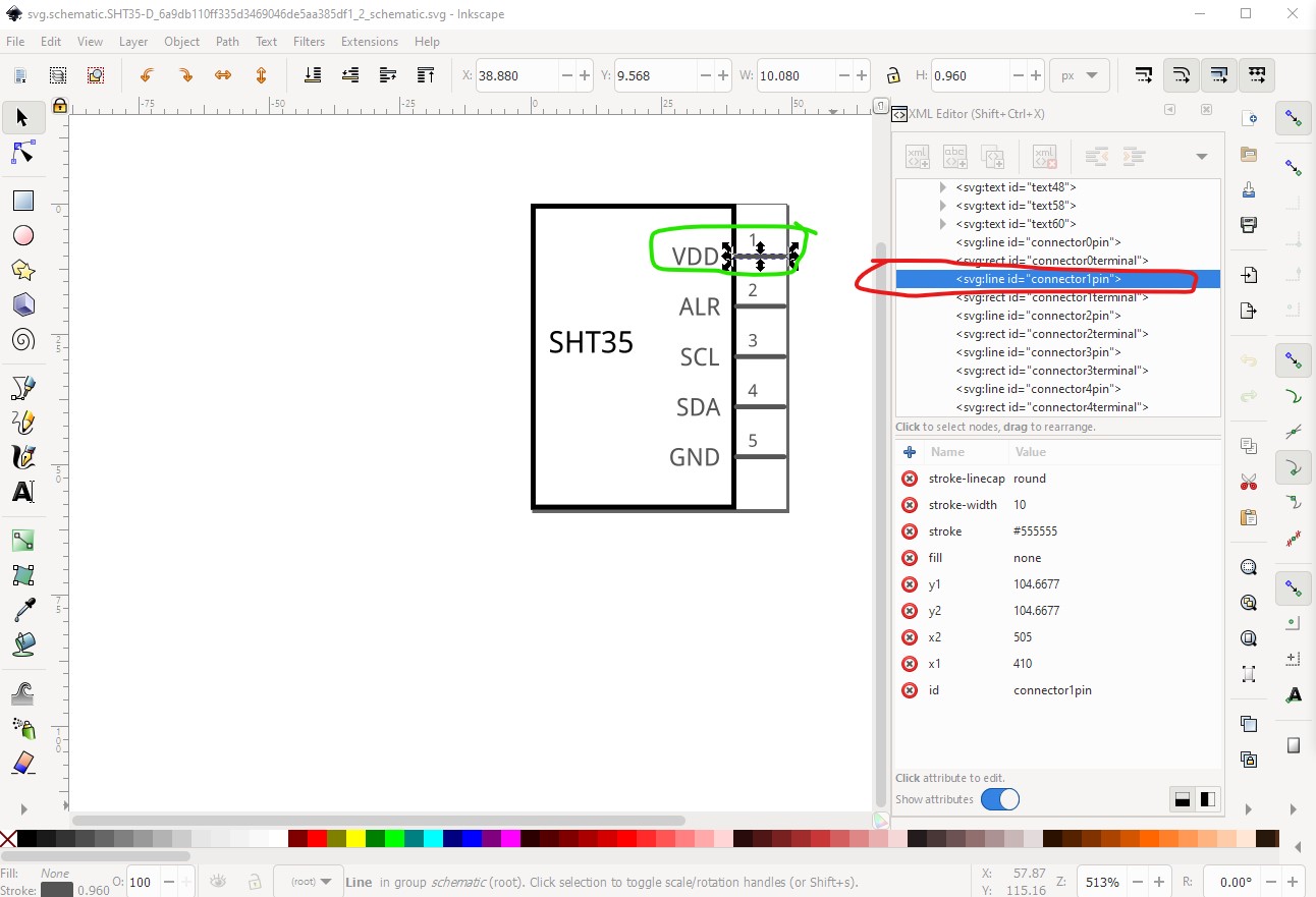
Use 7zip to zip the resulting files in to an fzpz file then load the result in to Fritzing for testing. That immediately shows up an error, in schematic I reversed pins 1 and 2 (connector0 and 1):
so go back and correct that!
It now looks correct
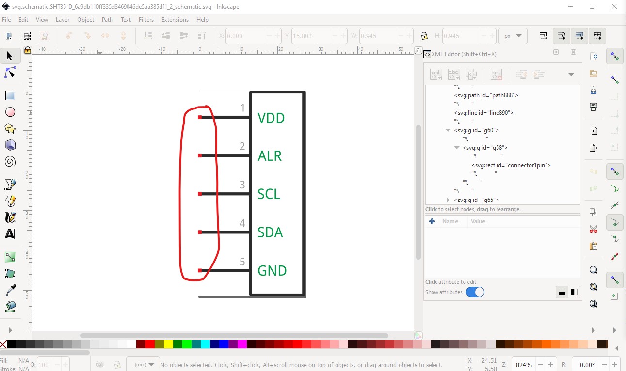
note the entire .1in of the pin is green (or red if it is not connected) here and the terminalId insures the wire connects to the end of the pin.
run DRC (Routing->Design Rules Check) to verify it is OK.
move a couple of traces to the top layer to make sure traces on both sides work (this won’t find all possible errors but covers most of them!) Then export the pcb as gerber files and check the gerber output is correct. Firt edit the drill.txt file with a text editor and verify the holes are all 0.038in:
; NON-PLATED HOLES START AT T1
; THROUGH (PLATED) HOLES START AT T100
M48
INCH
T100C0.038000
%
T100
X016111Y010817
X016111Y014777
the 0.038000 in T100C0.038000 indicates the hole size in inches.
then view the board in a gerber viewer to make sure the translation took place correctly (this occurs after pcb view in Fritzing so problems that won’t show up in Fritzing are possible here.)
then suppress copper layers to leave only the drill holes to make sure all holes expected have been drilled.
which results in this corrected part (which has the same moduleId and files as the original, so you will need to delete that part before being able to load this one!)
SHT35-D-improved.fzpz (17.6 KB)
hope this helps!
Peter
A question for vanepp regarding graphic standards.
BTW thaks for it as I didn’t know that they existed.
I dowloaded the template file and found something in SVGs. What are these empty layers inside pcb SVG for? :
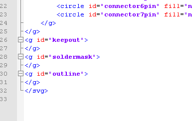
Should I guess you can customize part cutouts and soldermask?
I think future growth. I’m not aware of any way to use them although there may be.
Peter
Can somebody please check my updates and confirm they are ok ?
Sure if you upload the .fzpz files here (upload is 7th icon from the left in the reply menu!)
Peter
HDC1010.fzp (4.6 KB)
SHT35-D.fzp (4.7 KB)
TSYS01.fzp (4.1 KB)
HDC1010.fzpz (24.6 KB)
SHT35-D.fzpz (27.4 KB)
TSYS01.fzpz (23.3 KB)
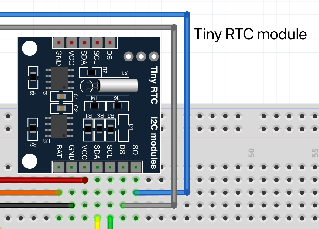
Can you also check another part i have manually made ?
RTC Time Module.fzpz (51.5 KB)
Over all a nice job, but a few problems. All the parts are pretty much the same so I’ll use the HDC1010 as an example. First I ran the part through FritzingCheckPart.py (available here)
which produces these errors:
Error 69: File
‘svg.breadboard.HDC1010_c392f30c95444e16ff173850711d1017_2_breadboard.svg.bak’
At line 17
Found a drawing element before a layerId (or no layerId)
Error 69: File
‘svg.schematic.HDC1010_c392f30c95444e16ff173850711d1017_2_schematic.svg.bak’
At line 17
Found a drawing element before a layerId (or no layerId)
Error 18: File
‘part.HDC1010_15573dc279dec0c8441631364ba10f98_1.fzp.bak’
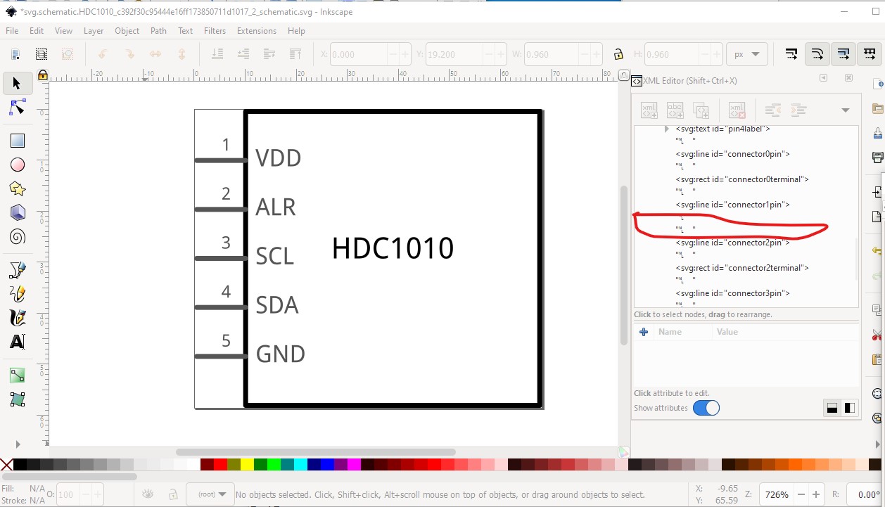
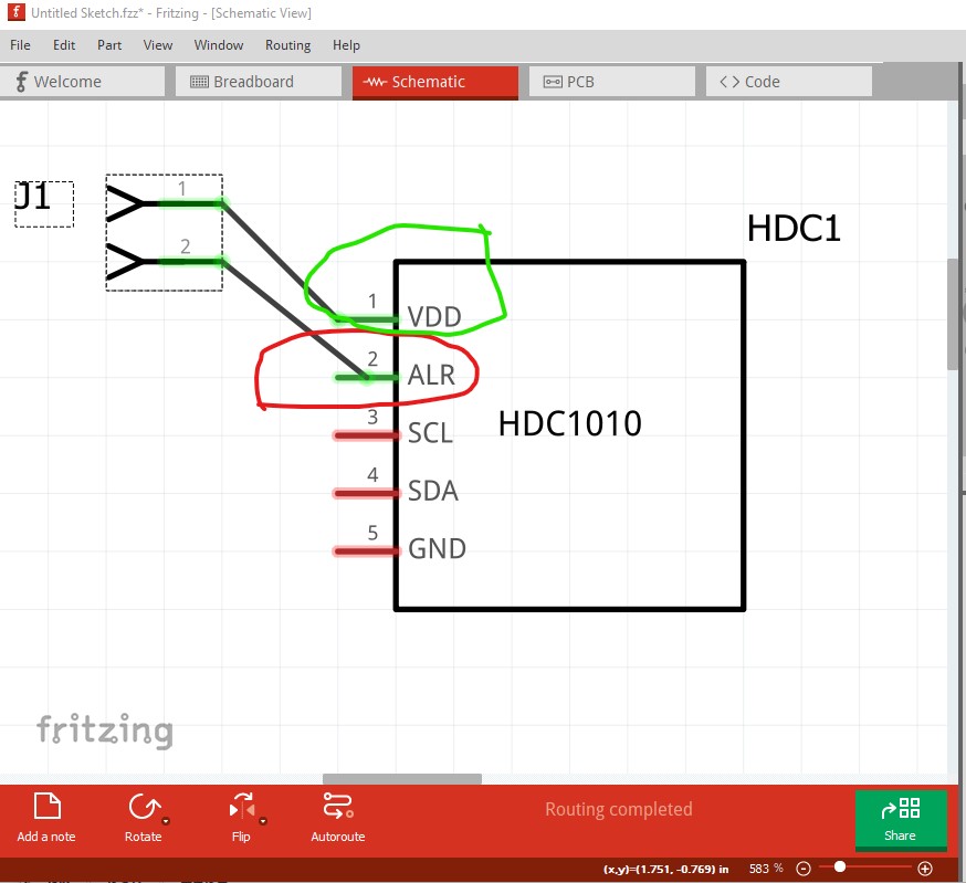
Connector connector0terminal is in the fzp file but not the svg file. (typo?)
svg svg.schematic.HDC1010_c392f30c95444e16ff173850711d1017_2_schematic.svg.bak
Error 18: File
‘part.HDC1010_15573dc279dec0c8441631364ba10f98_1.fzp.bak’
Connector connector1terminal is in the fzp file but not the svg file. (typo?)
svg svg.schematic.HDC1010_c392f30c95444e16ff173850711d1017_2_schematic.svg.bak
Error 18: File
‘part.HDC1010_15573dc279dec0c8441631364ba10f98_1.fzp.bak’
Connector connector2terminal is in the fzp file but not the svg file. (typo?)
svg svg.schematic.HDC1010_c392f30c95444e16ff173850711d1017_2_schematic.svg.bak
Error 18: File
‘part.HDC1010_15573dc279dec0c8441631364ba10f98_1.fzp.bak’
Connector connector3terminal is in the fzp file but not the svg file. (typo?)
svg svg.schematic.HDC1010_c392f30c95444e16ff173850711d1017_2_schematic.svg.bak
Error 18: File
‘part.HDC1010_15573dc279dec0c8441631364ba10f98_1.fzp.bak’
Connector connector4terminal is in the fzp file but not the svg file. (typo?)
svg svg.schematic.HDC1010_c392f30c95444e16ff173850711d1017_2_schematic.svg.bak
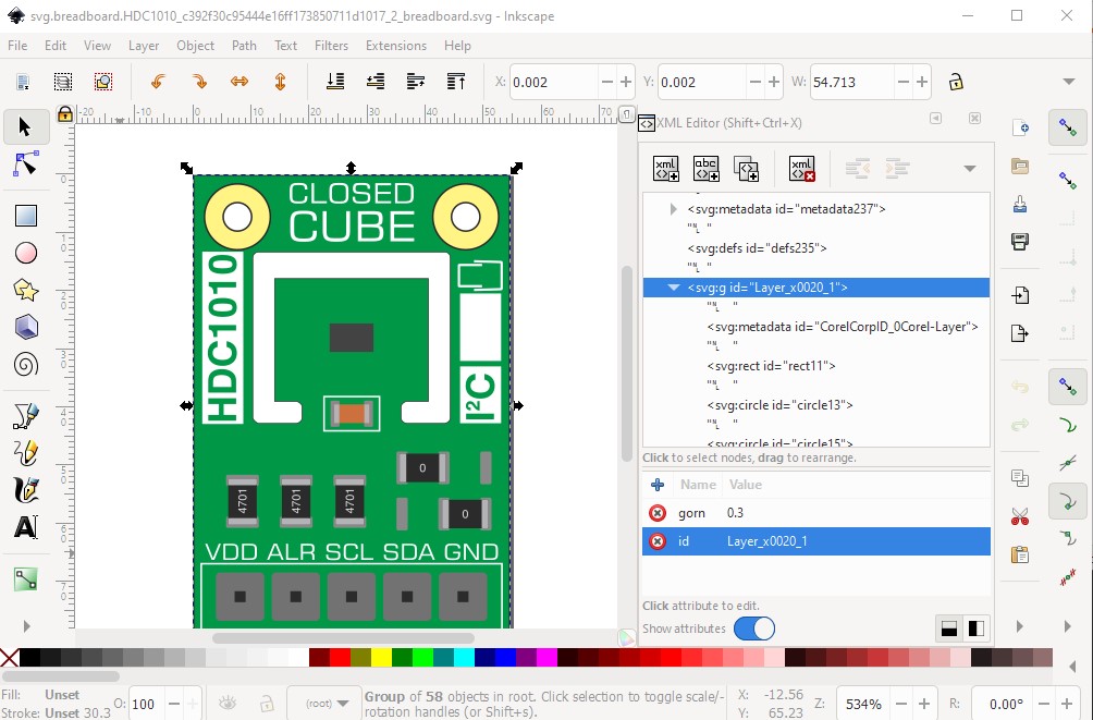
The layerId is missing in both breadboard and schematic. The effect of that is the part won’t export as an image (svg, png, jpg etc.) the wires to the part will appear but the part itself will be blank. The easiest way to fix that is to rename group Layer_x0020_1 here to breadboard
the layerId needs to match the value in the .fzp file in this case breadboard, found here in file part.HDC1010_15573dc279dec0c8441631364ba10f98_1.fzp
<breadboardView>
  <layers image="breadboard/HDC1010_c392f30c95444e16ff173850711d1017_2_breadboard.svg">
    <layer layerId="breadboard"/>
  </layers>
</breadboardView>
Schematic:
In the schematic case the layerId needs to be schematic. As well, while the current schematic will work, it is preferable to have one that conforms to the graphics standard available here:
https://fritzing.org/fritzings-graphic-standards
It is preferable (so all the parts match in schematic) that parts look like this (this was generated by the Inkscape Fritzing-Schematic extension and meets the graphics standards.)
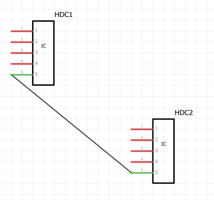
Here the pin is .110in long and has a .01in by .01in terminalId on the end of the pin. The effect of this in Fritznig is this:
The top is your current part, under it is a par t from core in the standard format. Note the pin is .1in (actually probably 0.105in or 0.11in) long and is colored red by Fritzing. The longer pin makes connections to it easier. The terminalId is on the left end of the pin (and if it is missing, the connection will be to the center of the pin which is incorrect!) Here I intentionally deleted the connector1terminal element to demonstrate what happens when the terminalId is missing.
In Fritzing that produces this:
Here pin1 has a correctly positioned terminalId so the wire terminates as it should at the end of the wire. Pin2 however is missing its terminalId and the wire terminates in the middle of the pin (which is incorrect!) As well it is desirable to set the label value in the fzp file to M (for module) rather than HDC1010 (which as we see in the image above gets truncated to HDC to form label HDC1. So replace
<label>HDC1010</label>
in the fzp file with
<label>M</label>
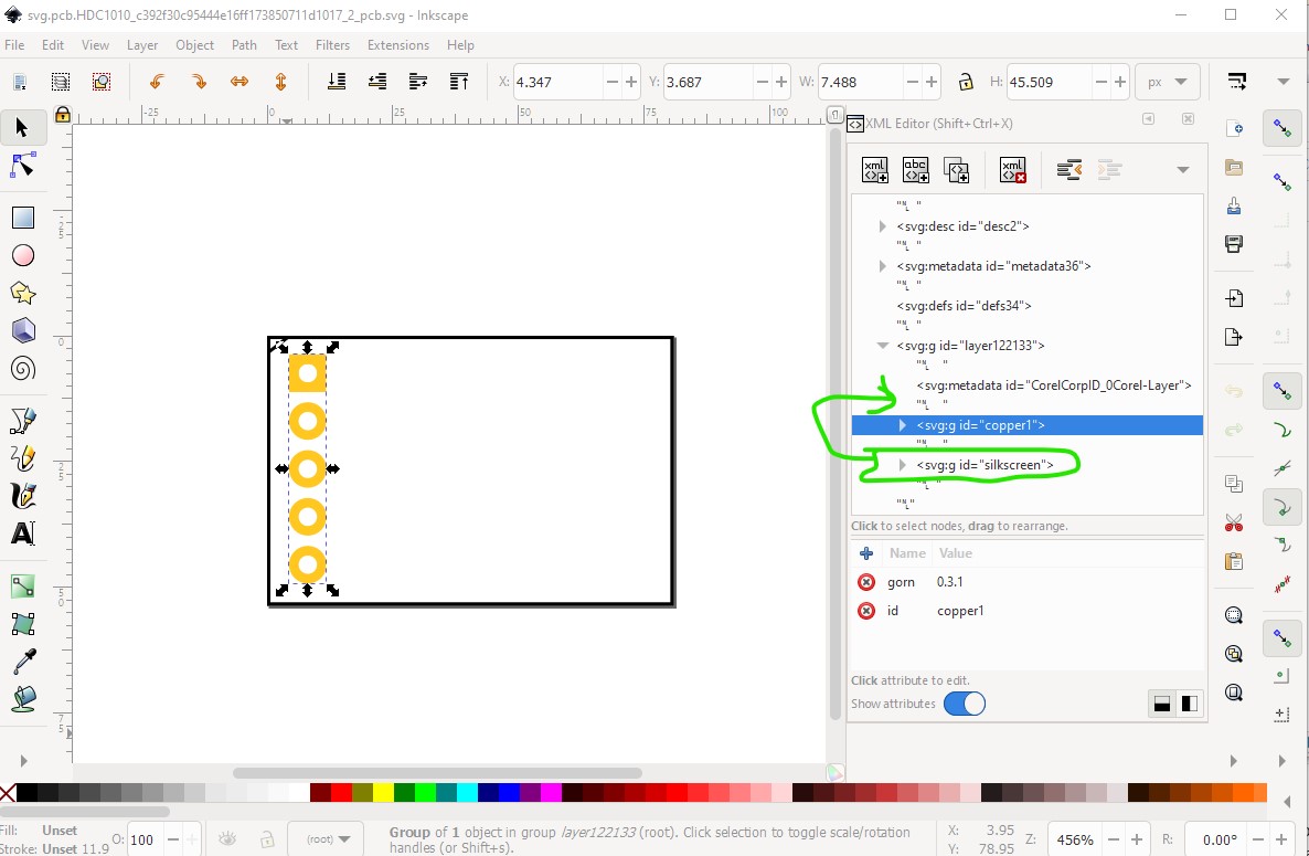
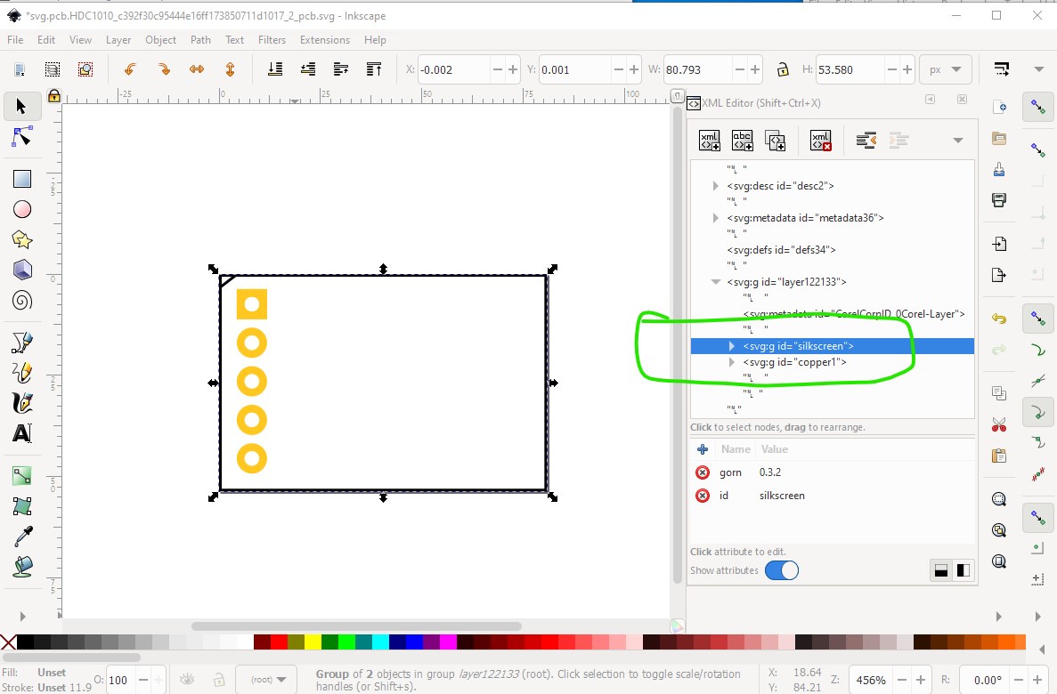
to make that change. It is also desirable to move the silkscreen group in the pcb svg to be above the two copper groups like this:
to look like this:
FritzingCheckPart produces this warning about the layerIds:
Warning 25: File
‘svg.pcb.HDC1010_c392f30c95444e16ff173850711d1017_2_pcb.svg.bak’
At line 123
Silkscreen layer should be above the copper layers for easier selection
in pcb view
(a warning because it doesn’t stop Fritzing from working, it just makes silkscreen select first over the copper layers which is usually not what you want!)
Peter
Thanks for checking.
however, i use these fritzing models succesfully, make gerber files and have PCB’s made so is all this work necessary ?
Sounds like a lot of work.
Is there no easier way to create models ?
Is there a standard manual how to create flawless models ?
I see so much errors,
if it is clear how to solve them quick, i would be prepared to do the effort, oterwise i will keep producing models with errors since they work in practice
Can you please check the last model ?
A couple of errors should be solved
$ python3 FritzingCheckPart.py
Traceback (most recent call last):
File “FritzingCheckPart.py”, line 52, in
import FritzingTools as Fritzing, PPTools as PP
File “/Users/Maurice/Documents/FritzingCheckPart-master/FritzingTools.py”, line 29, in
import os, sys, re, logging, PPTools as PP
File “/Users/Maurice/Documents/FritzingCheckPart-master/PPTools.py”, line 26, in
from lxml import etree
ModuleNotFoundError: No module named ‘lxml’
MauricesMBP700:FritzingCheckPart-master Maurice$ chmod 777 *.py
MauricesMBP700:FritzingCheckPart-master Maurice$ python3 FritzingCheckPart.py
Traceback (most recent call last):
File “FritzingCheckPart.py”, line 52, in
import FritzingTools as Fritzing, PPTools as PP
File “/Users/Maurice/Documents/FritzingCheckPart-master/FritzingTools.py”, line 29, in
import os, sys, re, logging, PPTools as PP
File “/Users/Maurice/Documents/FritzingCheckPart-master/PPTools.py”, line 26, in
from lxml import etree
ModuleNotFoundError: No module named ‘lxml’