I have drawn the part on a 0.1 grid in Inkscape as an svg, but the instructions to turn it into an fzp part are frying my brain. Can anyone help me turn into a fritzing part please?
I dropped the part on pastbin.
I have drawn the part on a 0.1 grid in Inkscape as an svg, but the instructions to turn it into an fzp part are frying my brain. Can anyone help me turn into a fritzing part please?
I dropped the part on pastbin.
Your svg lacks connectors. First item of business however is which one you want. I would guess it is the wireless-tag version, but does this look like the board you have?
Peter
Yes that is the one.
After some more looking at docs and vids, I see that I should have broken up the connectors rather than have them combined.
Am I correct that I break it down into separate connectors for the breadboard, then draw again for the pcb, I can just use fritzings new part editor? The guides I tried to follow had me editting svg files with a text editor, but seen some videos that show it being done inside firtzing. That looks more straightforward.
Not entirely. You need an existing fzp file with the correct number of pins defined before parts editor will work correctly. As to tutorials, these two sets apply to the current versions of Fritzing many of the others are pre parts editor (note I rarely use parts editor and thus didn’t cover it, Old_Grey does cover parts editor.) Assuming you use Inkscape, Randy’s schematic creation extension makes creating schematic easy.
schematic Inkscape plugin
Or I can create a part if you like.
Peter
I’d be very grateful if you would create it.
But I am also keen to figure out how to do it myself. I’ll follow the links provided and see how things go.
Thanks for the help.
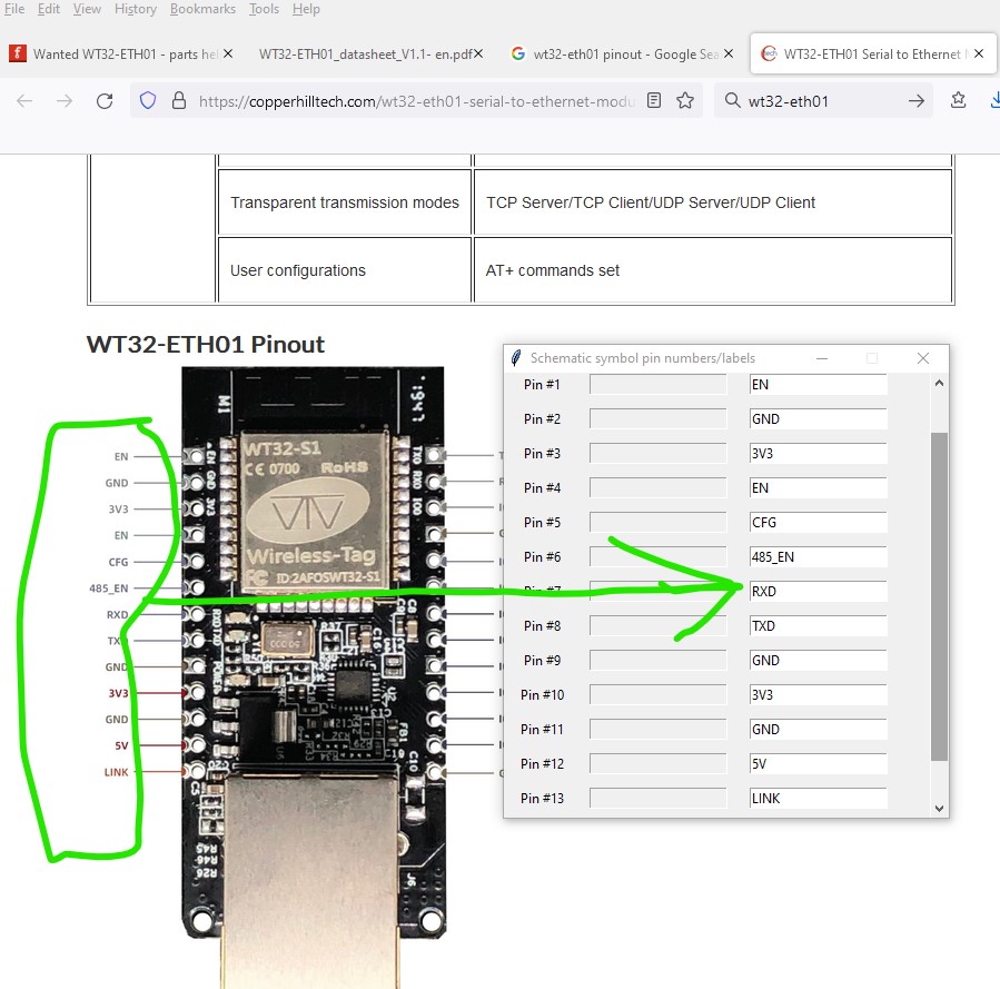
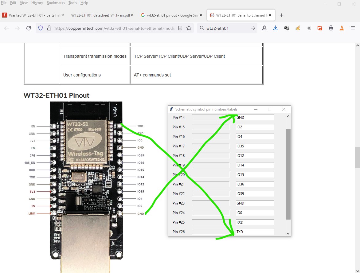
OK this should do what you want with a few potential issues. The documentation isn’t very good, they reused pin numbers in the official pdf and what pins connect together internally isn’t clear.
wt32-eth01.fzpz (21.1 KB)
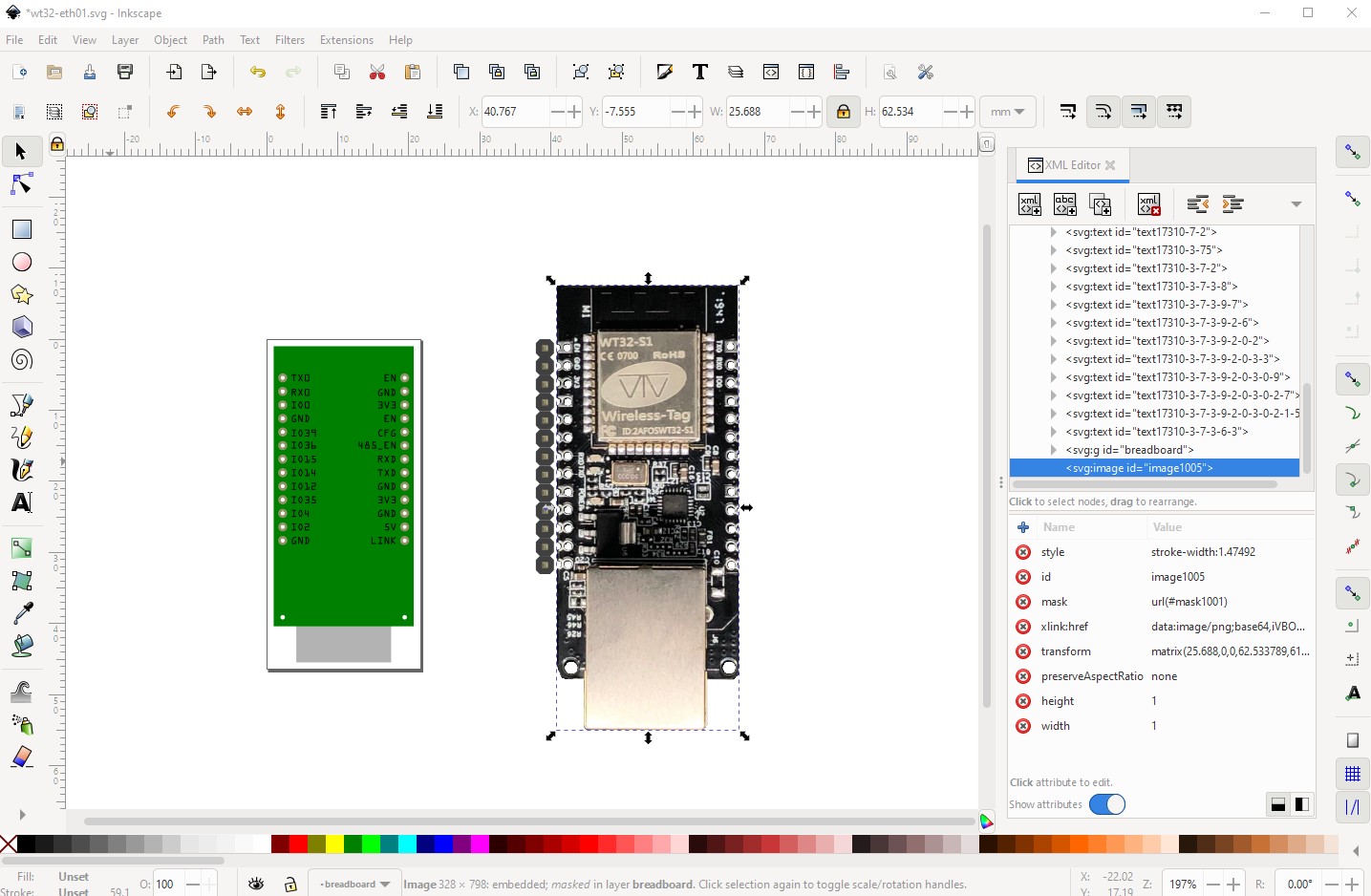
Here is a fairly brief explanation of how I made this. For breadboard I started from scratch and in Inkscape imported page 8 of the data sheet from Seeed above as the dimensions don’t seem to be documented that I can find easily.
I resized the image to match a 13 pin male header beside it and then used the image to create breadboard ending up with this:
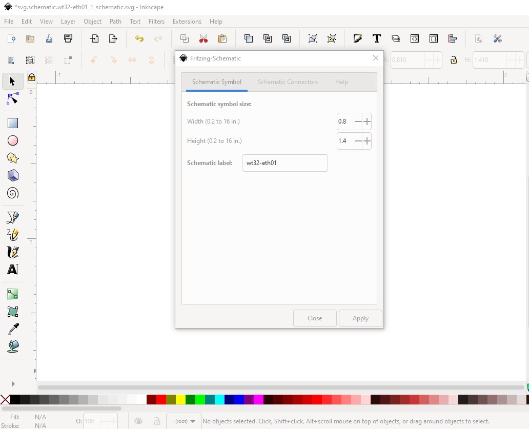
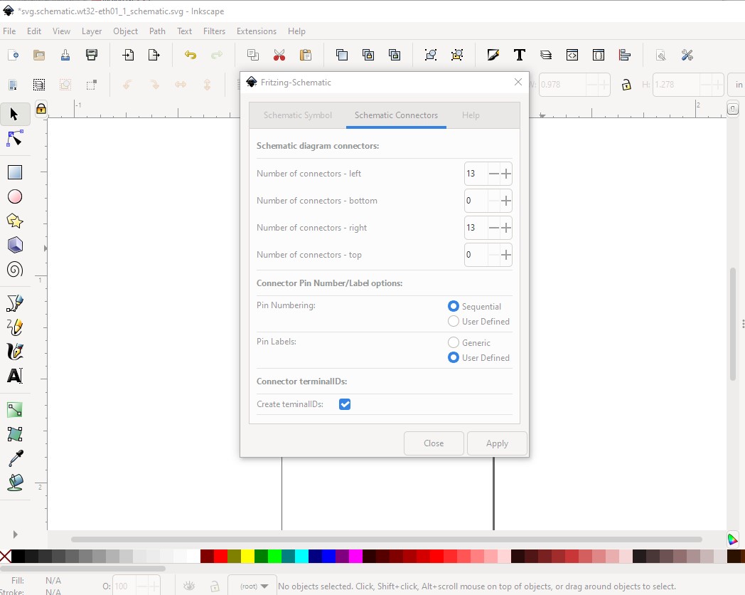
Then I used the schematic extension to make schematic.
The pin names were taken from
as they are easier to understand than those in the pdf ( I eventually realized the pdf is right, just confusing as they reused pin numbers from the programming interface!)
Note the schematic extension starts the right side pins at the bottom!
hitting finish when done creates the schematic svg (which meets the graphics standards!)
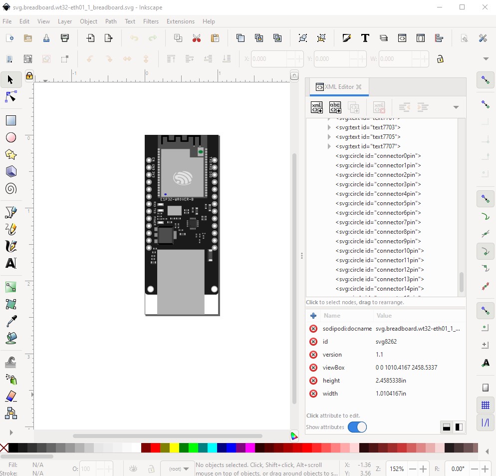
For pcb I copied the breadboard svg and modified it to be suitable for pcb. Of note is the mounting holes are only in silkscreen, they will not be drilled by default. The reason is that you can drag a hole from core parts/pcb in to the sketch to drill the mounting holes, but if you don’t want mounting holes and they are in the part, then you need to modify the part to delete them. Then I created a .fzp file and copied the pin descriptions from the data sheet in to them, added the needed buses (I am assuming the two enable pins, the grounds and the 2 3.3V pins connect internally on the board) then ran the whole part through FritzingCheckPart.py to make sure it appears correct (and clean up some Inkscapeisms!) The result is the .fzpz file above.
Peter
Just, Wow!
I never expected it to be so detailed or that you would do it so quickly. I am really very, very grateful.
Likewise, I should have said about the reused pin numbers. I tripped over it and was at a loss for a while. Top 6 pins debugging/flashing, remainder restart at pin 1 for general and io. What a strange thing to do.
As I learn more, I hope to repay your efforts doing something similar for others.
Thank you once more.