this is a continuation of the family and variant howto here:
This howto details the various ways to suppress the pcb layer in a part. As with the earlier parts of this series I will use the yahboom super-bit part as the example. Because there is a 18650 battery (and a BBC micro:bit plugged in vertically to a socket on the super:bit) it isn’t practical to place a pcb on top of the super:bit. Rather than do the work (there are 86 connectors!) required to make pcb view work, I chose to suppress pcb view instead. The official way to suppress pcb view (as explained in the parts files format document available here:
is to use the Hybrid Connectors property (described in a section called Hybrid connectors (optional) near the bottom of the document. Below is an example of where this is useful using a barrel adapter part that has screw terminals (the other common case to want to suppress pcb view):

here we have a 2.1 barrel adapter to screw terminal adapter. Actually neither of these translate well to pcb, but the screw terminal part is an example that often wants to be suppressed in pcb, so that is what we will do here. There are at least two ways to do that, by setting hybrid=“yes” in the fzp file (which in this case runs in to a Fritzing bug) and eliminating the pcbview section of the screw terminal connectors in the fzp file (which is what I actually did in the published part.) Lets start with the variant 2 part which uses hybrid=“yes”. This is in this Fritzing part:
2.1mm Barrel Jack with Terminal Block-improved-hybrid.fzpz (6.4 KB)
and the relevant section of the fzp file looks like this:
<connectors>
  <connector id="connector0" type="male" name="POS-TERM">
    <description>positive connector terminal block</description>
    <views>
      <breadboardView>
        <p layer="breadboard" svgId="connector0pin"/>
      </breadboardView>
      <schematicView>
        <p layer="schematic" svgId="connector0pin" terminalId="connector0terminal"/>
      </schematicView>
      <pcbView>
        <p layer="copper1" svgId="connector0pin" hybrid="yes"/>
        <p layer="copper0" svgId="connector0pin" hybrid="yes"/>
      </pcbView>
    </views>
  </connector>
 ... (connector 1 is indentical except for connecotr number and name/description)
  <connector id="connector2" type="male" name="POS-Barrel">
    <description>positive barrel connector</description>
    <views>
      <breadboardView>
        <p layer="breadboard" svgId="connector2pin"/>
      </breadboardView>
      <schematicView>
        <p layer="schematic" svgId="connector2pin" terminalId="connector2terminal"/>
      </schematicView>
      <pcbView>
        <p layer="copper1" svgId="connector2pin"/>
        <p layer="copper0" svgId="connector2pin"/>
      </pcbView>
    </views>
  </connector>
 ... (again connector3 is identical to 2 except for connector number and name/description)
<buses>
  <bus id="pos">
    <nodeMember connectorId="connector0"/>
    <nodeMember connectorId="connector2"/>
  </bus>
  <bus id="neg">
    <nodeMember connectorId="connector1"/>
    <nodeMember connectorId="connector3"/>
  </bus>
</buses>
Connector0 is bused to Connector2
Connector1 is bused to Connector3
The alternate part in
2.1mm Barrel Jack with Terminal Block-improved.fzpz (6.3 KB)
(which has a different module id and variant and so will load alongside the first version) is identical except that instead of hybrid=“yes”, the pcbview section of connectors 0 and 1 look like this:
<connectors>
  <connector id="connector0" type="male" name="POS">
    <description>positive connector barrel jack </description>
    <views>
      <breadboardView>
        <p layer="breadboard" svgId="connector0pin"/>
      </breadboardView>
      <schematicView>
        <p layer="schematic" svgId="connector0pin" terminalId="connector0terminal"/>
      </schematicView>
    </views>
  </connector>
This does not use the hybrid=“yes” construct but rather deletes the pcbview sections of the connectors to be suppressed. The effect is mostly identical, as we see in this pcb view image, the two parts look identical, the pcb view of connectors 0 and 1 are not present in pcb. The difference is when in pcb view you hover over the pins so the labels come up, in the hybrid case those labels are incorrect (which is likely a Fritzing bug):
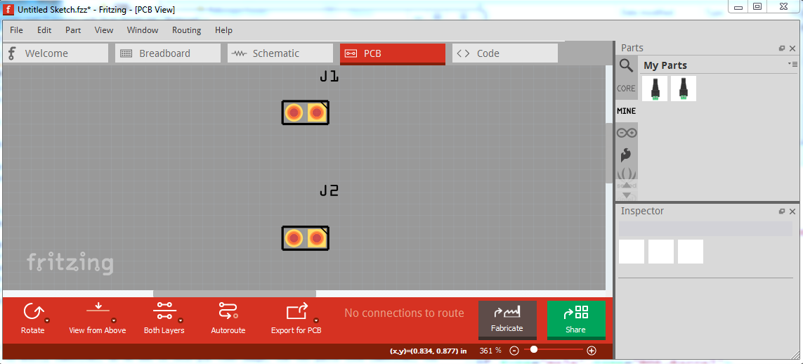
this problem I haven’t been able to capture as a image, because it will only happen when you hover over the pins in pcb view (which stops when I exit to take the screen capture) so to see this you will need to load the two parts in to Fritzing and try it. If you hover over the left most pin of J1 (the non hybrid variant 1 part) you will get the message:
NEG-Barrel: negative
barrel connector (4)
2.1mm Barrel jack with
terminal block
as expected.
the right pin gives
POS-Barrel: positive
barrel connector (3)
2.1mm Barrel jack with
terminal block
again as expected. The problem is with the hybrid=“yes” part J2 where the hovering over the left connector gets:
NEG-TERN:negative
connector terminal block
(2)
2.1mm Barrel jack with
terminal block
which is wrong, this is the barrel jack connection pin 4 not the terminal block pin 2. The right pin gives:
NEG-TERN:negative
connector terminal block
(2)
2.1mm Barrel jack with
terminal block
which is also wrong as it is the positive barrel jack pin 3. As a result I prefer to use the delete the pcbview option to suppress individual pins in pcbview. Now let us look at eliminating pcbview completely. First lets look at why you may want to do this. For example in this part (the roborio in core parts):
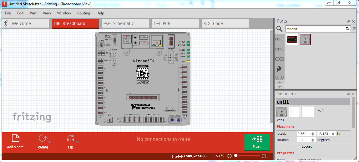
pcbview makes no sense. You could not mount a pcb on this part, it won’t fit, so here I supressed (incorrectly at present!) the entire pcb view
the problem with this as it stands is if you edit it and made it in to a standalone part, it would not export in the temp parts bin as a .fzpz file in the .fzz file of the sketch, because the pcb view suppression is incorrect. I created this part from this:
    <layers image="schematic/roborio_1_schematic.svg">
      <layer layerId="schematic"/>
    </layers>
  </schematicView>
  <pcbView>
    <layers image="pcb/roborio_1_pcb.svg">
      <layer layerId="silkscreen"/>
      <layer layerId="copper0"/>
      <layer layerId="copper1"/>
    </layers>
  </pcbView>
</views>
<connectors>
to this (which is incorrect):
    <layers image="schematic/roborio_1_schematic.svg">
      <layer layerId="schematic"/>
    </layers>
  </schematicView>
</views>
<connectors>
This appears to work, the part as a .fzpz file works fine, pcbview is suppressed. The problem is that when you include the part in a sketch and save the resulting sketch as a .fzz file, this part will not be included in the temp parts bin and the .fzz file will complain that it can’t find this part and the sketch will be incomplete. As noted in the parts file format, the format that works is to reuse breadboard view as pcbview like this using as an example the correctly configured part here:
super-bit.fzpz (51.6 KB)
instead of eliminating the pcbview section, here it has been replaced by a pointer to the breadboard layerId which leaves Fritzing with a “pcbview” that it is happy with:
  <views>
    <iconView>
      <layers image="breadboard/super-bit_1_breadboard.svg">
        <layer layerId="icon"/>
      </layers>
   </iconView>
  <breadboardView>
    <layers image="breadboard/super-bit_1_breadboard.svg">
      <layer layerId="breadboard"/>
    </layers>
  </breadboardView>
 <schematicView>
    <layers image="schematic/super-bit_1_schematic.svg">
      <layer layerId="schematic"/>
    </layers>
  </schematicView>
  <pcbView>
    <layers image="breadboard/super-bit_1_breadboard.svg">
      <layer layerId="breadboard"/>
    </layers>
  </pcbView>
</views>
This is how the super-bit part above is configured. In addition to the above change, you also need to remove the pcbview section from all the connectors. As an example here is the normal connector0 definition for this part:
<connectors>
  <connector id="connector0" type="male" name="P13">
    <description>P13 / SPI1 SCK port on the Micro:bit</description>
    <views>
      <breadboardView>
        <p svgId="connector0pin" layer="breadboard"/>
      </breadboardView>
      <schematicView>
        <p svgId="connector0pin" layer="schematic" terminalId="connector0terminal"/>
      </schematicView>
      <pcbView>
        <p layer="copper0" svgId="connector0pin"/>
        <p layer="copper1" svgId="connector0pin"/>
      </pcbView>
    </views>
  </connector>
In this case we want to delete the pcbview section as it is not used and will cause Fritzing to try and find the non existent connectors in pcb view and wastes disk space if left in, to have:
<connectors>
  <connector id="connector0" type="male" name="P13">
   <description>P13 / SPI1 SCK port on the Micro:bit</description>
    <views>
      <breadboardView>
        <p svgId="connector0pin" layer="breadboard"/>
      </breadboardView>
      <schematicView>
        <p svgId="connector0pin" layer="schematic" terminalId="connector0terminal"/>
      </schematicView>
    </views>
  </connector>
For a part with 88 pins like this one editing the text out is painful, so the lazy way to do this is to use my FritzingCreateFzpConnectors.py python script available from here on github:
with the -p flag to suppress pcb connections like this:
FritzingCreateFzpConnectors.py -p cons 88
which will produce a file like this:
  <connector id="connector0" type="male" name="">
    <description></description>
    <views>
      <breadboardView>
        <p svgId="connector0pin" layer="breadboard"/>
      </breadboardView>
      <schematicView>
        <p svgId="connector0pin" layer="schematic" terminalId="connector0terminal"/>
      </schematicView>
    </views>
  </connector>
  ... (repeats for the number of connectors specified)
Then, using a text editor on the .fzp file, delete the current connector definitions and replace them with the file “cons” which was written by the script and update the name and description fields of each connector to match the pins (which is still a lot of work but less than trying to remove the pcbview sections usually.) This is what I recommended for suppressing the entire pcb view, but feel free to use what ever method works for you.