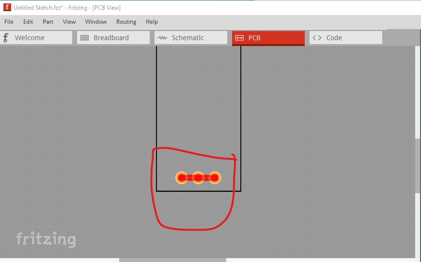
No your part isn’t correct as we see from pcb view:
the red bar over the connectors indicates a problem with connectors. In this case because connectors11 and 12 are present but 0 height and width in the svg. The correct way to do this is detailed in this howto:
The way I would do this is by editing the .fzp file (AFAIK this can’t be done in parts editor, you need to edit the files):
edit part.ACS712_work_8623c1fd6cd1466e860cdcc20a7ca8dd_4.fzp with a text editor and change:
<connector type="male" name="A/C" id="connector11">
 <description>A/C</description>
 <views>
  <breadboardView>
   <p svgId="connector11pin" layer="breadboard"/>
  </breadboardView>
  <schematicView>
   <p svgId="connector11pin" terminalId="connector11terminal" layer="schematic"/>
  </schematicView>
  <pcbView>
   <p svgId="connector11pin" layer="copper0"/>
   <p svgId="connector11pin" layer="copper1"/>
  </pcbView>
 </views>
</connector>
to
<connector type="male" name="A/C" id="connector11">
 <description>A/C</description>
 <views>
  <breadboardView>
   <p svgId="connector11pin" layer="breadboard"/>
  </breadboardView>
  <schematicView>
   <p svgId="connector11pin" terminalId="connector11terminal" layer="schematic"/>
  </schematicView>
  <pcbView>
  </pcbView>
 </views>
</connector>
and repeat this for pin12. This suppresses the connectors in pcb view as desired. The same thing will work in the other views as well.
Peter
