this is a continuation of
https://forum.fritzing.org/t/part-creation-howto-part7-suppress-pcb-layer-howto/7918/
Here we are going to look at the correct layout of the various svg files, because I saw a post from someone that had at least tried to make their own new part before asking for help, that couldn’t figure out the copper layers in pcb. Someone else requested a howto using the parts editor (I think perhaps thinking that parts editor would avoid the use of an svg editor which is unfortunately not correct.) So here I am going to start with a part created from the Parts editor (rather than my usual practice of creating one from scratch) as that is the recommended way to do this. I’ll then at least try and finish the part with the parts editor (although I am usually not successful at that.) The new Parts editor was not completed when development stopped, as a result there are a number of things it won’t do, and probably a number of bugs and I tend to not use it, but it does have the advantage of producing the necessary svgs correctly (if messily) formatted for a new part. It also allows you to set the metadata easily via the metadata tab, so I sometimes do that. To kill 2 birds with one stone, someone recently requested a part for a osoyoo Lora Module, so I am going to make such a part starting from the new Parts editor. The starting point is a google search for "osoyoo lora module: to find a data sheet which led to this web page:
http://osoyoo.com/2018/07/23/osoyoo-long-distance-wireless-transceiver-uart-lora-module/
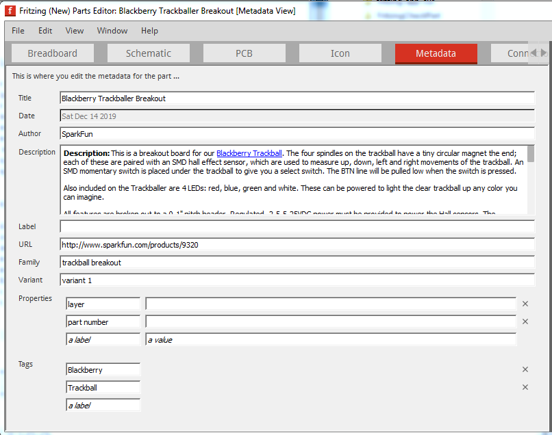
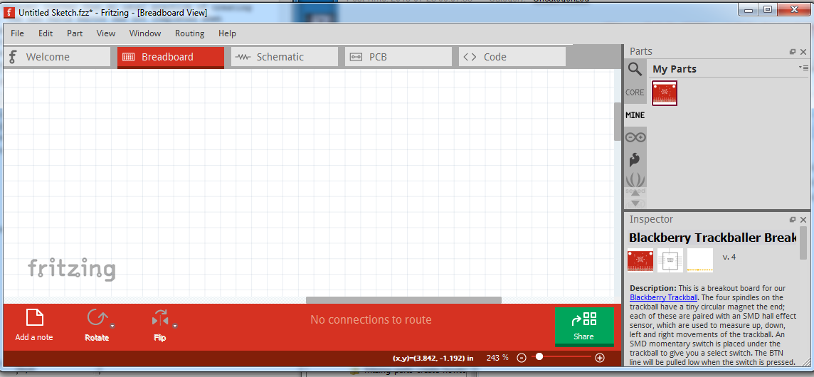
which looks to have the needed data: size of the module, and a mechanical drawing of the connectors (quite unusual for these modules!). It isn’t clear that the 3 connections on the right (which are undocumented) are needed, but I will include them anyway in case they are. There are images of a fritzing part for this module (but no actual .fzpz file I can find) which only have the 7 left side connectors populated. To find a suitable part to clone I started Fritzing and entered “wireless” in the parts search bar and hit enter. That brings up the various wireless modules (and a few oddballs.) Note parts editor will not create parts. You must start from an existing part that has svgs with the appropriate number of pins defined, then edit those svgs with an svg editor to change the svg to reflect the part you want. After that is done the parts editor will configure the fzp file from a graphical interface, but does not edit svg files (it will modify the text of an existing svg file but that is all.) Turns out one of the oddballs: Blackberry Trackballer Breakout is the closest to what I want: 11 connections with pcb as .1in header connectors, so start from that. Select it in the search parts bin and right click on it. Select Edit Part (new Parts Editor) which brings up the new parts editor with the part loaded. Select the meta data tab from the top left:
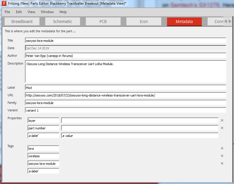
modify the meta data to this from the data sheet:
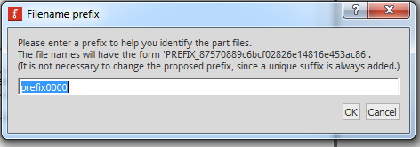
then File->Save as new part and this comes up:
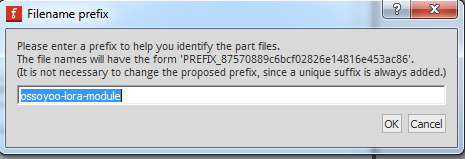
Change “prefix0000” to “ossoyoo-lora-module”
then click OK which changes to the main Fritzing window with the new part in the mine parts bin:
At this point you can close the new parts editor (saying don’t save to the prompts til it closes.) At this point you have all the required files for the part in the fzpz file in the mine parts bin. Now I am going to proceed to edit all the files (if you want to use parts editor, you only need to edit the svg files below, the fzp file can be modified by parts editor.) First you need to export then unzip the part as a .fzpz file. So right click on the new part in the mine parts bin and select Export Part and save it in an appropriate directory. You can now close Fritzing again answering don’t save to all the prompts. Now change to the directory where you saved the fzpz file and unzip it. That will give you the following 5 files:
part.ossoyoo-lora-module_dfdc540f3e4633ed4bfde16ac4e28d7e_1.fzp
svg.breadboard.ossoyoo-lora-module_dfdc540f3e4633ed4bfde16ac4e28d7e_1_breadboard.svg
svg.icon.ossoyoo-lora-module_dfdc540f3e4633ed4bfde16ac4e28d7e_1_icon.svg
svg.pcb.ossoyoo-lora-module_dfdc540f3e4633ed4bfde16ac4e28d7e_1_pcb.svg
svg.schematic.ossoyoo-lora-module_dfdc540f3e4633ed4bfde16ac4e28d7e_1_schematic.svg
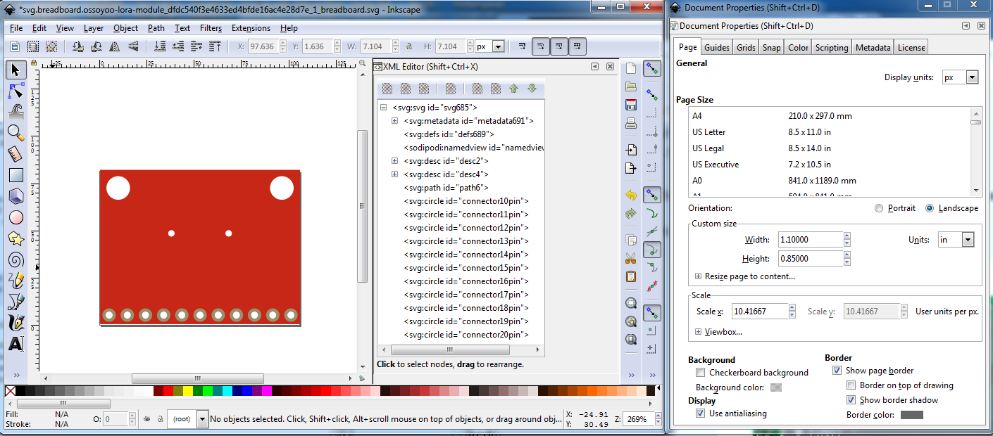
We are currently interested in the four .svg files (actually the icon file isn’t interesting and will be replaced by the breadboard svg file later.) Lets start with the breadboard svg by opening it in Inkscape which gives this:
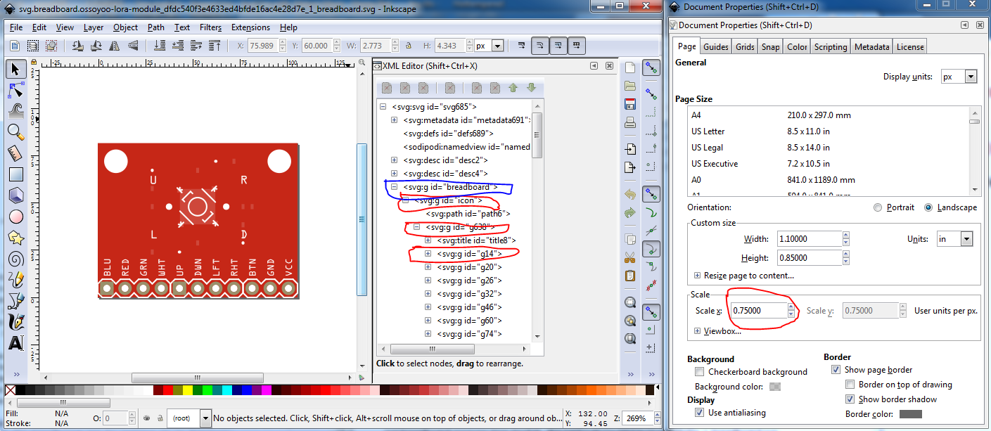
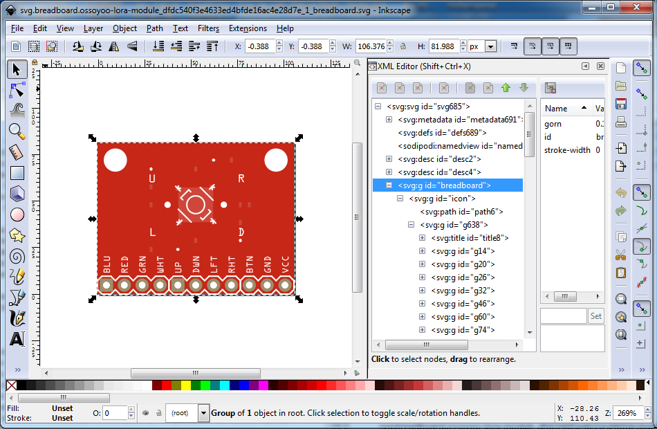
Several things of note here, the svg is scaled wrong (0.75 rather than 10.41667), it has a correct layerId of “breadboard” as the top group (it could also have a group such as g25 below which is a group called “breadboard” and still be valid, but it must have a group with the id “breadboard” with the breadboard drawing elements below it to be correct.) It also typically of Parts editor svgs, has many subgroups. They don’t affect anything (except possibly performance in a probably small way) and can be useful to group sections of the svg, however I prefer to remove all groups except the layerId group (“breadboard” in this case) and because we want to rescale this document we first need to remove all the groups (because rescaling reacts poorly to groups.) So select group breadboard like this:
then either click Object->ungroup multiple times, or as I prefer use the keyboard shortcut cntrl-shift-g multiple times to ungroup the entire document. If groups are present Inkscape will use transforms when you move elements and transforms are undesirable (because they imply an expensive to performance matrix multiplication to render.) Doing that results in this:
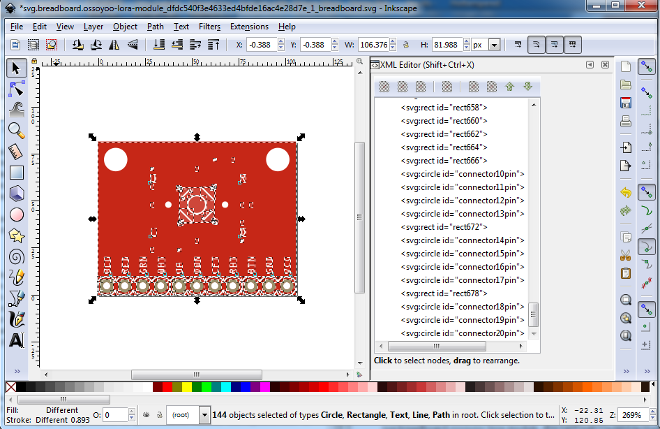
which turns up another problem: the 11 connectors do not start at 0 as they should, but rather at 10. So we need to renumber the connectors as well as rescale the document to start our new part. Now refer to the rescale howto here:
https://forum.fritzing.org/t/rescale-a-svg-using-inkscape/7581
to rescale the svg to 10.41667 then delete everything except the connectors (because the connectors are all that we want out of the original svg) to give this (the path6 that makes the rectangle and the holes should be deleted too, but I left it in here to show everything else that has been removed because without the path the white lines will still exist but be invisible against the drawing window and they need to be removed too!):
Now create a rectangle to be the board of the lora module, and set its height and width according the module size in the data sheet (i.e. 21mm wide by 36mm high, then move it to the top so the connectors show on the rectangle and set the fill to green to match the board. Now we need to position the rectangle according to the mechanical drawing. To that end I copied a line from the schematic svg in to the breadboard svg via copy/paste, then set the new line (via xml editor and the toolbar to be as wide as the connectors, black, and with a stroke width of 1 (1/1000 of an inch.) like this:
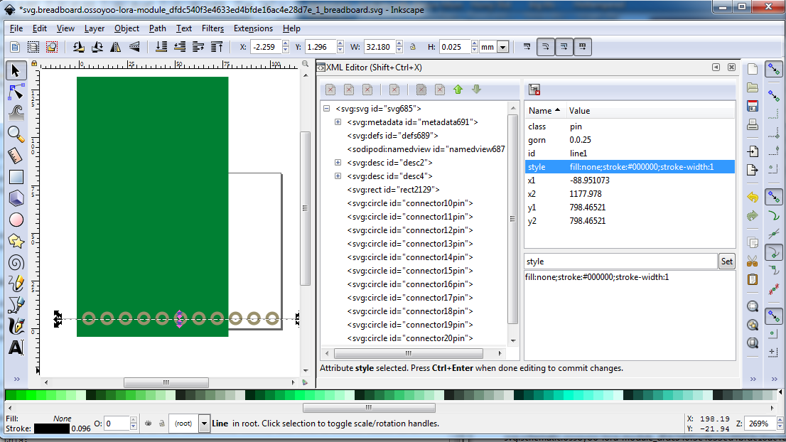
Now duplicate the line, and rotate the duplicate 90 degrees and move both lines so they match the center of the first pad as the measurements in the mechanical drawing are to the center of the connectors like this:
Now move the x and y position of the green rectangle until the distance from the center of the connector matches the offset from the mechanical drawing, in this case 1.5mm from the bottom of the rectangle to the horizontal line through the connector and 2.88m from the left edge of the rectanlge to the vertical line through the connector. To make calculations easier I did an edit select all and resize page to drawing to make all coords positive before doing the calculations, that results in this:
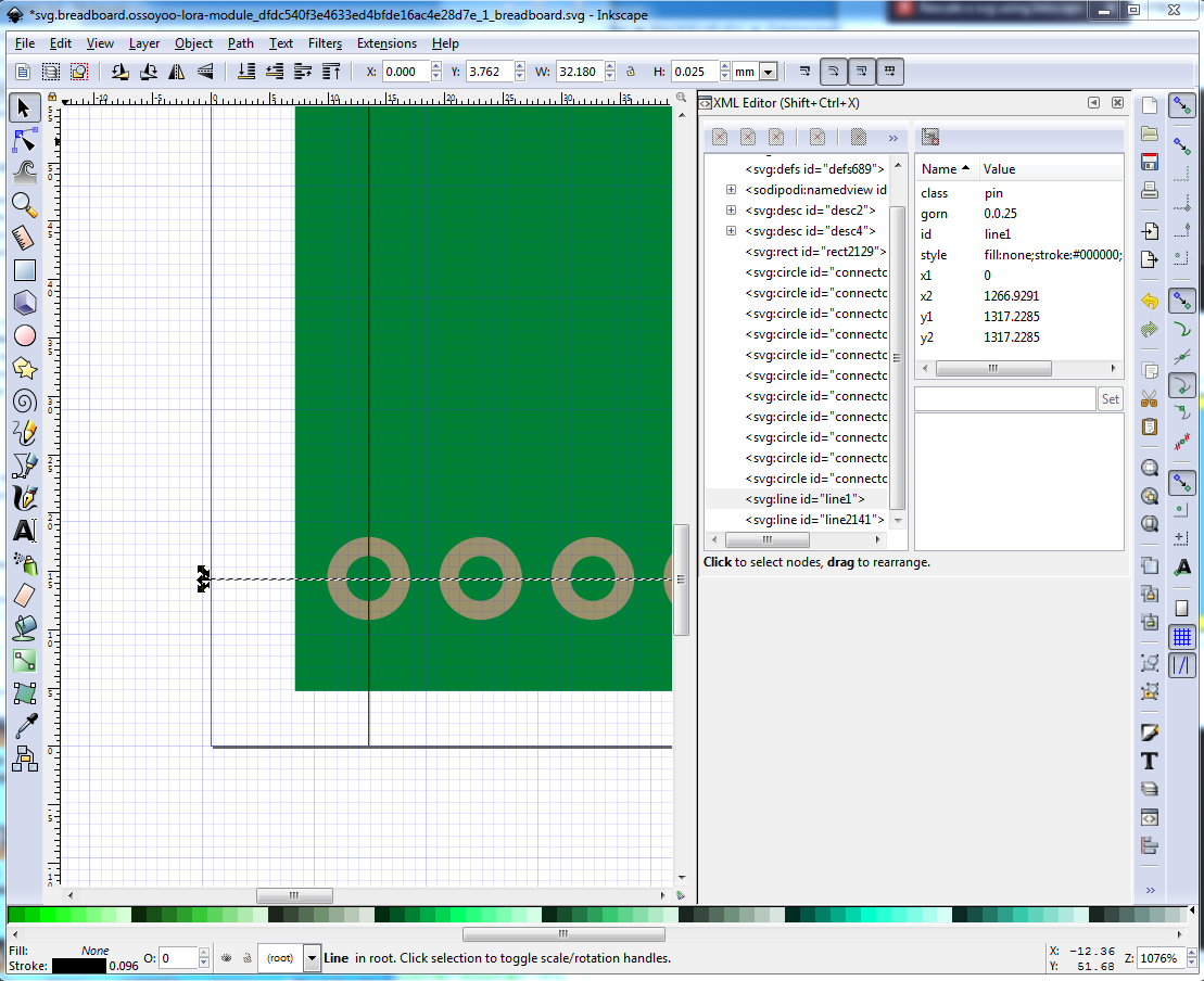
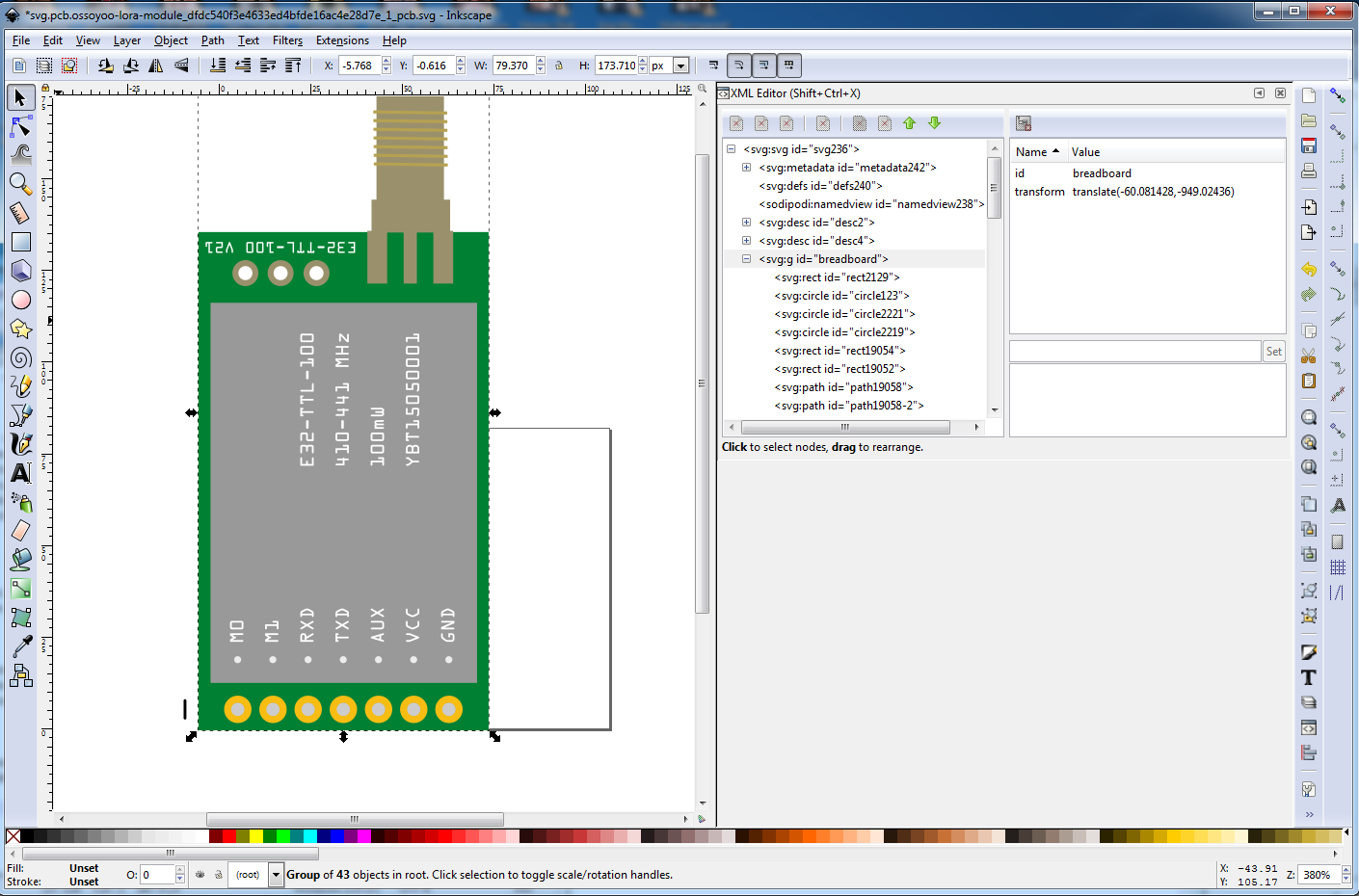
here the horizontal line is at 3.762mm in y, the bottom of the rectangle wants to be 1.5mm lower than that or 2.262mm so set that as the rectangle’s y coord. The vertical line is at 3.572mm, so the left edge of the rectangle wants to be 2.88mm less than that or 0.692mm so set its x coord to that. Now we delete the 8th pad (as unused) and move the 3 remaining pads to the top of the rectangle for the unknown connectors. To position them, duplicate the horizintal line and add 31.5mm to its y coord to give the center of the three pads at the top or 35.262mm. Duplicate the vertical line and set its x coord to be 3.46mm from the left edge of the board or 4.152mm. Now center the left most of the top 3 pads on the two new lines, then set the other two .1in further along in x to set the postition of the top three pads. That leaves the sma connector for that antenna to source and place. I happen to have made an SMA connector for someone in the past (it is posted in parts help in the forums if you do not have one) so I did a copy / paste of its breadboard (after removing the connectors which aren’t wanted in this application) and copied it in to the svg. Positioning it is somewhat painful because you have to add up the various offsets to the conncetors to get the distance from the left board edge the start of the SMA connector as 12.942mm. Then we need a rectangle (with no dimensions on the drawing so guess!) of the radio module. Once that is done set small circles at each pin position to mark the text to the pin. Then create the text for the labels on the pins and the text on the module from the photo in the data sheet. I usually do a copy / paste of text that is correctly configured from another braadboard, then modify the text to requirements (and that is what I did in this case.) With that done, remove the construction lines as no longer needed and clean up the connectors. The board to this point looks like this (with the first connector to be cleaned up selected):
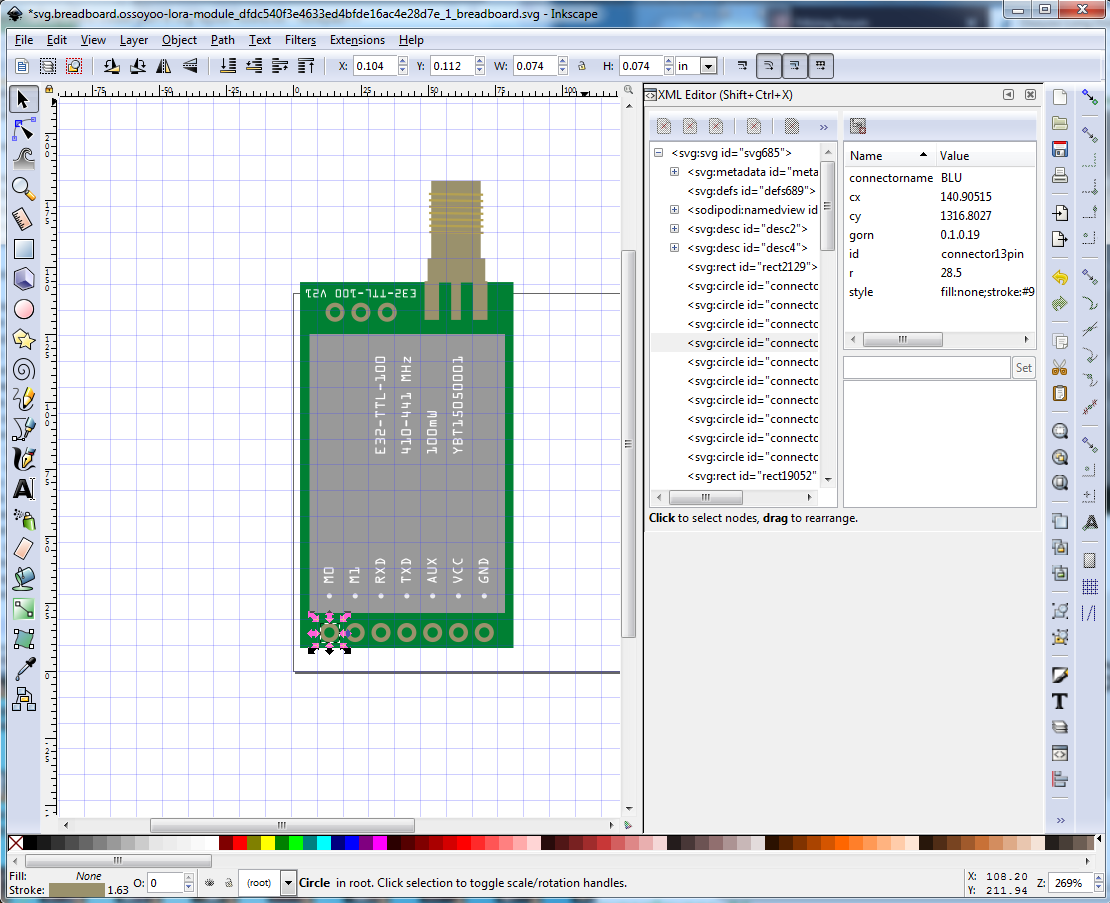
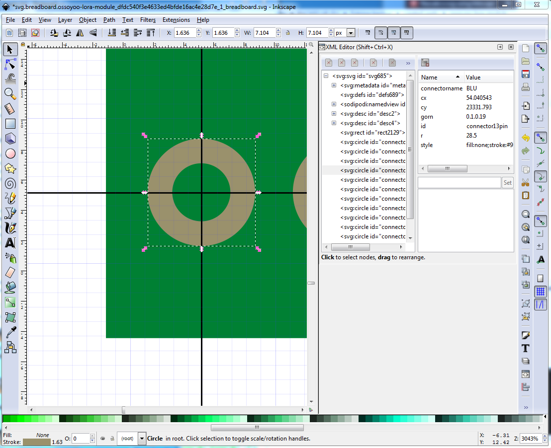
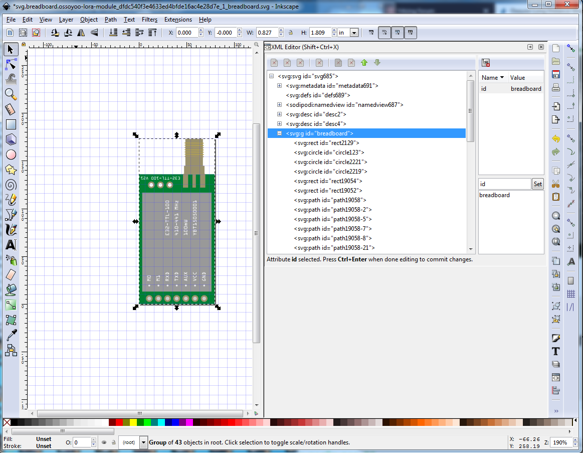
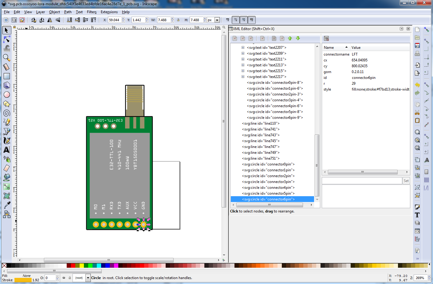
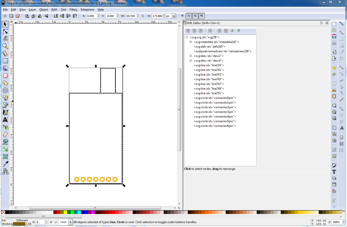
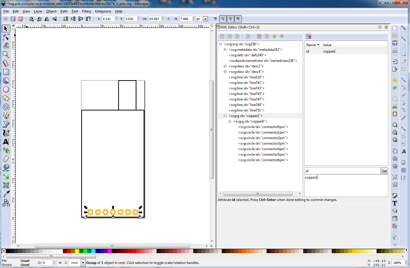
Here we see a number of issues: there should be a solder tab instead of green in the center of the connector, the circle was an ellipse (I had corrected this one before this image), and the connectorId is incorrect. So fix all of those problems like this. Solder tab: change the fill of the connector from green to silver. Change the id in xml editor from connector13pin to connector0pin, set rx and ry in xml editor to 28.5 to make it a circle again. Then repeat this for all the rest of the other 6 in use pads (increasing the pin number by 1 each time.) Once all the 7 bottom connectors are done, we need to move on to the top 3 connectors. Since we don’t know what (if anything) they do, we will not assign them pin numbers at this time, just leave them as circle123 with a white center to indicate there is a hole there. Now to finish clean up start with connector0pin and click the move to bottom icon on the tool bar to move it (and the 6 other connectors in sequence) to the bototm of the xml window. Functionally this makes no difference, but it makes finding the connectors easier for humans and is thus a good practice to adopt. Now all that remains is to do an Edit-> select all, Resize page to drawing or selection, to adjust the viewbox to match the finished image. Then with Edit-select all still active either cntrl-g or Object->group on the tool bar to group the entire image, then in xml editor change the id of the group just created to breadboard to set the required breadboard layerId. Now File->save as and select plain svg and save (clicking OK to replace) and breadboard is complete and looks like this:
On to schematic. As usual schematic is the wrong scale and unsuitable for the current part, so as usual I chose to replace it with the properly scaled schematic template file from schematic template howto here:
https://forum.fritzing.org/t/schematic-svg-template-howto/7583
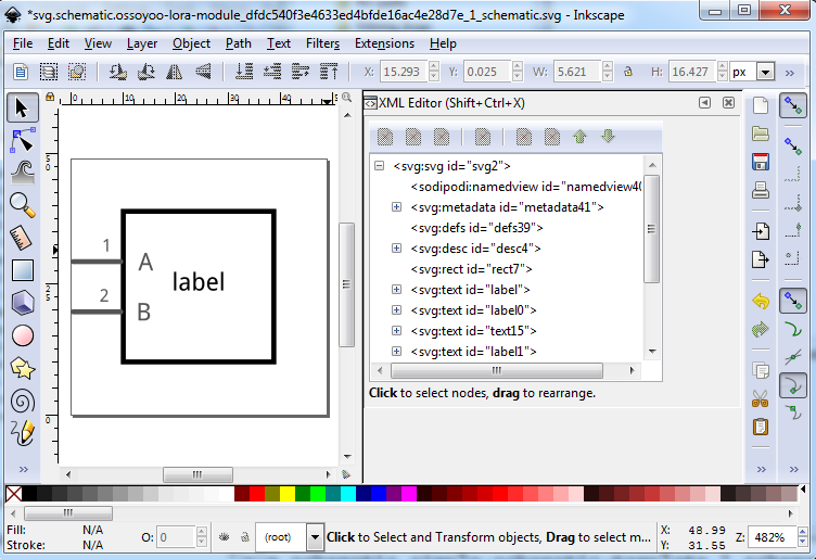
So copy svg.schematic.simple-schematic-template_1_schematic.svg from the above howto in to the svg.schematic.ossoyoo-lora-module_dfdc540f3e4633ed4bfde16ac4e28d7e_1_schematic.svg file and edit it in Inkscape. Delete the pins on 3 of the sides leaving an svg which looks like this:
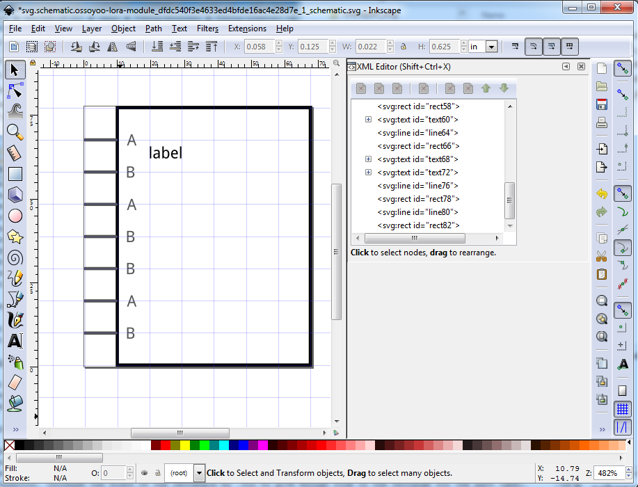
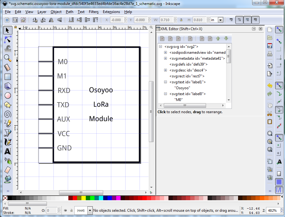
then set the dimensions from px to in and enable the page grid (View->Page grid) and duplicate the existing 2 connections and move them down in y til there are 7 pins on the left side of the rectangle. Then move the rectange down til it is .1 in below the last connector and increase its height until it is .1 in above the first connector. Increase the width of the rectangle by .3in to give enough room in the rectangle for the part label. The end result should look like this (after doing and Edit->select all and resize page):
Since in theory parts editor should be able to set terminalIds from a pin, I chose to delete all the terminalIds (the rectangle on the end of the pin) from the svg and will try and add them via tha parts editor later. So click on the line that connects to the RXD label and set its id field to connector2pin from line52 in xml editor. Repeat this (increasing the pin number by 1 for each pin) for the next 4 line. Now click on the text “label” and change its id from label to label1 (to avoid text substitution which we don’t want.) Then set its text to be “Osoyoo” duplicate it, and move the duplicated text down .1in in y and set the text to “LoRa”, repeat this and change the text to “Module”. This should end up looking like this:
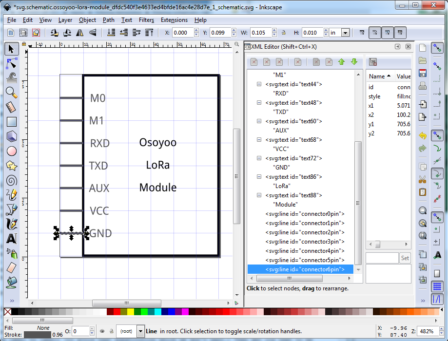
Now we are going to clean up a bit and save this. First as in breadboard, select the connectors one at a time starting with connector0pin and move them to the bottom of the xml window so they end up looking like this:
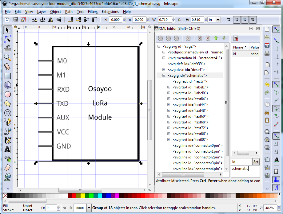
Now Edit->select all and resize page to drawing or selection to reset the viewbox, then group (cntrl-g) and change the id of the group to schematic to end up with the finished svg which should look like this:
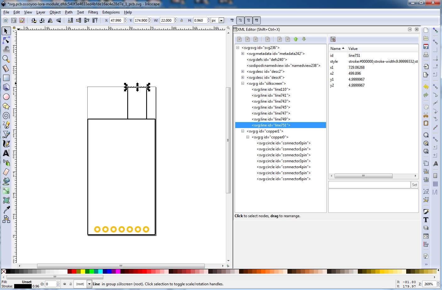
then File->save set the type to plain svg and save it (answering yes to replace the existing one) and schematic is done. Now on to PCB, so edit svg.pcb.ossoyoo-lora-module_dfdc540f3e4633ed4bfde16ac4e28d7e_1_pcb.svg in Inkscape where we find the scale is again 0.75 instead of 10.41667 so ungroup the entire svg and rescale it to 10.41667 as we did from breadboard to produce (note I cheated here and ran the pcb svg through the check part script to covert the silkscreen from white to black so the silkscreen lines will show up in Inkscape.):
Of interest here is the x and y origin values are not 0 (and it is possible the lines on silkscreen will be truncated as a result) so first do a Edit->select all and resize page to content to set the origin to 0 0 before rescaling. Now rescale the svg as we did for breadboard. Now delete all the silkscreen items except for the 1 line which will make up the new silkscreen and the last 4 pads as unneeded. Starting with the leftmost pad select its id and change it from connector13pad to connector0pin. Repeat this down the line of pads (increasing the pin number by 1 each time.) Then select connector0pin again and look at xml editor which should look like this:
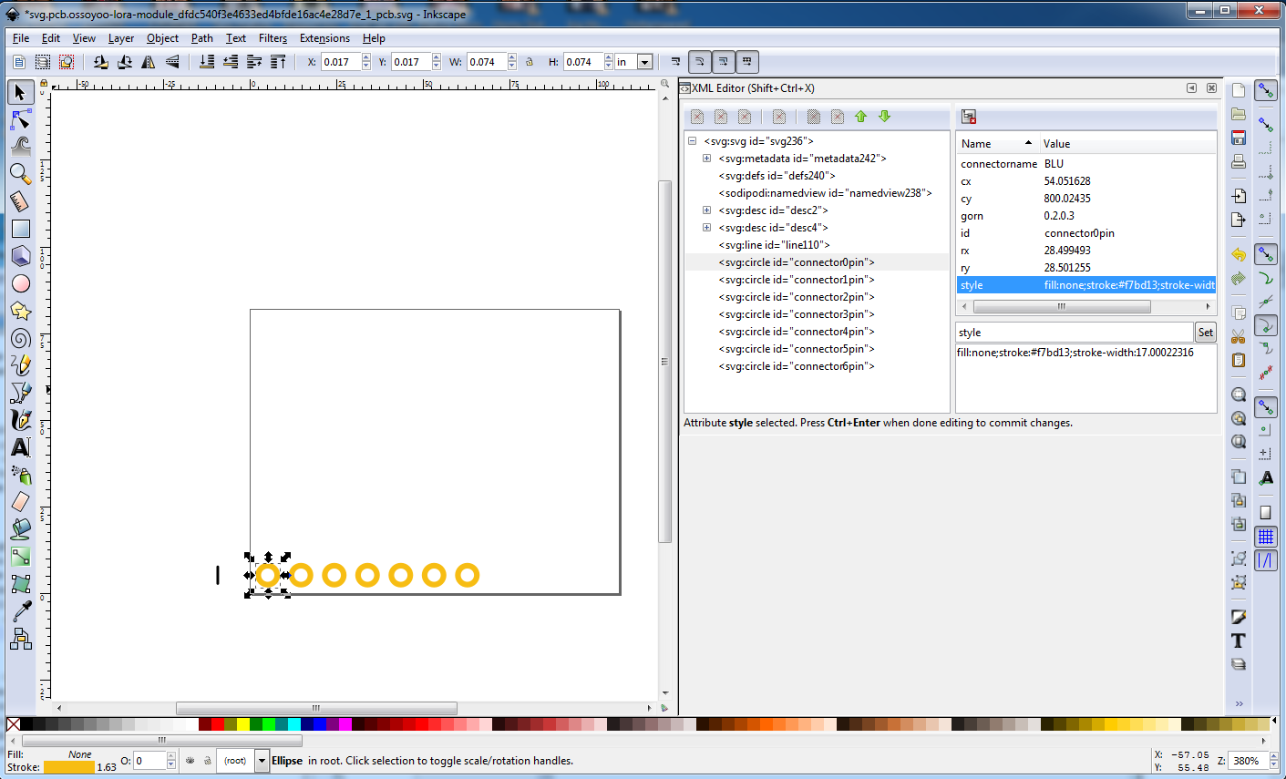
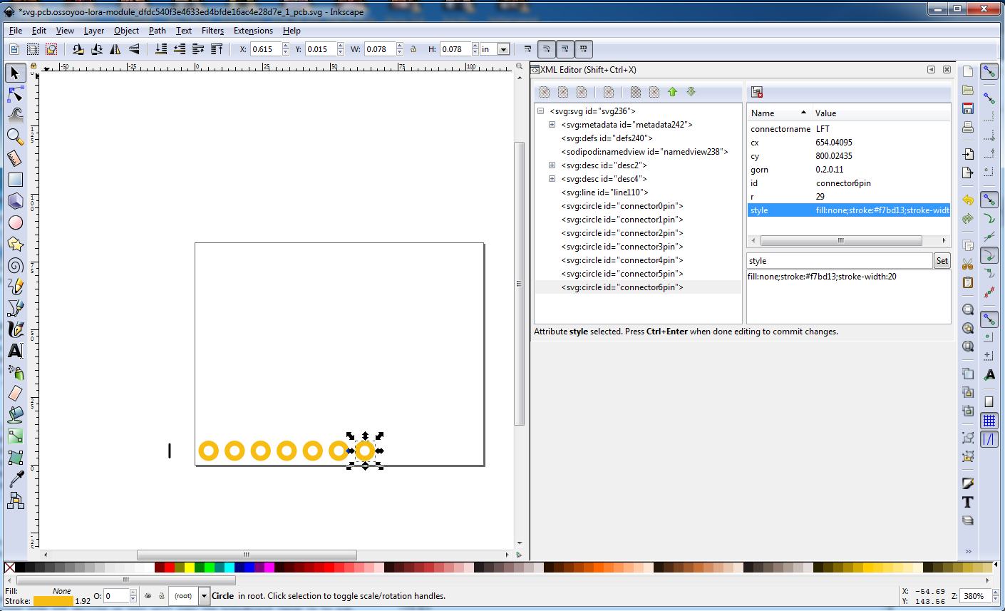
There are several things wrong here that need to be corrected. The radius is incorrect, both from the rescale and because the original svg was incorrect. For .1in headers as configured here, the hole size should be 0.038in, which at a scale of 10.41667 and with a stroke-width of 20 equates to a radius value of 29. At present the stroke-width in the style command highlighted is 17.00022316 not 20 so we need to replace that with 20 in all the pins. Then we need to change the radius values to 29 for both rx and ry on every pin (this will cause the rx and ry values to replaced by a r 29 which is what the gerber code requires to drill the hole.) This is the corrected svg with all the pads correct:
Now we need to do the silkscreen. In this case (as in most cases) the easy way to do that is to do a copy / paste of the breadboard svg in to pcb like this:
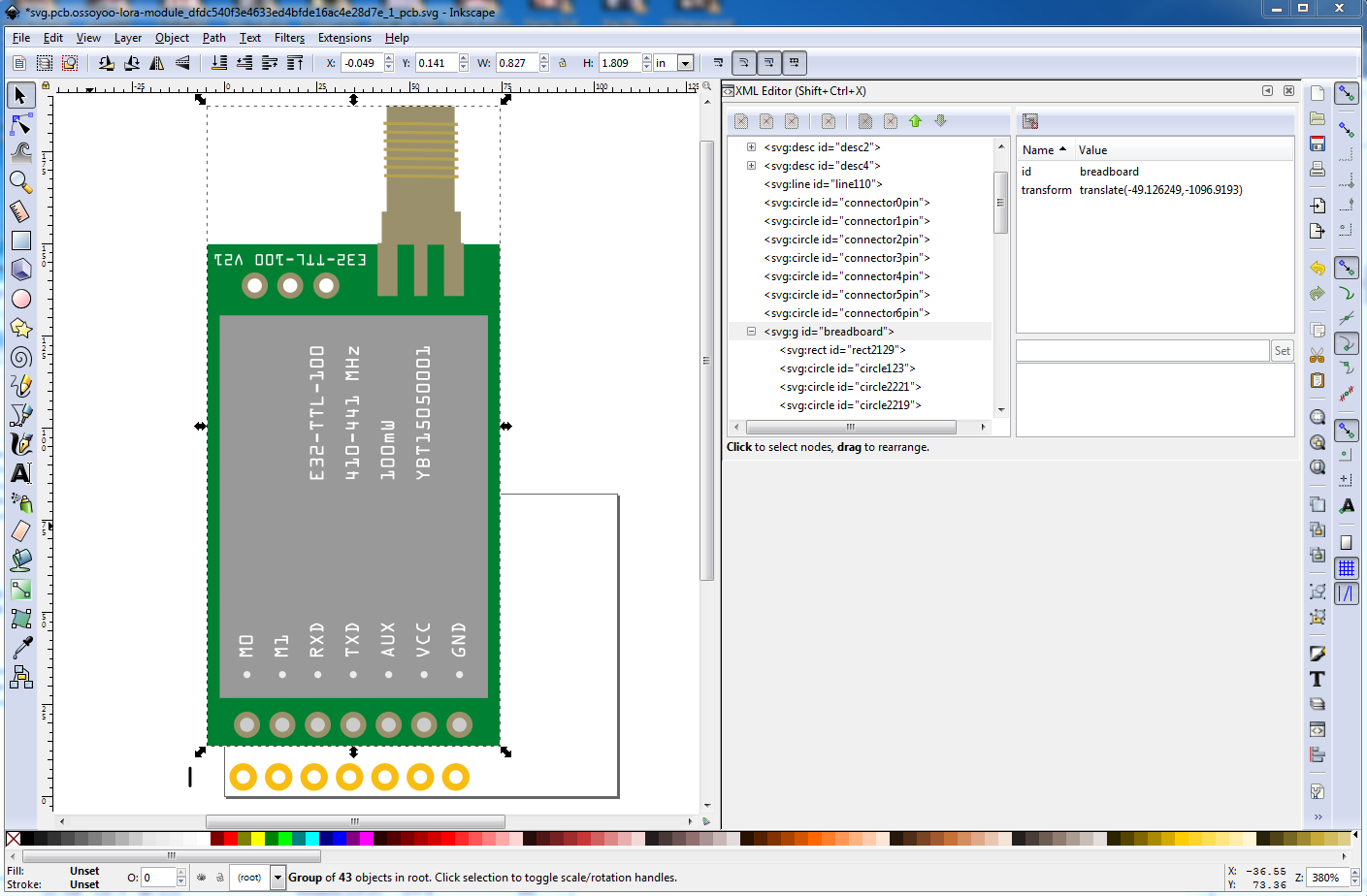
here do an Edit->copy to copy the breadboard completely to the clip board. Then switch back to the pcb svg and do an edit->paste which (if the Inkscape gods are smiling on you) will copy the breadboard image in to pcb, leaving it in a group called breadboard for easy deletion later. The result should look like this:
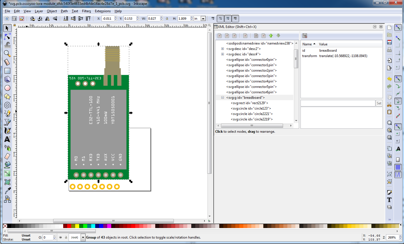
First, select the breadboard group and move it to the top so that the pcb connectors appear on top of the breadboard image. Now move the breadboard image until the connectors overlap like this:
now using the silkscreen line we saved, outline the rectangle of the breadboard image with silkscreen lines to produce the needed silkscreen outline like this:
then delete the breadboard group to leave the pcb and silkscreen like this:
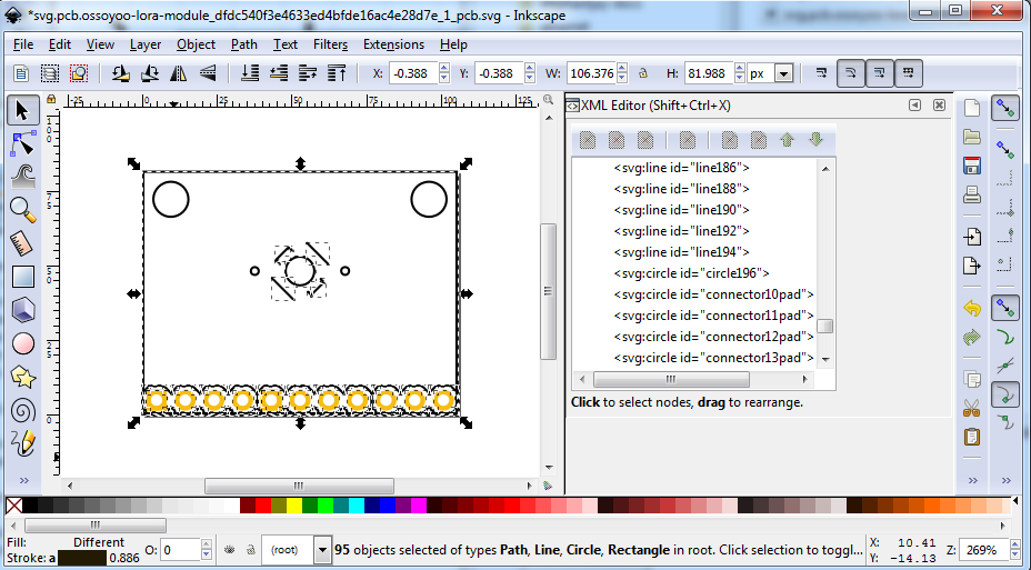
now it is necessary to add the needed pcb groups. They are (at a minimum as here) silkscreen, copper1 and copper0 (which is a subgroup of copper1.) Other configurations are valid and more groups are possible, but for a basic part this is the minimum and usual setup. First we select all the connectors and group them twice (once for copper1 and the second time for copper0) then change the group ids to copper1 and copper0 like this:
Now we need to group all the lines in to the silkscreen group (which wants to be above copper1/copper0 to aid in the selection process in Fritting) like this:
We now save this file as plain svg to complete the pcb svg. While this is the minimal correct pcb configuration for a through hole part, many other configurations will work (they are just more confusing to look at.) As noted the parts editor loves groups and will produce large numbers of nested groups at times. Somewhere in the set of groups you should find a silkscreen group, a copper1 group and a copper0 group (hopefully under copper1.) I find it best practice to ungroup such a svg and then regroup it in to this configuration to make the structure clear. At this point we have the 3 svg files (and an fzp file, which I suspect is going to be broken because I changed the pads in the pcb svg to be pins and changed the pin numbers but we will see) and can now go back to the parts editor to make the new part. Note there is no magic easy button to make parts, you have to go through the above process to make the 3 svgs (breadboard, schematic and pcb) needed by parts editor to make a part. As noted parts editor will not produce the svg files, you need to do that using an svg editor. The parts editor will adjust the fzp file for you, (as noted I usually find it easier to edit the fzp file with a text editor, but this time I am going to attempt that with the parts editor and see what happens.) Start Fritzing and load the ossoyoo-lora-module.fzpz part I started from in to Fritzing in the mine parts bin and right click on it and select Edit with bew parts editor. The editor comes up as expected, so now let us try and load the new breadboard svg we created in to parts editor. To do so, click on breadboard view which currently looks like this:
so now select File->Load image for view and select the new breadboard svg we made above:
doesn’t look much like the bb svg we last saw above. So exit this, and run that svg through the FritzingCheckPart.py script (which I hadn’t yet done) to remove the px from font-size (one possible cause of this failure) and inline the style commands (not as likely a cause) then try again. Yep, looks like the parts editor doesn’t like px in font-size (Fritzing doesn’t either, that’s why FritizngCheckPart.py removes them) this time the svg looks correct:
on to schematic (only this time I will run the svg through check part first) works correctly:
then pcb which also works:
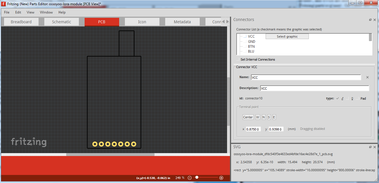
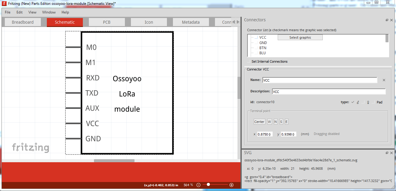
Now to try and set the connectors via parts editor. So change to the Connectors tab in Parts editor. First problem, there doesn’t appear to be a way to change the connectorId. It appears to have taken the connectorIds from the fzp file (which in this case is incorrect, starting at connector10 instead of connector0 as it should.) It appears the only solution to this is to manually edit the fzp file to correct the pin numbering. Given that you have to hand edit the fzp file anyway, I don’t see a point in not doing the entire fzp file manually and thus don’t see any advantage to using the Parts editor to make parts. Here is the original fzp file (where connectors start at connector10):
part.ossoyoo-lora-module_dfdc540f3e4633ed4bfde16ac4e28d7e_1-orig.fzp (7.9 KB)
and here is the manually corrected version of the fzp file which starts the connectors at connector0 as it should:
part.ossoyoo-lora-module_dfdc540f3e4633ed4bfde16ac4e28d7e_1.fzp (5.8 KB)
The problem I see is that the above file in conjunction with the 3 svgs created above when run through FritzingCheckPart.py then zipped in to an fzpz file creates a valid part. There doesn’t seem to be any point to editing it with the Parts editor after fixing up the fzp file manually. If someone who uses the parts editor successfully would point out where I am wrong (if I am wrong) it would be appreciated. The bottom line is that the parts editor (at least in its present state) doesn’t reduce the work of making a part very much.