OLED 128x64 I2C Monochrome Display.fzpz (15.3 KB)
Dear all,
please use improved part from here
https://ajcreatif.com/oled_128x64_I2C_monochrome_display.fzpz
Regards
2 Likes
The hole sizes (0.018in ) in PCB seem quite small. IC pins for instance are usually .035in and .1 header connectors are usually 0.038in. Are the connections really that small?
Peter
The Holes are maybe liittle smaller than Core Headers.
What I notice, that, this part should have through-Hole connectors…!!
Edit: No sorry, the holes are bigger than core headers, But copper is small…
I’m looking at the drill file from the gerber output which is calling for a smaller than usual drill size. The pads are also a little small at .068in diameter (.1 headers are normally 0.078in with a 20 thou pad width).
Peter
Hi all,
I am using this part in my PCB design and have the problem that the Design Rules Check is giving some errors on this part.
Would somebody be able to update this part to have the connectors on both sides and remove the pin names from the copper layer (or move them to the silk layer).
I don’t see text in the copper layer in PCB, but I do see a wrong name for copper0.
I can’t duplicate that text problem - maybe if I had the sketch -,but I fixed the pads.
OLED 128x64 I2C Monochrome Display.fzpz (8.2 KB)
1 Like
Thanks for updating the part. It seems to have resolved both of the issues.
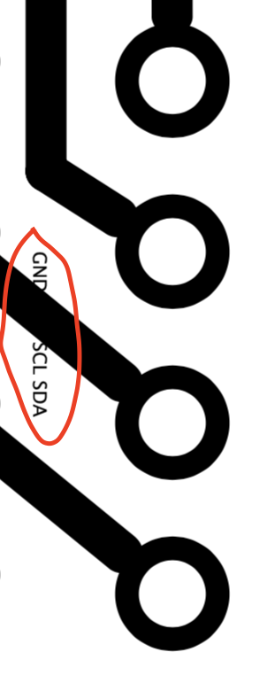
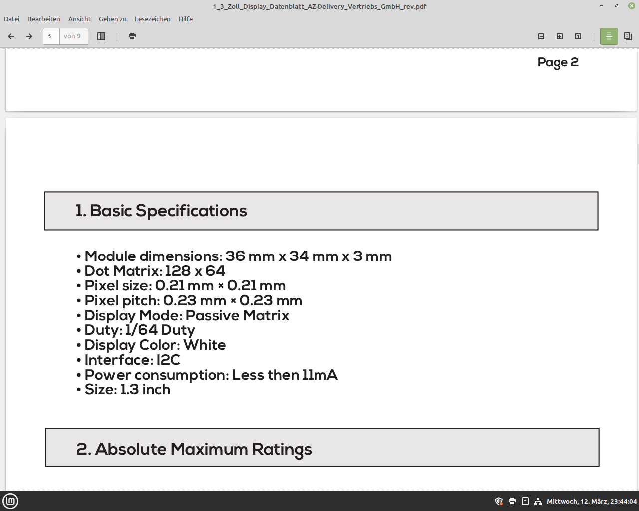
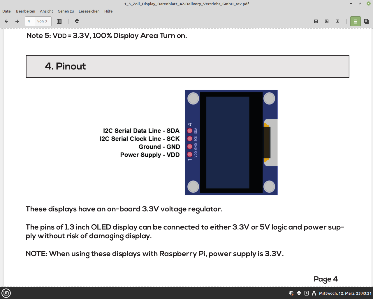
If you plan to use this part, check that the pins match your material first. There are 2 main versions of the SDD1306 OLED 128x64 display, the main difference between them being the VCC and GND pins that are swapped.
In such a case we should make a second part that matches the other common version. Do you have a url to an example of the alternate part?
edit:
A search of Ebay turns up an even mix of both pin layouts so I have made two new parts, one for each pin out. As you noted it is necessary to make sure you have the correct part for the module you have, because using the other one (and reversing power and ground) will likely burn out your module! Note if you want mounting holes in pcb you need to drag a hole over the mounting holes in silkscreen (which will not be drilled!) and set the size of the hole appropriately. The file names contain the GND/VDD pin sequence to tell you which is which.
OLED-128x64-I2C-Monochrome-Display-GND-VDD.fzpz (6.5 KB)
OLED-128x64-I2C-Monochrome-Display-VDD-GND.fzpz (6.5 KB)
Peter
4 Likes
A number of problems here:
-
The file name is invalid on Windows, filenames can’t include ’ " ’ so change it to ‘in’
-
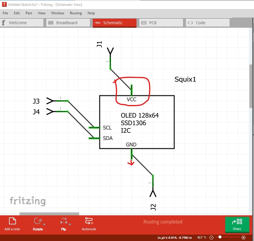
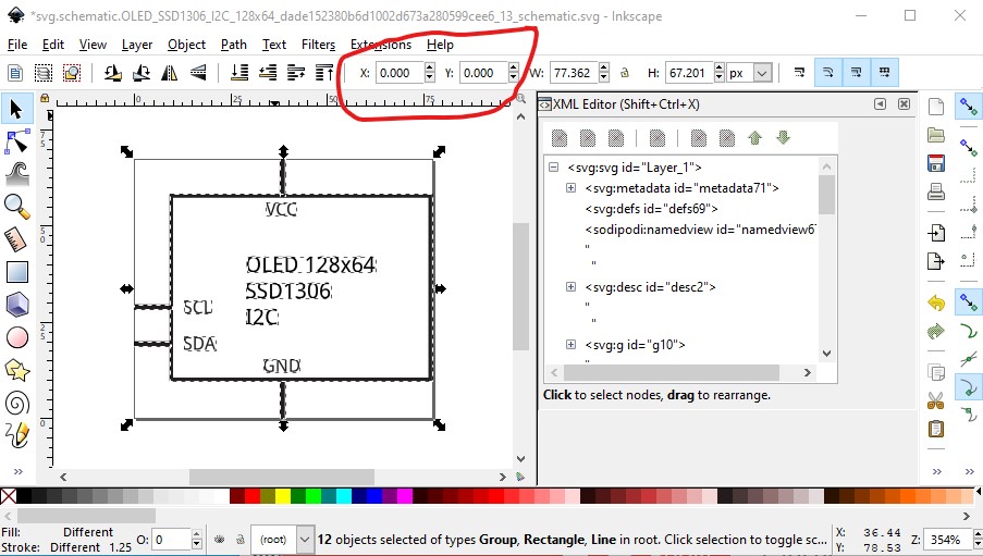
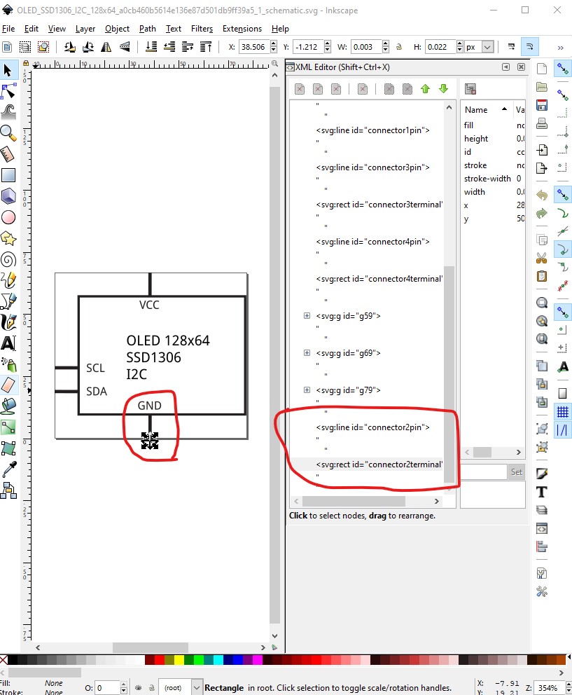
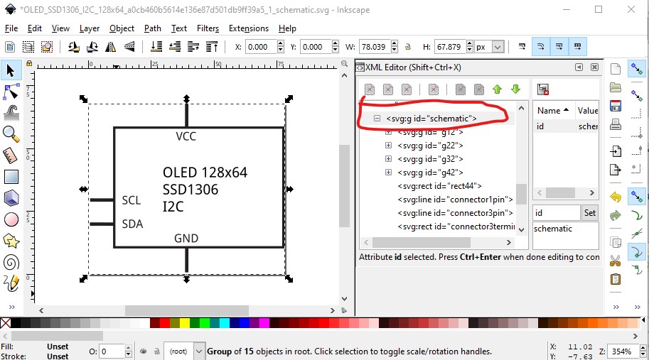
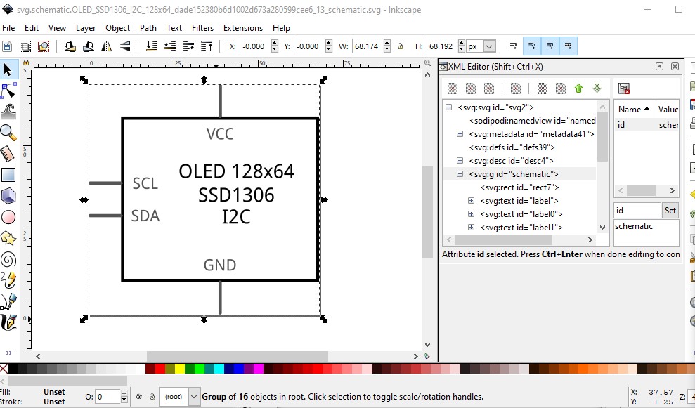
schematic is missing terminalIds which causes the wire to connect in the middle of the pin (circled in red in VCC)
- the pins are not aligned on the 0.1in grid in Y (red arrow on the GND pin)
that is because the viewbox doesn’t start at 0 as Fritzing is expecting:
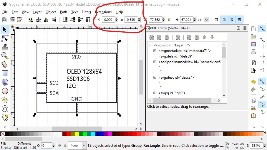
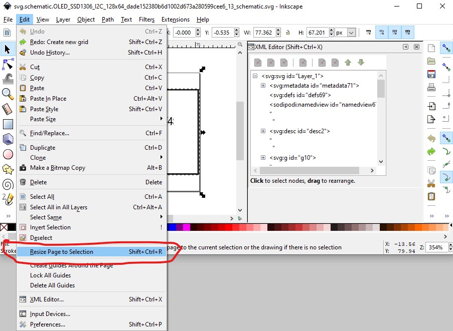
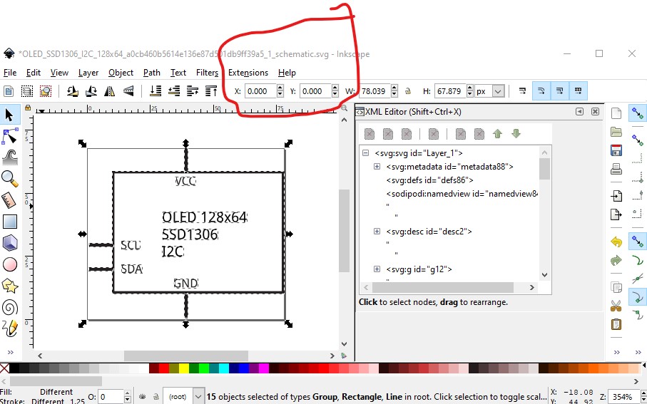
to fix this in Inkscape (I don`t know if you can in Illustrator!) Edit-.Select all then Resize Page to Selection
which changes the origin to 0 0 as Fritzing is expecting.
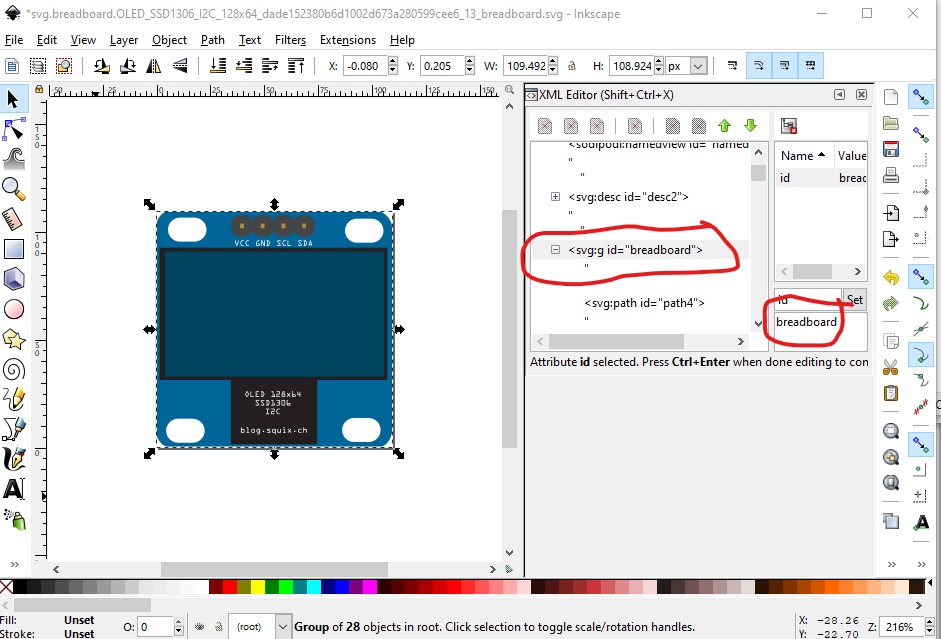
- both breadboard and schematic lack layerIds, that means the part will not export as an image in Fritzing.
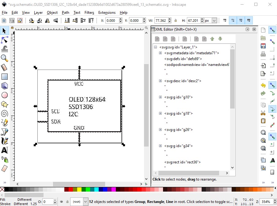
needs to change to this (by grouping the entire image)
then do the same (with layerId breadboard) in the breadboard svg.
Hope this helps!
Peter
1 Like
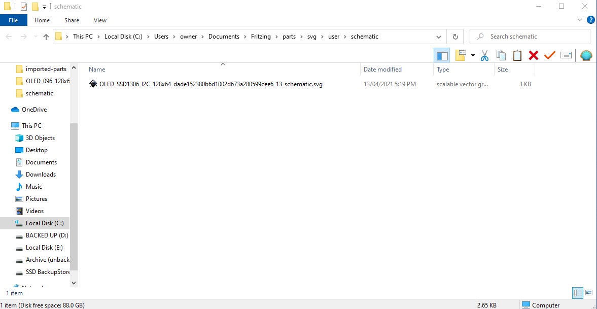
OK here are two ways to do it. Load the current part in to Fritzing, select the part in the mine parts bin and right click and select Edit Part (new parts editor)
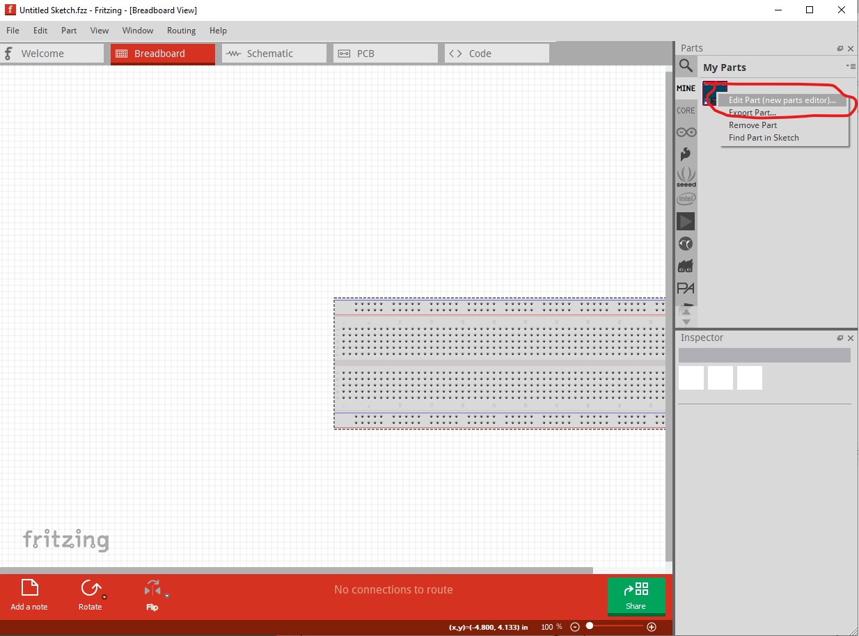
Then click File->show in folder which produces this
click on the svg file to load it in to Inkscape
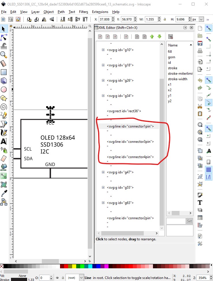
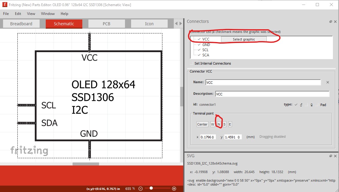
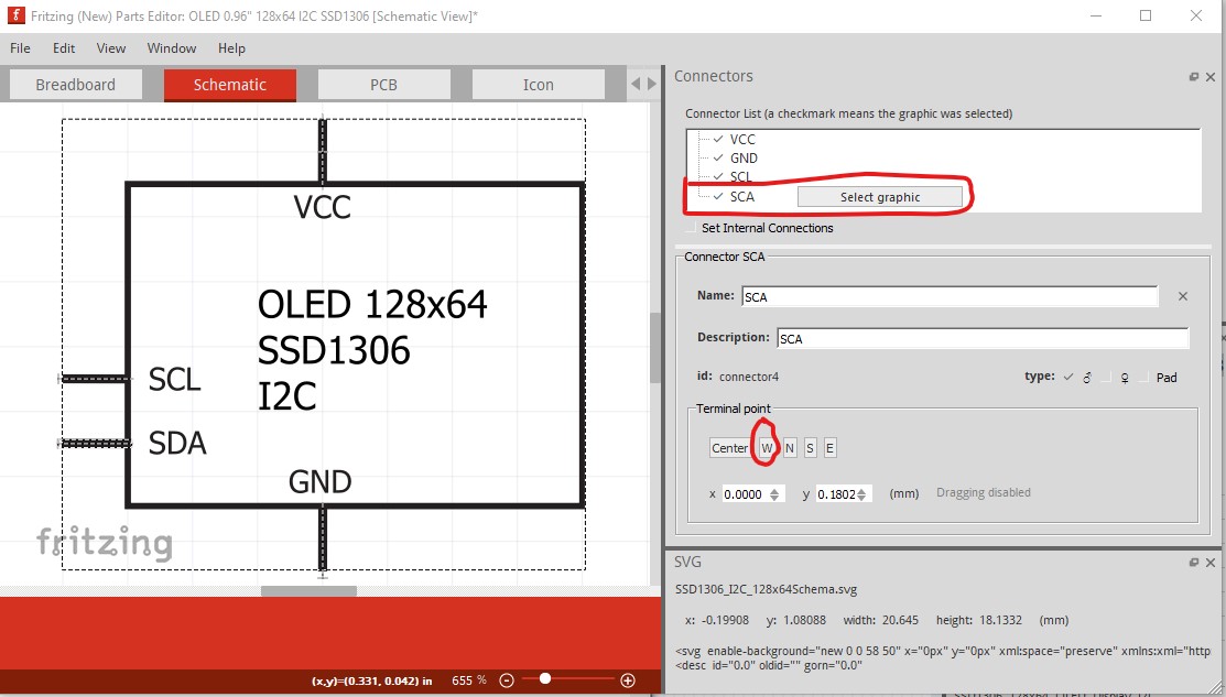
where we see the connectors (1 to 3) pins but no connectorxterminals. Now back to parts editor and click on VCC (circled in red in the image) and then on Select graphic. Then click on N in the Terminal point window below to set the terminalId at the top of the VCC pin (North)
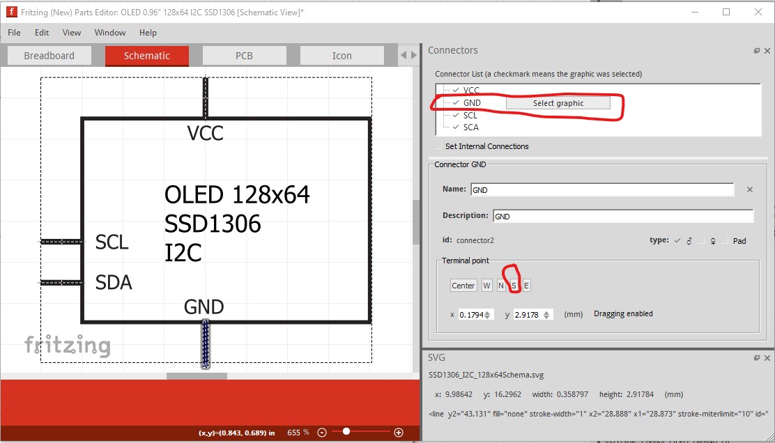
repeat for GND and select S (south) to set the terminal at the bottom of the gnd pin.
Now do the same on SCL selecting W (to set the terminal on the left of the SCL pin)
and last repeat the above for SCA
Now click File->save and OK to the prompt that comes up to save the changes to the part.
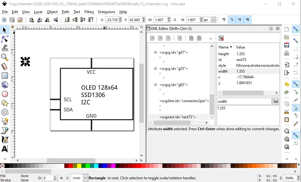
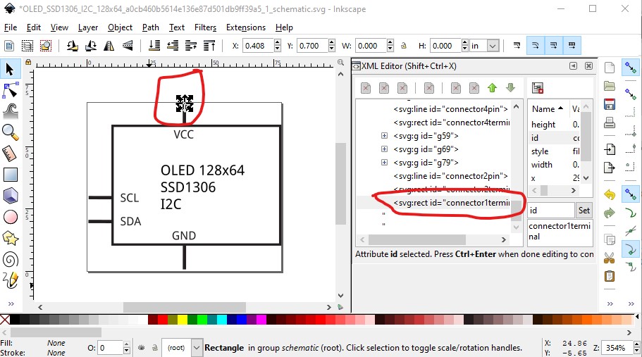
and load the latest one in Inkscape
where we see that connector2 now has a new entry called connector2terminal which is a square positioned at the bottom of the pin as we requested. We also see that the terminal on connector1 is missing (which is one reason I dislike using parts editor!) so we would need to go back and do that one again until it appears.
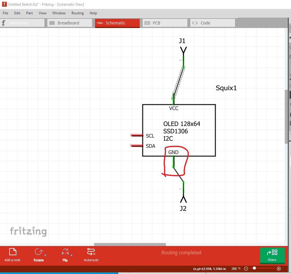
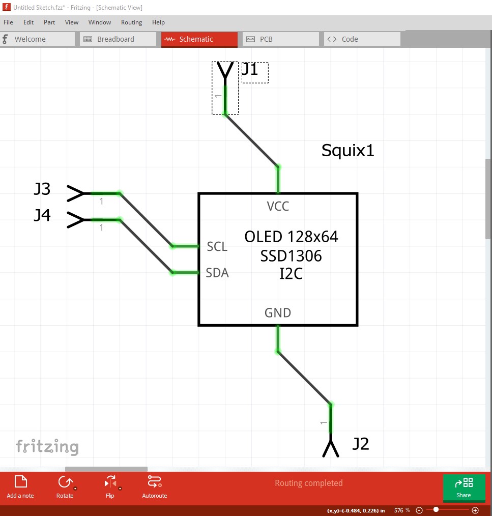
When I now drag the edited part in to the sketch in schematic and connect 1 pin headers to both VCC and GND we see the results (and an error!)
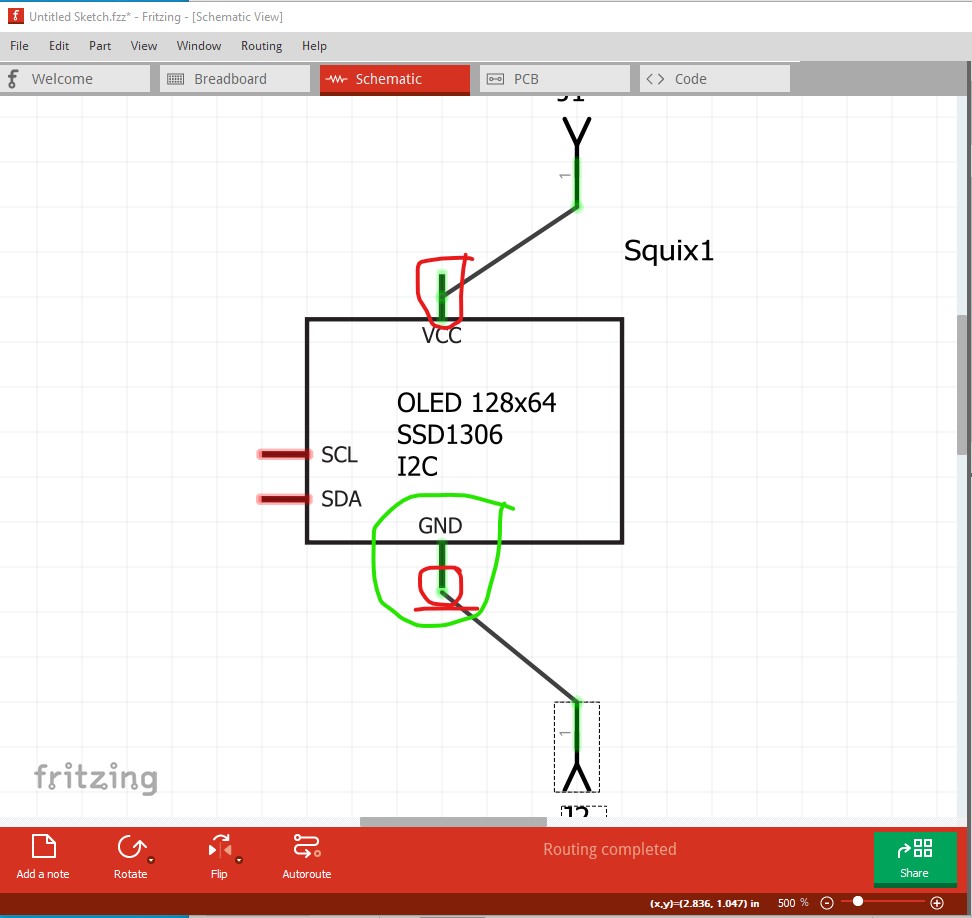
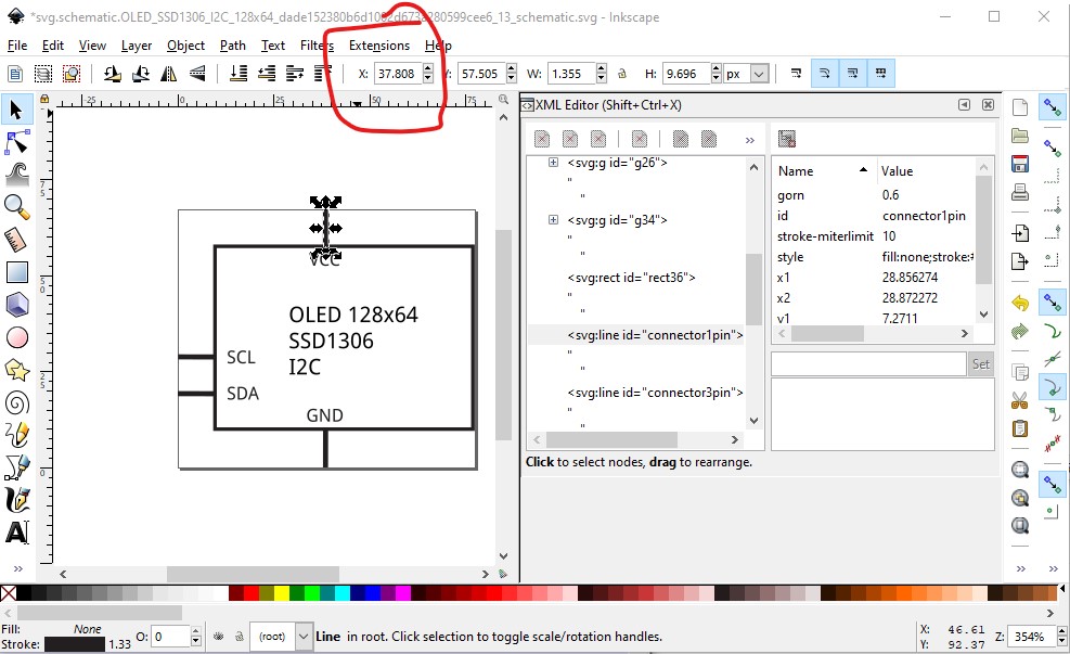
Here we see VCC still connects to the center of the pin (because it has no terminalId) but GND on the bottom connects to the end of the pin as it should. However because the pin has line-cap set to butt instead of rounded there is a small gap between the wire and the pin which is incorrect, and the end of the pin does not align with the .1in grid lines. To fix these two errors we need to edit the svg file.
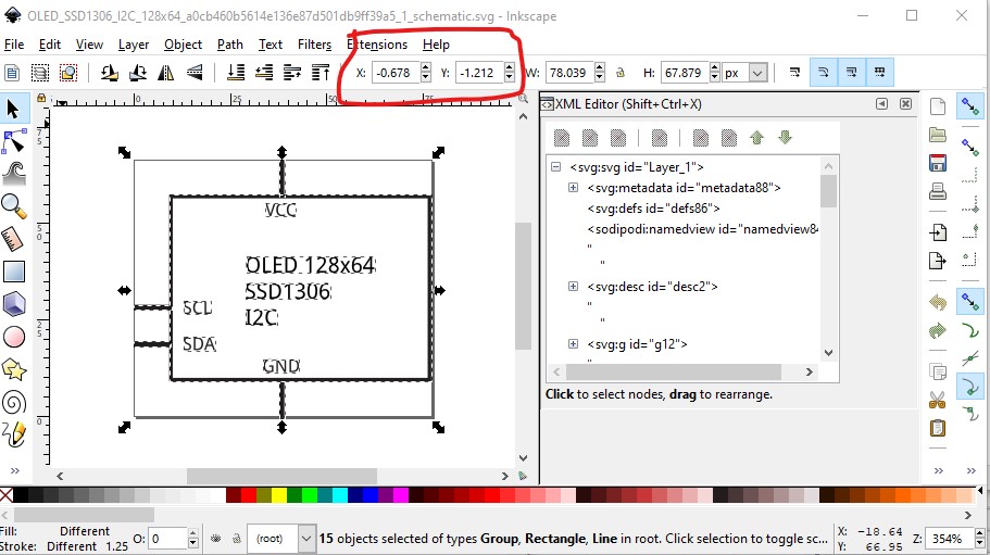
Here we see that the view box is not starting at 0 0 as Fritzing expects. This is the cause of the offset in Y on the pins. To correct this click Edit->select all to select the entire drawing, then Edit->resize page to selection to reset the view box to 0 which produces this
Now with the entire drawing selected click Object->group to create a group of the entire document and name the group schematic like this
Then I duplicated connector2terminal, named the new rectange connector1terminal and moved it .8in up in Y to be at the top of connector1pin.
Now on each pin I changed the style attribute to add a stroke-linecap:round to change the end ot the pin from flat to having a dome so the wire will connect correctly. Then I did an Edit->select all and Edit->Resize page to selection to reset the viewbox to include the entire document (you should always do this at the end of an edit session!) Then I save as plain svg. Now if I reload the part things should work correctly, but they don’t because I was lazy and didn’t ungroup.
The lines have round end caps, but the pins are offset slightly (the red is the pin and it is not on top of the line as it should be) and the pins are still not aligned to the grid. There appears to be something unknown wrong in this svg. Rather than try and figure out what it is, I choose to use the schematic template from here
and make a new svg like this.
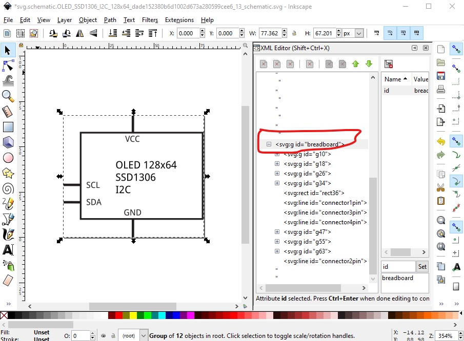
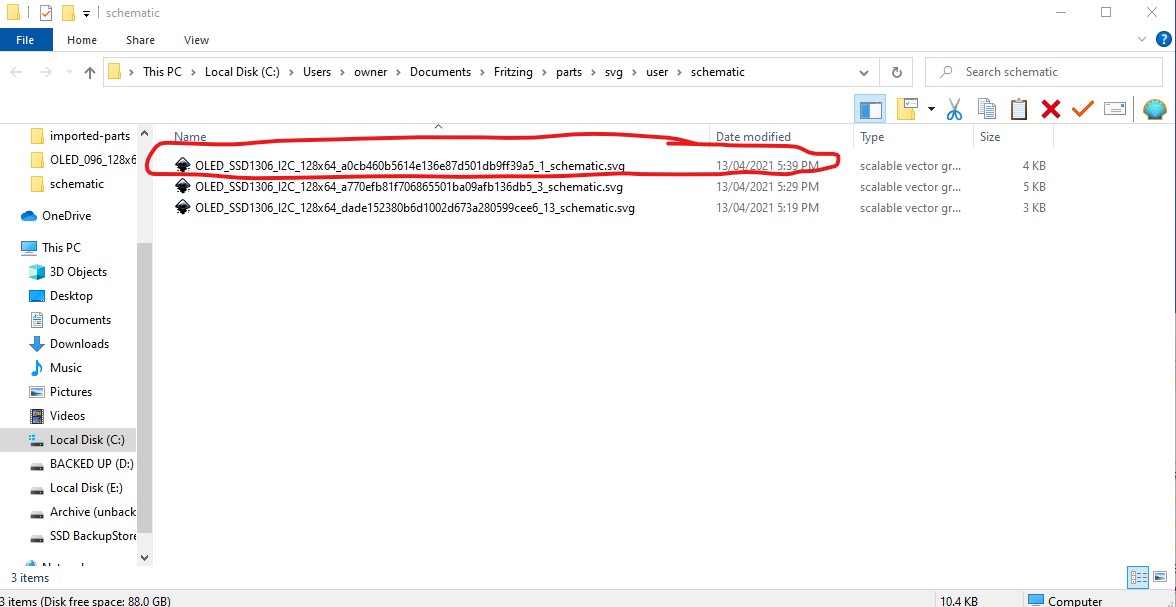
Then I editted the breadboard svg and renamed group g104 to breadboard to create a layerId and saved as plain svg.
then rebuilt the fzpz file which now works. In schematic the pins align to the grid, and the wires connect (without gaps) to the end of the pins as they should
This came from this new part
OLED_096_128x64_I2C_SSD1306.fzpz (7.3 KB)
Peter
2 Likes
Always happy to help people make new parts! We need people willing to contribute to keep Fritzing alive.
Peter
1 Like
What use is that screen shot? It does not add anything useful. There is not information, no download, not reference.
This comment is uncalled for. In my opinion @microMerlin has contributed a lot more that is useful here than you have. I tend to agree that these screen shots without any download reference are not particularly useful. Even with a download reference they are not particularly useful, as a simple google search of the form “fritzing part part-name” as described in the FAQ (whioch I believe @microMerlin wrote) will find most available parts.
edit: In addition I pulled down a handful of files from your archive and ran them through FirtzingCheckPart.py. They come up with errors. It appears these are just copies of parts found on the net with out any error checking or correction. A google search is as useful as this. It would be much more useful if you took the time to check and correct the errors in the parts you post.
File
‘jorgechacblogspot/part.1_7in-tft-lcd_1.fzp’
clean, probably because it is one of my parts and has been through FritzingCheckPart before it was posted.
- Trimpot - 5mm
Error 69: File
‘jorgechacblogspot/svg.breadboard.AG_VR_099833dfe731d65859535de5f31f249e_2_breadboard.svg’
At line 11
Found a drawing element before a layerId (or no layerId)
the lack of a layerId means the part won’t export as an svg.
Error 77: File
‘jorgechacblogspot/svg.icon.AG_VR_099833dfe731d65859535de5f31f249e_2_icon.svg’
At line 16
terminalId connector0terminal can’t be a g as it won’t work.
Error 77: File
‘jorgechacblogspot/svg.icon.AG_VR_099833dfe731d65859535de5f31f249e_2_icon.svg’
At line 17
terminalId connector1terminal can’t be a g as it won’t work.
Error 77: File
‘jorgechacblogspot/svg.icon.AG_VR_099833dfe731d65859535de5f31f249e_2_icon.svg’
At line 18
terminalId connector2terminal can’t be a g as it won’t work.
I don’t believe that it is true this won’t work anymore but it is non the less a bad practice as ungrouping the svg will delete the terminalIds.
Warning 14: File
‘jorgechacblogspot/part.HC-05_b0c1db6c8f5e225ba8413586d9d82be7_7.fzp’
At line 109
terminalId missing in schematicView (likely an error)
Warning 14: File
‘jorgechacblogspot/part.HC-05_b0c1db6c8f5e225ba8413586d9d82be7_7.fzp’
At line 123
terminalId missing in schematicView (likely an error)
Warning 36: File
‘jorgechacblogspot/part.HC-05_b0c1db6c8f5e225ba8413586d9d82be7_7.fzp’
without terminal ids wires will connect in the center of the .1in pin in schematic. The connector numbers also don’t start at zero which will sometimes cause problems with the pin labels being wrong.
Warning 19: File
‘jorgechacblogspot/svg.breadboard.HC-05_e81bbd31de5d521585e93a17a2815bce_4_breadboard.svg’
At line 3
Height 56.691406 is defined in px
in or mm is a better option (px can cause scaling problems!)
Warning 19: File
‘jorgechacblogspot/svg.breadboard.HC-05_e81bbd31de5d521585e93a17a2815bce_4_breadboard.svg’
At line 3
Width 129.33008 is defined in px
in or mm is a better option (px can cause scaling problems!)
With the dimensions in px editing the svg files with an svg editor is a crap shoot. The scale is likely to be wrong in the editor and may or may not be in Fritzing depending on whether Fritzing guesses the scale correctly or not (it often gets it wrong.)
Error 69: File
‘jorgechacblogspot/svg.schematic.HC-05_e81bbd31de5d521585e93a17a2815bce_4_schematic.svg’
At line 17
Found a drawing element before a layerId (or no layerId)
again the part won’t render in an image export file.
Error 17: File
‘jorgechacblogspot/part.HC-05_b0c1db6c8f5e225ba8413586d9d82be7_7.fzp’
No connectors found for view schematicView.
Error 17: File
‘jorgechacblogspot/part.HC-05_b0c1db6c8f5e225ba8413586d9d82be7_7.fzp’
No connectors found for view pcbView.
neither schematic view nor pcb view appear to be functional as they have no connectors defined.
Peter
Guten Abend Peter meine Gewächshaus Steuerung ist Fertig.
sie ist so wie am Anfang…und so bleibt sie auch…ich benötige keine Condensatoren für die Spannung.
Habe da jemanden der Entwickelt Schaltungen der meinte das das der Arduino Abkann er hätte es bis dato noch nie Geschaft einen A/E pin beim Arduino zu Zerstören .
Der FET ist hochohmiger und belastet ihn bei geringer Schaltfrequenz weniger. Wegen Überlastung muss man sich keine sorgen machen. Die Arduino-Ausgänge sind strombegrenzt und praktisch kurzschlusssicher.
also nix für ungut…habe es getestet um Sicher zu gehen das es Klappt
zum Display…
The OLED-128x64-I2C-Monochrome-Display-VDD-GND.fzpz display above should work for this part.
Peter
via google translate
Das obige OLED-128x64-I2C-Monochrome-Display-VDD-GND.fzpz-Display sollte für diesen Teil geeignet sein.
Peter
ist zu klein Peter…
habe das lineal genommen zu messen…