Hi,
I’ve created a new Fritzing part - BME/BMP280 - temperature, humidity, barometric sensor with I2C protocol. Download here: ajcreatif.com/BMP280.fzpz
Thanks for using.
Regards, mtd
Hi,
I’ve created a new Fritzing part - BME/BMP280 - temperature, humidity, barometric sensor with I2C protocol. Download here: ajcreatif.com/BMP280.fzpz
Thanks for using.
Regards, mtd
Not bad, but a few problems:
schematic svg:
is missing the schematic layerId
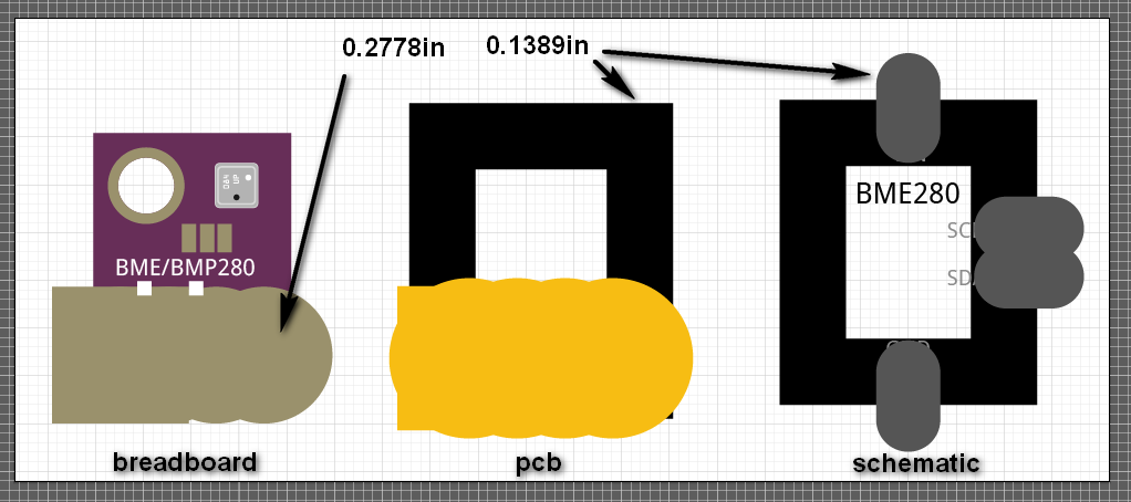
none of the connectorxterminal labels are correct. 0 and 1
are still rect and 2 and 3 are labeled 4 and 5. That causes the wire to terminate in the middle of the pin as shown here:
in the fpz file changed type=“pad” to type=“male”
edit: also changed lablel from BMP280 to M (for module)
The breadboard svg layer ID is bredboard rather than breadboard
Here is a part with these things corrected (and schematic changed slightly to improve readability) and with the scale changed to the standard.
BME280_improved.fzpz (10.1 KB)
Peter
Hi,
thank you for your instructions.
Yes, I’ve obviously missed somethings when creating this part since it is not my routine yet.
I’ve also improved my part and uploaded it to repository mentioned above if someone follows by the link. I hope the part is ok now.
Kindly regards
If these are your first parts you are doing very well. Part creation is a complex process and takes a while to learn, in addition it is poorly documented  meaning asking here for help is pretty much the only way to learn at present. The new parts are mostly fine, but there are several problems. In this part (the bmp280) the fzp file has the schematic layerId as the standard ‘schematic’ but in the schematic svg the layerId is spelled ‘Schematic’ and thus there isn’t a layerId because it doesn’t match (case matters!). This is an error (as opposed to a warning) because it will stop your part from appearing in an export of the sketch to a pdf or other image file. There are a bunch of warning message about various things (such as scale) but they won’t affect the operation of the part. I am using the parts checker available from
(although a not yet released, later version, the github version will complain about less at the moment) to see what problems there are as well as looking at the result in Fritzing. In Fritzing we see there is a problem that the part checker didn’t catch in schematic if you load the part in to fritzing you will see the pins in schematic don’t align to the grid properly. That is likely because the page grid (at least for me on Inkscape 0.92.3) is set to px rather than in. If you reset the grid units to ‘in’ from ‘px’ file->document properties->grids and then adjust the Spacing in x/y from 0.01042 to 0.01 you will see the misalignment. An alternative is to set the tool bar to ‘in’ then check the x/y position of the various pins are all on .1 inch spacing (you need to account for the width of the lines when doing this though). As well the viewbox is slightly wrong. If you select connector1pin the y coordinate is -0.005 in. That means .005 in of the bottom of the pin will be truncated by Fritzing as being beyond the viewbox. The easy way to fix that is to Edit->select all then in document properties->page click Resize page to content to readjust the view box to match the drawing (after realigning the pins!). According to the part check script the 4n25 part is fine, no errors, only a bunch of warnings which won’t affect the operation of the part but the script, lies . It has failed to flag that ‘copper1’ is the layerId in the fzp file but in the pcb svg it is spelled ‘cooper1’ which means the 4n25 part has no top layer pads (the script should have flagged a missing layerId, I’ll have to fix that.) In addition, the pcb hole sizes (from the gerber output drill file Untitled Sketch_drill.txt are incorrect.
T100C0.039685
T101C0.038000
T102C0.039657
The top and bottom values are your parts the middle value (0.038in) is from the .1 headers I used to test the connections. You need to adjust the size of your pads to be 0.038 or a little less (because the typical board house will round up to the next highest drill size making your hole too large). The hole size (in Inkscape, the others are different I think) is pad diameter - (stroke-width * 2). At the usual scale that means pad diameter is .078in and stroke-width is 20 to give a .038 hole. You would need to scale these numbers to match the scale in your drawing.
Peter
Hi, thank you very much for your detail explanations.
The fact is that I didn’t follow tutorial from Fritzing website but I followed other tutorials without paying attention on some details.
The difference I noticed between Illustrator and Inkscape is that if svg file made in Inkscape (XX_improved.fzpz) is imported into Illustrator deform stroke weight so the stroke 0.02in in Inkscape appears as 20px in Illustrator.
For creating pads in pcb file with Illustrator I found that the best way is to make pads as a cyrcle of 0.058in x 0.058in with stroke weight of 0.02in. That appears to be correct - I hope.
Kindly regards
p.s. improved parts uploaded again
Unfortunately the tutorials are mostly a mess. Many of them (other than mine and Old_Grey’s) are for older versions of Fritzing and only somewhat apply any more. I learned to make parts by asking questions here, and am now paying that previous assistance forward ![]() . If we can manage to rekindle interest in Fritzing (by restarting development which I’m slowly working on) maybe we can find someone to improve the tutorials situation.
. If we can manage to rekindle interest in Fritzing (by restarting development which I’m slowly working on) maybe we can find someone to improve the tutorials situation.
That is fairly ugly, but good to know! I may add that to the Inkscape tips page. Is there a way to convert all the stroke widths from px back to in or do you have to change them individually? I haven’t seen any problems with Inkscape reading Illustrator svgs so far. Unfortunately leaving the svgs dimensioned in px is a bad idea. Fritzing tries to guess what the DPI value for px is based on something in the svg and often gets it wrong. So dimensions in in or mm are a far safer bet (as the svg looks fine in the svg editor but is the wrong scale in Fritzing if it guesses wrong). It is preferable to have a scale that makes 1px = 1 thousandth of an inch (although that isn’t consistent even in the core parts so far, one of my projects is to fix that …). I know how to rescale the drawing in Inkscape to get the drawing to the desired scale, but not how to do it in Illustrator. Using the pcb svg from this part as an example, Inkscape sees the scale as 0.75000 when the desirable scale is 10.41667 (why this odd number I’m not sure, but this is what produces the desired result in the view box definition ![]() ). This produces this xml in your svg:
). This produces this xml in your svg:
xmlns=“SVG namespace”
height=“0.541639in”
xml:space=“preserve”
y=“0px”
width=“0.433431in”
x=“0px”
version=“1.1”
viewBox=“0 0 31.207 38.998”
whereas the pcb svg from my BME280_improved part has the desired (as specified in the parts file format document at:
which is a useful reference document!) 1/1000 ratio and looks like this:
xmlns=“SVG namespace”
viewBox=“0 0 427.27806 535.54202”
y=“0px”
height=“0.53554183in”
gorn=“0”
xml:space=“preserve”
version=“1.1”
width=“0.42727792in”
The difference is the ratio of the height/width here is the desired 1/1000 ratio (which sets 1 px to be 1 thousandth of an inch and thus 100 drawing units (after translates which complicate things) is .1 in. Having this ratio makes it possible or the part checking script to check pin spacing on connectors for instance (although it doesn’t yet do that). Worse, some of the parts generated by Fritzing don’t use this scale (I think ICs are one example) if I can get a development environment working again (which is close) I’l make a code change to make generated parts consistent and hopefully fix up those in the parts repository.
Yep that appears to be correct. In Inkscape hole diameter would be 0.078in with a stroke-width of 0.02in and the generated hole is 0.038 (from hole diam - (2 * stroke-width) = hole size). It looks like in Illustrator it is hole diam - stroke width (in inches) which is good to know. Coral Draw has a third way of setting the hole diameter (which is documented in an older forum post somewhere). This part looks fine. This part generates two hole sizes according to the gerber drill.txt file:
T100C0.037972
T101C0.038000
The hole with the square pad is slightly smaller (but the board houses typically round up to the next standard drill size which will be 0.038in).
The check script generates only warnings (which don’t affect the operation of the part.) Usually the layerIds (breadboard, icon, pcb schematic) are groups rather than drawing constructs with labels like this (from the pcb svg):
usual:
<g
id=“copper0”
<g
id=“copper1”
<rect
fill=“none”
…
not usual (and generates a warning):
I don’t know if Fritzing will find the layerId if it isn’t a group and if the layerId is missing the part won’t export as an image (such as a pdf or a png file) but works in all other respects (such as making boards, the gerber export works fine). It is desirable to have the first group in pcb be Silkscreen. If silkscreen is the last group (as in your part) Fritzing tends to select the silkscreen object first (which is rarely what you want) when editing in pcb view in Fritzing.
Peter
Thank you for your patience ![]()
I am attaching an image that show a problem I mentioned about importing Inkscape svgs into Illustrator:
Illustrator also found multiple nasty groups when re-importing previously created svg files in Illustrator by myself. Those groups were created by unknown reason to me only on text layers which refer in text displaced position. To avoid it, it is advisable to keep to a good tutorial ![]()
To change properties of multiple paths in Illustrator the procedure is to select referenced path and then select from menu: Select>Same>Stroke Weight. This will select all paths with the same stroke weight so a new parameter will apply to all of selected paths. But firstly the units should be set form: Edit>Preferences>Units. I hope something helps.
Kindly regards.
That is indeed fairly ugly! It is however fairly obvious that it has happened at least and you have a solution.
One place (there may be more though) where groups are added is when you modify a part with parts editor and save it as a new part. Parts editor often creates large numbers of useless nested groups. I usually ungroup the whole svg as the first step and then regroup it when I’m finished to avoid this.
Peter