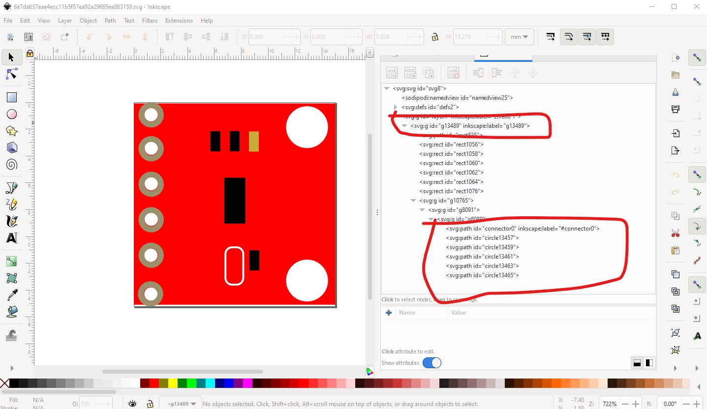
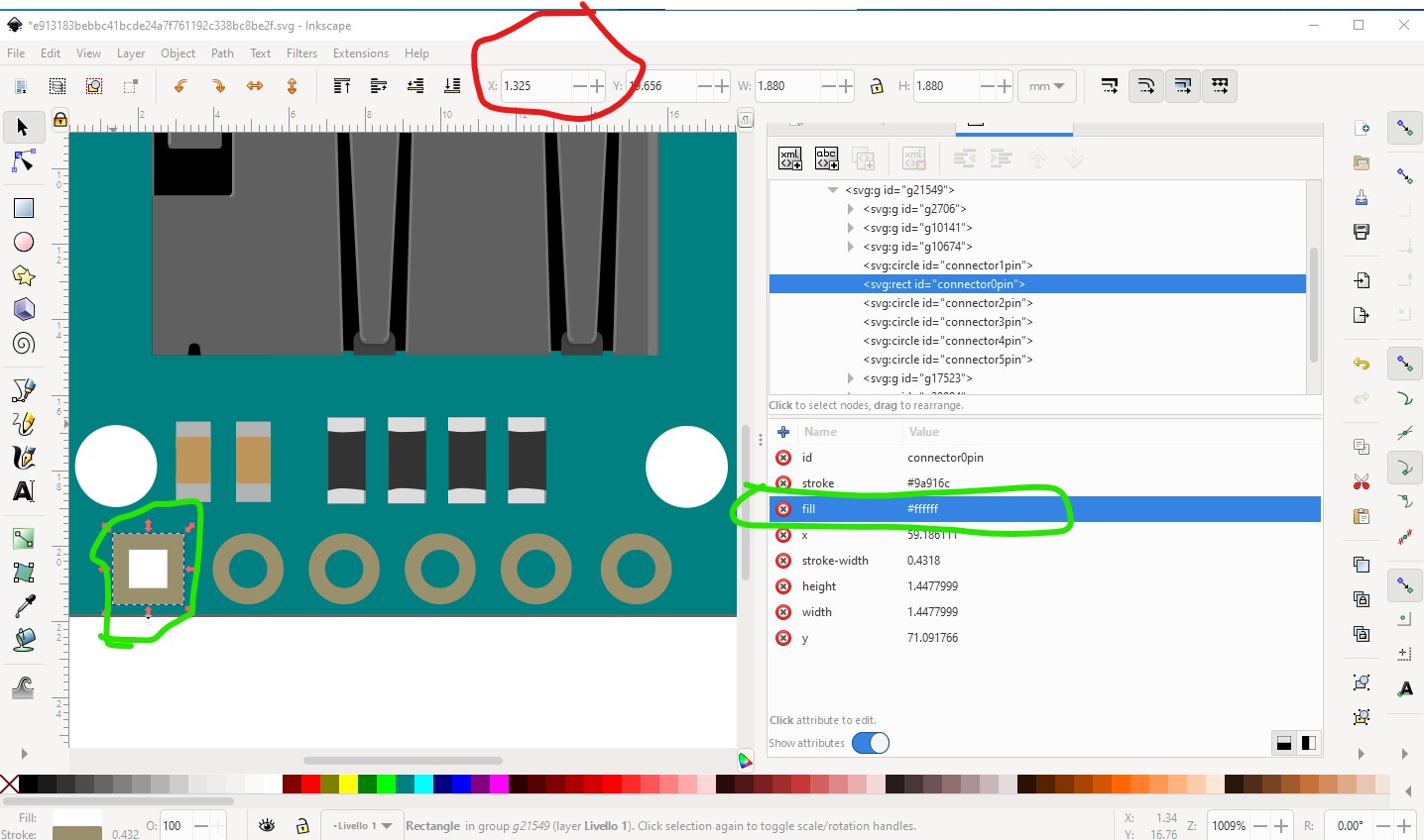
Your svg is misconfigured, as is the fzp file. The svg currently looks like this:
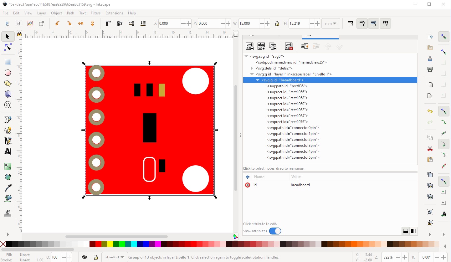
Which is missing the breadboard layerid (the top red circle) and the connector names as set in the fzp file. It should look like this:
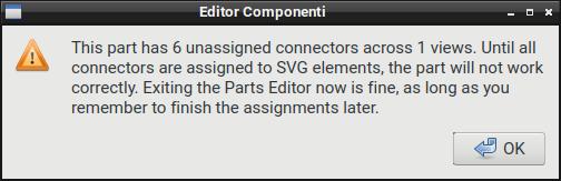
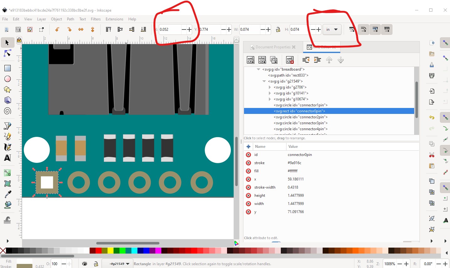
When I I fix xml code inside Inkscape (as shown by the second picture), the six connectors disappear from svg picture 
If you unzip the .fzpz file you will find a file called
part.MCP4725_0b209649dd860fe342f521e54cf50b68_2.fzp
which specifies the names of the layerID (breadboard) and pins (connector0pin - connector5pin) that need to be in the svg.
<breadboardView>
 <layers image="breadboard/MCP4725_0b209649dd860fe342f521e54cf50b68_2_breadboard.svg">
  <layer layerId="breadboard"/>
Fortunately, these lines allready appear inside .fpz file.
and the required pin names in the svg file in the connectors section (the svgId field in this case):
<connector id="connector0" name="pin1" type="male">
 <description>Vout</description>
 <views>
  <breadboardView>
   <p svgId="connector0pin" terminalId="connector0terminal" layer="breadboard"/>
  </breadboardView>
   </layers>
  </breadboardView>
Unfortunately, there are some differences for this block inside .fzp file. My .fzp file appears as the following instead:
<connector id="connector0" name="pin1" type="male">
<description>Vout</description>
<views>
<breadboardView>
<p svgId="connector0pin" terminalId="connector0terminal" layer="breadboard"/>
</breadboardView>
<schematicView>
<p svgId="connector0pin" terminalId="connector0terminal" layer="schematic"/>
</schematicView>
<pcbView>
<p svgId="connector0pin" layer="copper0"/>
<p svgId="connector0pin" layer="copper1"/>
</pcbView>
</views>
</connector>
As well you need to change the family from Generic IC to something else as Generic IC will replace your part with a Generic IC if you change a field in Inspector. Changing the family to MCP4725 is what I would do here.
 <properties>
  <property name="family">MCP4725</property>
  <property name="variant">variant 47</property>
Ok, I’ve fixed this quite easily, thanks.
These tutorials (which applies to the current version of Fritzing) may help as well
I already looked at first two youtube videos from the first link some days ago.