Using transistors on veroboard in the breadboard section

Depends, if Blue’s files work for you they should be fine. The 6 I added are complete parts (all three views are present) where I think only breadboard is present in Blue’s parts. If you only care about breadboard then Blue’s parts may be fine. My parts have new moduleIds and thus will co exist with Blue’s files so you can try both and see which works best for you as well.

Peter

Actually Peter & me made most of the parts. and batch file created by the FZ software.
But, In some case had to edit little bit.

Yes, sorry my bad… The two “Vertical Resistor” parts’ file modue ids named “resistor-vertical” & “resistor200”.
So, as I said, hard to detect the part file…!!

You just can’t drag them into fz documents folder.
You have to rename them also. Like these…

part file:
“part.resistor-vertical.fzp” → “resistor-vertical.fzp”

Svg file:
“svg.breadboard.resistor-vertical_breadboard.svg” → “resistor-vertical_breadboard.svg”
“svg.breadboard.top_diode_300mil.svg” → “top_diode_300mil.svg”
“svg.pcb.top_tantalum_1.svg” → “top_tantalum_1.svg”

Also, svg.breadboard to breadboard folder, svg.pcb to pcb folder… eetc.

If you can do it, then it’s ok… :slightly_smiling_face:

That is not batch file. Unzip it, there will be 21 parts, you have to import them one by one.

(I simply double click it, and it opened by fritzing, In Some PC it doesn’t happens (you have to modify “open with…” in regedit)

OK thanks, there is a lot there for me to work through, can I take a look at it for a few days and get back to you?
Thanks,
Bob.

Hi,
Sorry for the long time away.
I have been using the components you gave me and the picture now looks much more in line with the board I have made, the vertical components look much more realistic.

I have noticed that using veroboard tends to slow my computer down quite a bit? Each move tends to take a second or so?

If I try to resize the veroboard any addition I make ends up with veroboard that has the copper track on both the horizontal and vertical lines which I have to remove manually?

I am also using other components that are ‘side on’ such as tantalum capacitors from the core parts, has anyone made a parts list of these items from above?
see this

I tried to alter the voltage regulator in the power parts of the core section to a vertical but there is much more to it than I can grasp.

I tried going through the parts_editor_help.html
page but it changes tack so often I just kept getting lost.

I am surprised there isn’t a full list of items from above as this is usually how you see a lot of veroboards and pcbs laid out.

The PCB section shows the items clearer so I might try to use that, the problem is that the grid lines are very hard to see, is there any way of making the page look more like veroboard? I have altered the background to white so the components show up better but the grid almost disappears.
Bob.

The way the perf boards are rendered is quite inefficient. I don’t know if there is any intention to change that though.

In Inspector you can choose between perf board (which has a pad for every hole, no strips) or strip board (and then select either horizontal or vertical strips in Inspector. The changing the size of the board should not change what type of board it is.

I think @Blue 's fzbz file is the only collection of top view parts. I’ve made various ones over the years and usually labeled them as top view (so a search in the forums will find them) but not made a list in one place.

I think there is a top view regulator somewhere (I remember making a variety of top view cases 3, 4 and 5 pin versions I think some time back. Part creation is fairly complex. These two sets of tutorials cover the current versions of Fritzing. Many of the others are for older versions (pre parts editor.)

Some people do use pcb view for perfboard projects both because the pcb silkscreen view parts are typically top view and because you can route traces on both the top and bottom of the board (which you can’t in breadboard view.) The grid lines contrast are not currently changeable.
There is an enhancement request open on github
to do this here:

Peter

If I increase the size of the board whilst on strip board it fills the lines in horizontal and vertical. I either have to remove the ones I don’t want individually or go to perfboard and back which removes all the cuts I have made and gives me the strip board renewed in the direction named in the layout box.
delay unit new3.fzz (28.8 KB)
I am trying to get the added file but if i go to breadboard some of the lines are missing and components have been moved, I add them and/or move them and then go to schematic where some of the lines are missing , I add them then go to the breadboard where some of the lines are missing and components have been moved, I add them and on and on?
Can you see what I am doing wrong?
section of new3
if I open the top left the points a and b are not connected as I need them? how can I connect them?

Bob.

I have tried to solve it by using the actual comparator I have, a LM358 but I can’t get it to connect to the veroboard?
delay unit new4.fzz (28.3 KB)
Bob.

Ah! I hadn’t understood that you were trying to preserve cuts. Unfortunately Fritzing regenerates the strip board from scratch (deleting all the cuts) when you resize it so that will happen. The changes are in the routing data base but it would be fairly complex to map that to the new board size. There is some interest in the performance issues around perfboard so it may be worth making an enhancement request on githun here:

to see if there is interest in such an enhancement.

This looks like a bug/feature I have been chasing for the last 5 years or so. If you make changes in another view that are incorrect in some manner, the routing database gets corrupted (the bug/feature part is I’m not sure if this is due to a bug that we can fix, or a non fixable effect of how routing works.) I have about 5 copies of corrupted sketches but have never been able to figure out the sequence of steps that cause the issue to reproduce it so we can try and fix it. What would be very useful (if potentially time consuming!) is if you could do what you did to cause this but keep track of every change in every view (I’m pretty sure what is happening is an incorrect change in schematic gets reflected back in to breadboard causing the error, but have never been able to identify the series of steps that cause the problem.) The usual workaround we recommend is to make all the changes in one view (breadboard, schematic or pcb) and then make only the connections indicated by the rats nest lines in the other two views (so the connections in all three views match the routing data base. ) because once this error occurs the only solution that is known to work is to delete all traces in all views and redo the routing (which can be a lot of work!) The ideal situation would be to reproduce the error so we can see if we can fix it, but as noted I have never been able to reproduce it.

Peter

There is an error on the LM358 in core parts that you used. There is another one that works correctly, so you should use that:

The LM358 on the left has a misalignment in the pins and doesn’t connect to the breadboard. The one on the right does connect correctly.

Peter

“If I increase the size of the board whilst on strip board it fills the lines in horizontal and vertical.”

I fixed this bug a few months ago. The fix is now in 0.9.9. If you are using 0.9.9, it is a bug that we are not aware of. If so, please, open a bug in the bug tracker (GitHub) and upload your file. If not, upgrade to 0.9.9.

If you look at the schematic I added to the last post you will see that a and b are not connected. if you pull a down to b it looks as if they are connected? How can I connect a to b? maybe this is the problem, the schematic looks like two points are connected because the lines run over one another but in fact they arn’t?
delay unit new4.fzz (28.5 KB)

I have changed lm358 for the alternative, see if you can get all the lines to connect in the schematic?

I am in 0.9.3 I have just tried to update but it warns me that updating will lose files in the parts directory, I don’t want to lose all the top down parts I am now using? I also managed to make some relays for the breadboard section I don’t want to lose.
Bob.

In the lastest uploaded fzz file, a and b are electrically connected, but only through the wire to JP1 and back. Simply “crossing” wires in Fritzing (deliveratly) does not make a connection. Moving what “looks” like the join point shows that the wire from JP1 to the 78XX is just passing “under” the joint.

To do what I think you want, create a bend point in wire b. (drag the point away, then back).

Delete the wires from the old join point to JP1 and the op amp (using “Delete wire up to bend points”).

Drag a wire from the op amp to the new bend point.

Finally drag the open end of the “a” wire to the new join point

Now a and b connect at the join/crossing point. However, that does not actually connect to JP1. Moving JP1 shows that a wire that ended at pin 1 is not actually connected.

A little further checking finds that the wire from R11 to JP1 pin 1 is not connected to the wire from a - b.

Fix all of that by dragging the open wire end to the bend point coming from R11

The last bend point in the wire from R11 to JP1 pin 1 is not needed. Double click to delete it.

Then move JP1 back where it came from.

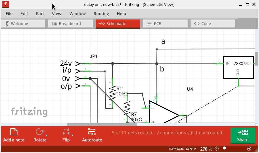
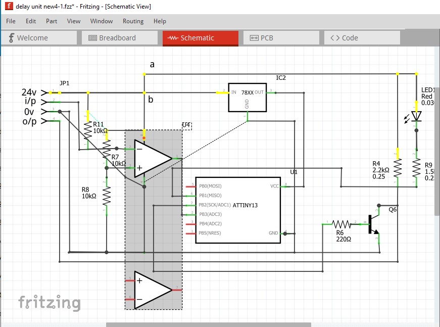
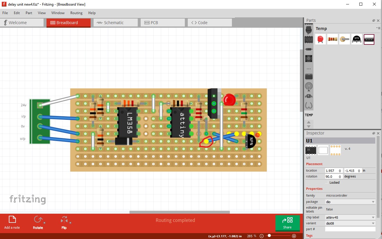
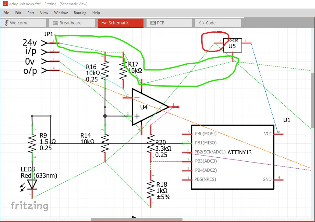
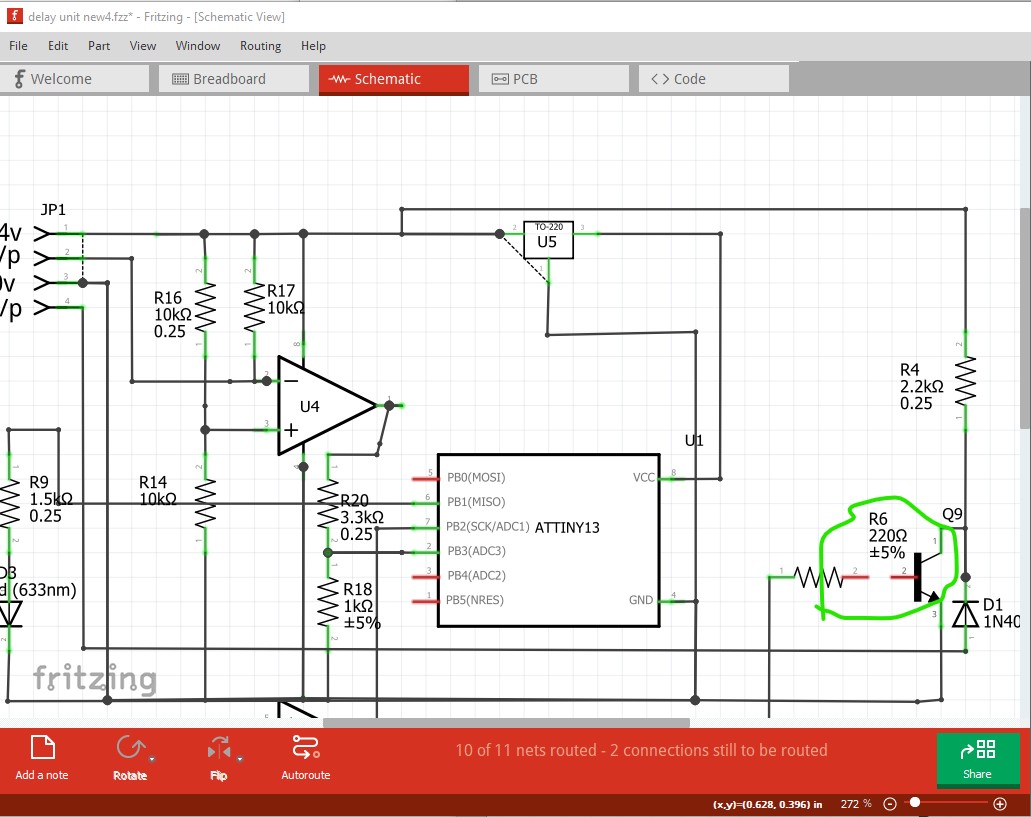
They are in fact connected now. If you right click on any pin all the other pins that connect to it will light yellow:

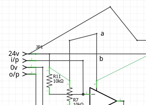
in this case indicating the A is indeed connected to B

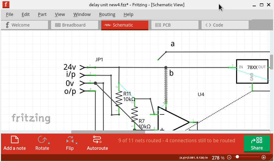
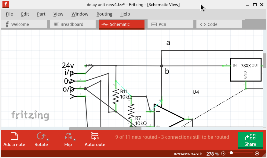
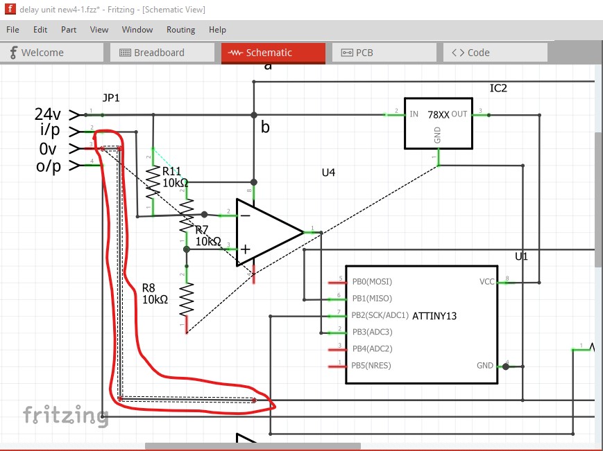
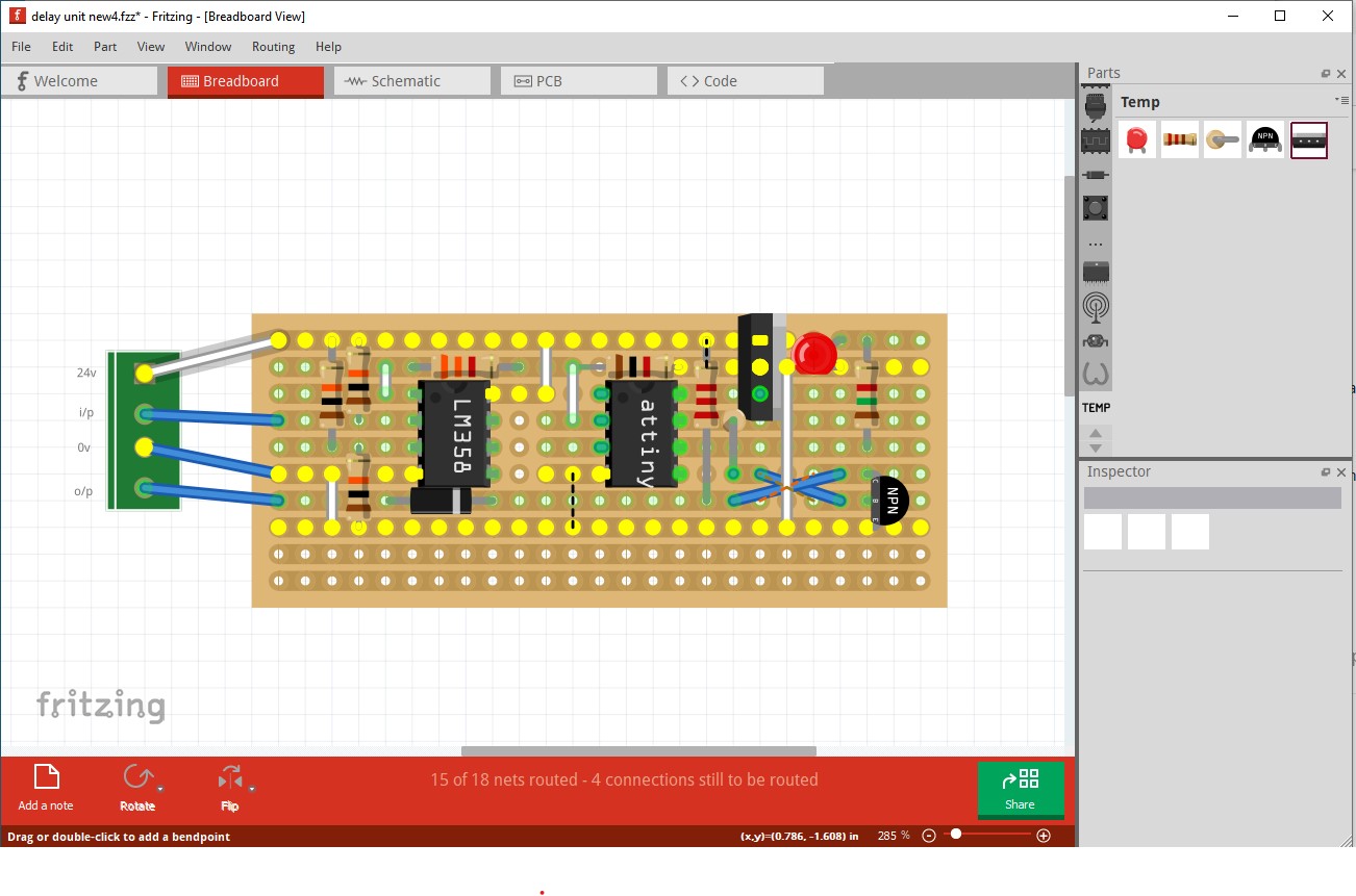
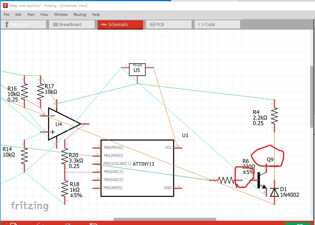
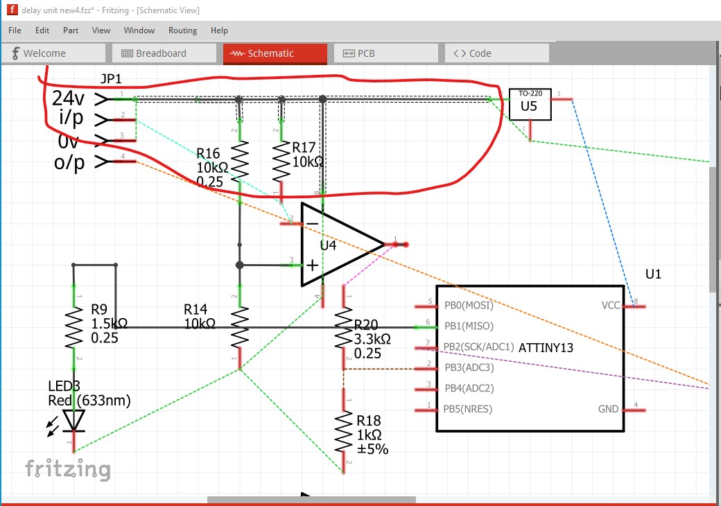
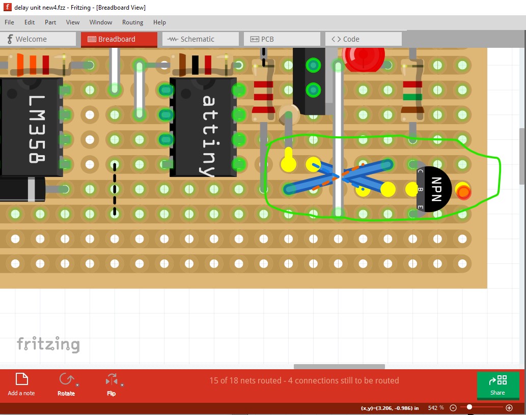
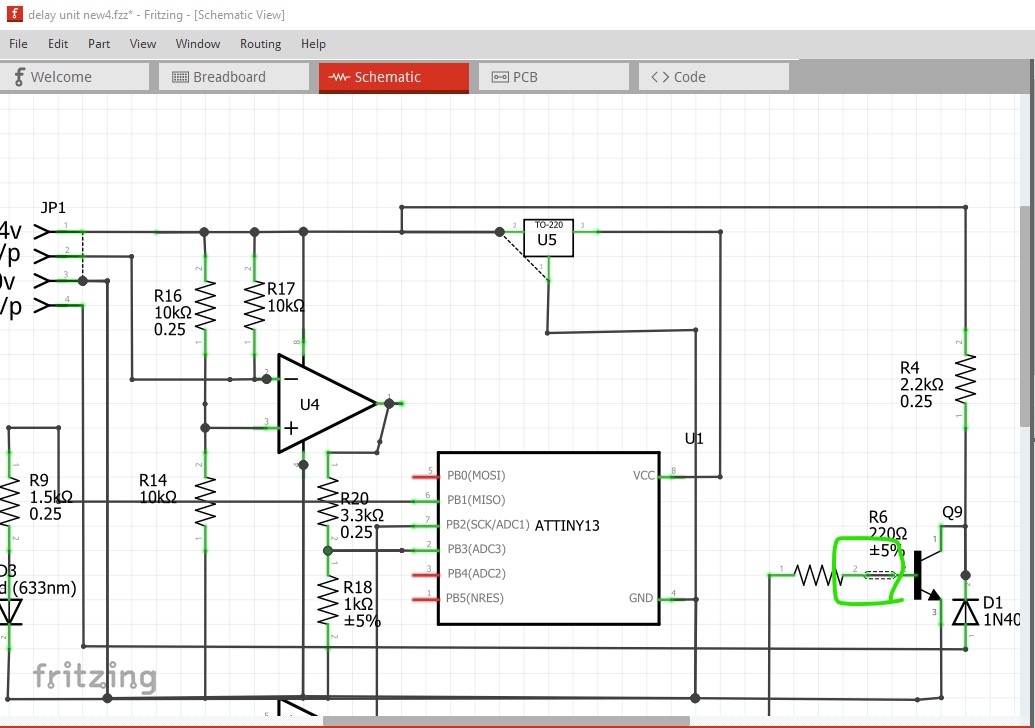
Yes because I have found your problem. You can’t connect a wire to a wire (although it will look like it connects, it isn’t really):

The wire outlined in red is not connected to the rest of that run, it needs to connect to one of the pins such as GND on the ATTINY13 not a wire.

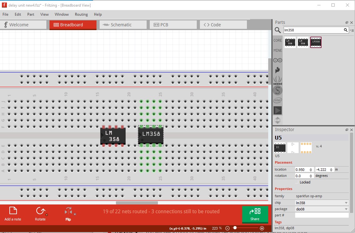
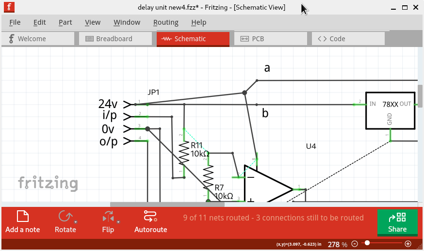
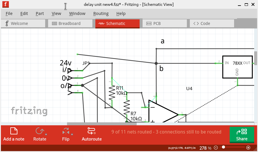
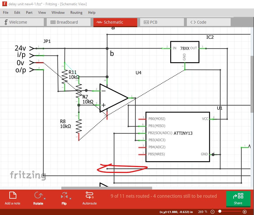
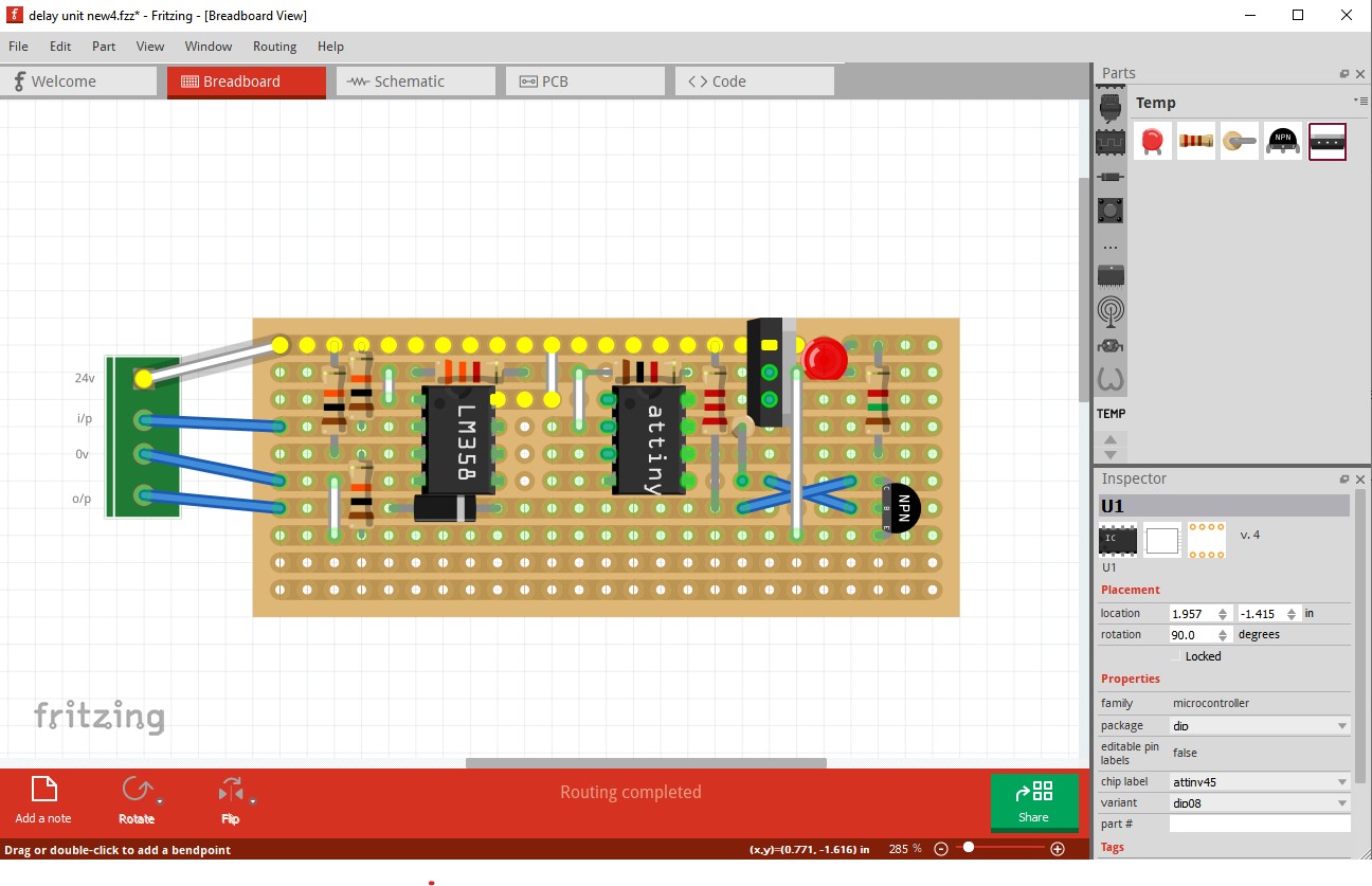
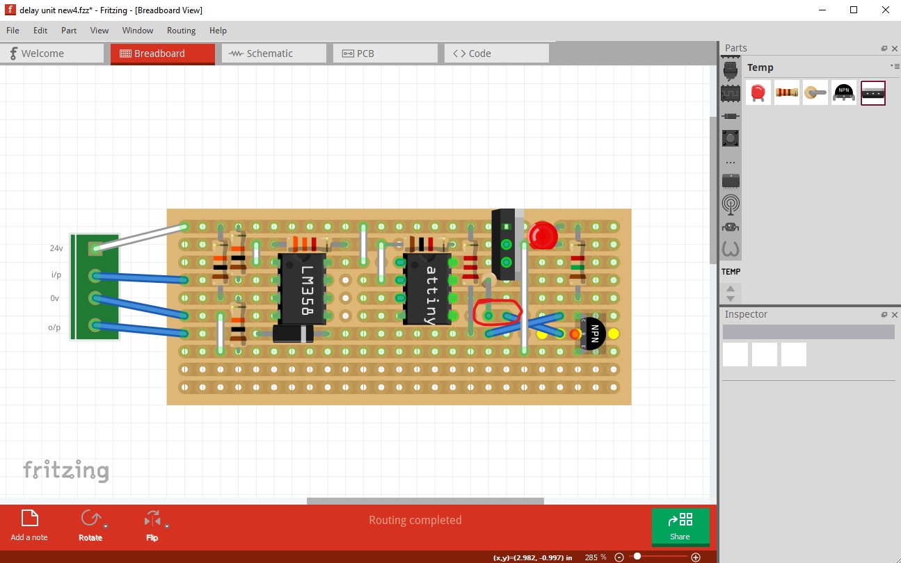
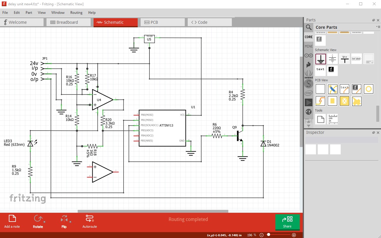
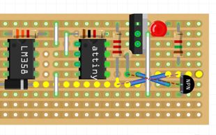
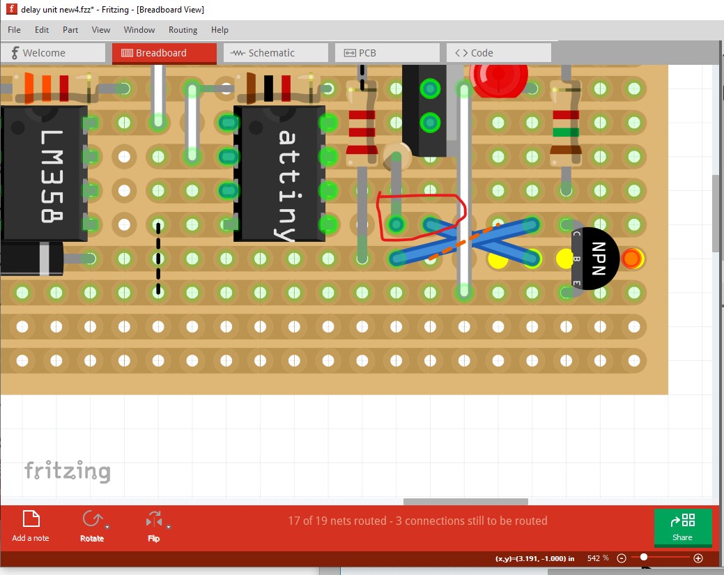
Here I deleted the wire and as we see the wire from the ATTINY13 GND pin just stops in space and doesn’t connect to anything. I then deleted that wire and ran a new wire from the 0V pin to the various ground pins to produce this (I also moved the 358 on to the perf board in Breadboard so Breadboard is complete as well.) That produces this:

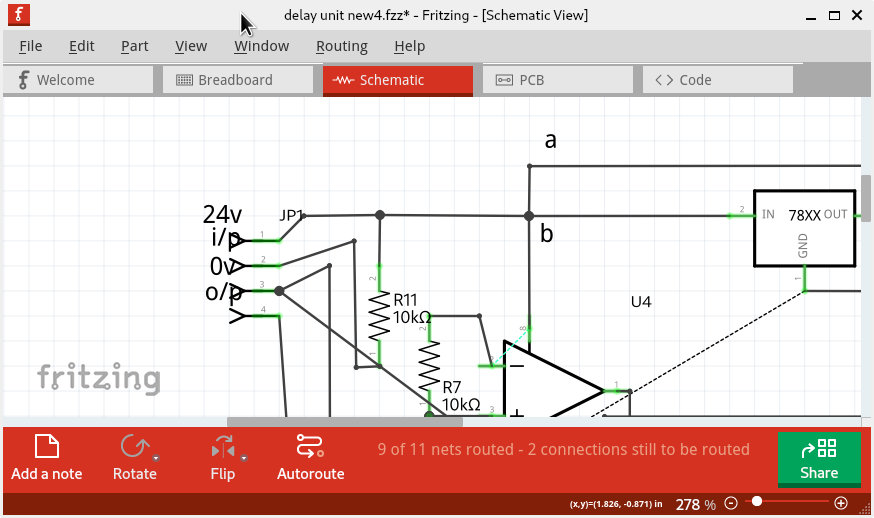
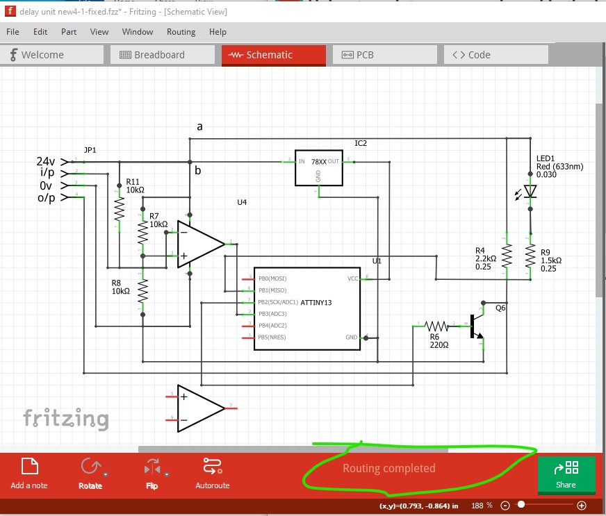
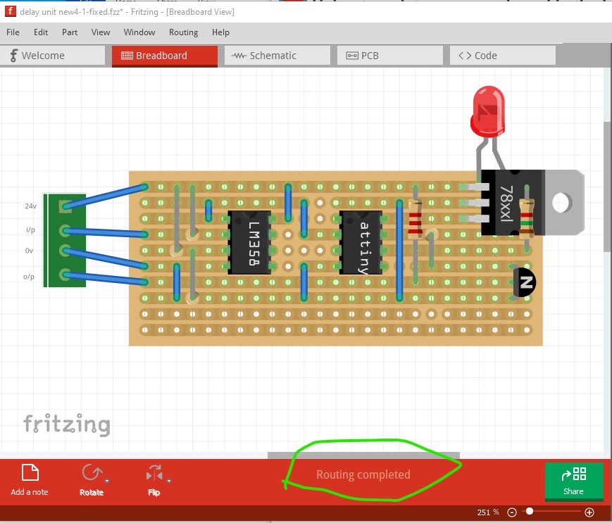
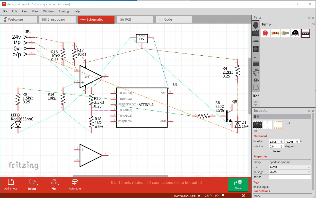
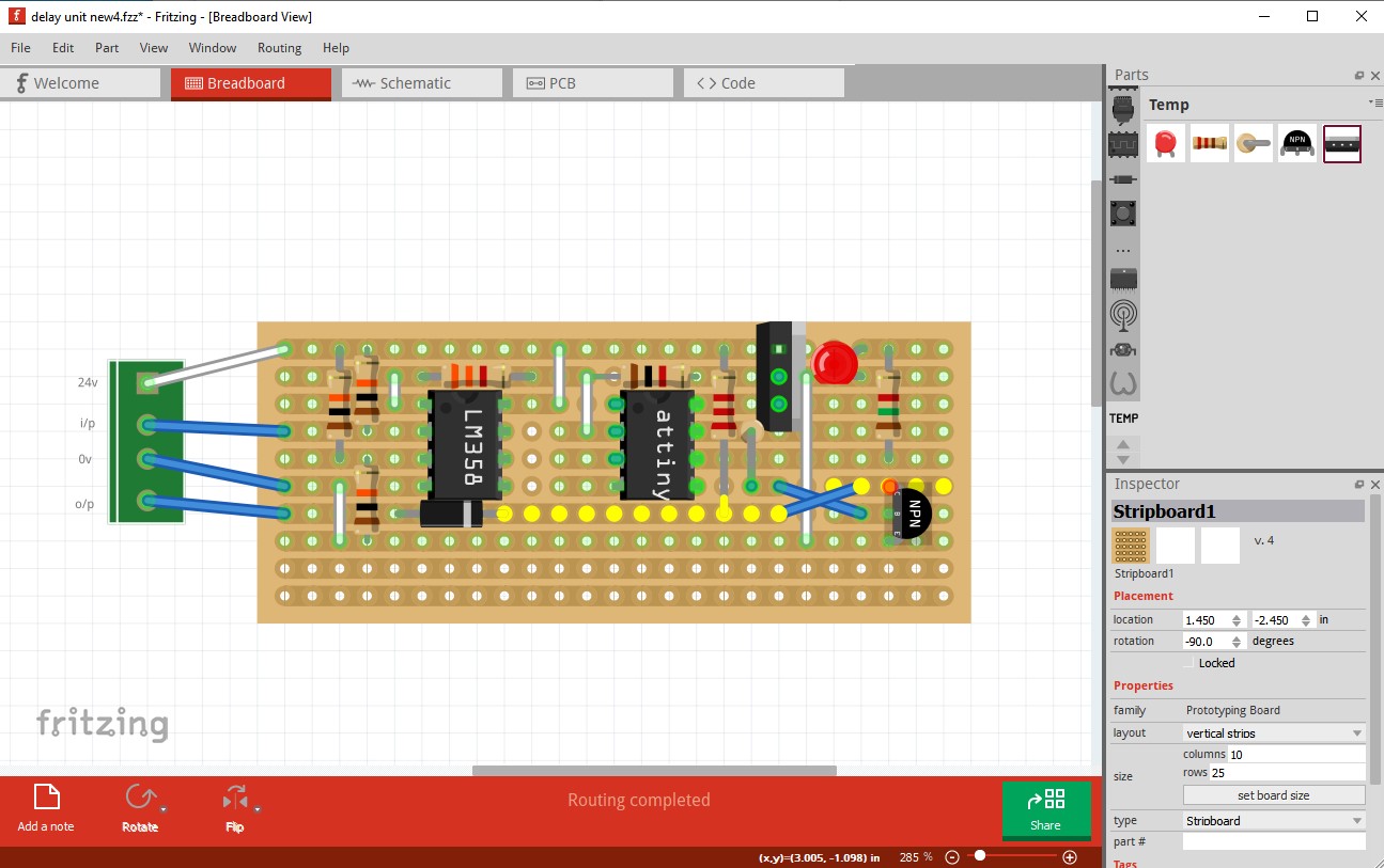
where the routing complete at the bottom indicates there are no longer any non routed connections. Breadboard is the same, routing complete.

they come from this sketch:

delay unit new4-1-fixed.fzz (29.5 KB)

It should not (note the weasel words though) affect any of the parts in the user directories. They are specifically ignored during an upgrade to not delete your custom parts. There are several ways to be sure though, you can make a copy of the user directories which reside here (depending on which operating system you are on)

There are two user directories (with your parts and the parts database) which don’t get touched during an install (to not affect your sketches during upgrades). On Windows they are in

c:\users\username\AppData\Fritzing\roaming\Fritzing (which is a hidden directory so you need to enable hidden directories in explorer) and

c:\Users\username\My Documents\Fritzing (where username is your windows id)

If you don’t have any parts or sketches you want to keep you can just delete those two directories and Fritzing will recreate them, or you can move them aside by renaming them if you want to keep something in them.

linux

~/Documents/Fritzing/parts
~/.config/Fritzing

Mac

/Users/username/Documents/Fritzing/parts
~/.config/Fritzing

In your case you only want to make a copy of the directory to a different file name as a backup. If something bad happens you can shutdown Fritzing then rename the current directories (in case you end up needing something in them) then copy the backup copies in to the Fritzing file names. When Fritzing restarts it will use your old directories. I usually choose to always keep a backup copy of the fzpz files or fzbz files for bins somewhere outside of Fritzing. Then in case of problems I just load the backup copies back in to Fritzing. If Fritzting crashes due to a bug it will sometimes corrupt the user directories and the only solution is to delete them and restore from backups.

Peter

But not where they “appear” to connect.

You ‘can’, connect a wire to a bend point in another wire though.

You can also just drag the open end of the wire to where it is supposed to connect to, then add bend points to route it.

That sparkfun lm358 should really be done using subparts. Some of the problems could be from issues trying to work with bend and join points between the op amps. Which is really ‘over’ instead of between, which makes selection tricky. That does not seem to need any bussed connections, so subparts should have worked before the latest fixes were applied. That is in addition to (apparently) incorrect schematic connector terminals. They exist in the core part fzp and svg, but the wires are connecting to the middle of the connectors, instead of the ends.

Thanks gents, lots of descriptions gone on there.
I have been playing with it in the mean time and managed to get it to work myself but I intend working through your descriptions tomorrow.
I am pleased to see the hints to click on one joint and all the yellow joints are connected to it, that makes it easy. I also didn’t notice the comment in the bottom row about ‘routing completed’, that is also a good indication.
I will continue this tomorrow, you have given me much to think about, thanks for that.
Bob.

Hello again,
I am just about completing the circuit now and have made it.
Thanks to fritzing it was easy to follow the drawing and apart from choosing the wrong TO92 transistor (I need a CBE and not a BCE) the circuit works.
To make it work I added two new blue wires to cross from c to b and b to c and cut both tracks under the links.
Se the enclosed file.
I now have a good looking schematic with a cbe in place but two rats nest wires on the breadboard over the new blue links?
if I put the mouse over a hole at one end it makes all the holes at the other end of the link go yellow, is it connected?
Why do I get the rats nest wires on the breadboard and if I remove them the schematic shows the ic as not connected?
delay unit new4.fzz (47.1 KB)
If I reconnect them on the schematic the rats nest wires are back on the breadboard?
Is this a glitch?
Bob.

There looks to be something wrong with schematic. In breadboard 24V is shorted to ground:

clicking on a ground connection shows a short to the 24V pin. If I then switch to schematic and do Routing->Select all traces then hit the delete key to delete all the traces

breadboard works correctly (indicating there is a short in schematic somewhere)

here ground no longer shorts to 24V indicating that the short was coming from schematic view somewhere. Looking at schematic after deleting all connections indicates there are non connections in breadboard on the base and collector of Q9:

switching to breadboard there is a failed connection in breadboard:

the rest of the trace should also be lighting up yellow when the q9 collector is clicked and it is not indicating there isn’t a connection there. Same with the base, the strip at the base lights but the wire after it does not when it should indicating no connection:

deleting and re running the two wires clears the problem:

with that done schematic routes correctly as well I used a ground net to simplify the wiring:

which produces this sketch

delay unit new4-fixed.fzz (45.8 KB)

Peter

Hello again Peter.
Thank you for the explination.

My schematic shows a retsnest line between the 24v and the 0v in schematic. If I delete it I get all sorts of changes in the breadboard?
The connection between 24v and 0v is interesting? I notice your U5 has the bottom pin connected to the 24v and the left pin to 0v whilst mine is the other way round, I wonder if that is contributing to the 24v/0v connection. I just swapped them over and the connection between 24v and 0v on the breadboard (all the points going yellow) has gone. I automatically assumed it is -left in, bottom common, right out, Most schematics show it that way.
If I click on the hole to the right of the Q9 my schematic shows all the holes on that line, and the holes up to the diode on the next line as yellow indicating they are connected through the blue wire. The same with the centre pin of Q9 (the base) to the resistor going to pin 7 of the attiny indicating both blue lines are connected but my ratsnests are still there?
part of new4

Notice also that the pins down the right side of the attiny are all bright green? I can’t see why this is? If I move it all eight pins are connected with blue wires to the holes on the board.
I like your idea of commoning all the earths it looks so much neater.
Bob.

In this case the U5 part is different, and that is indeed the source of the 24V to ground error:

If I delete the selected wire the rats nest lines indicate that the connection should be the other way

Ground should go to what as you point out is normally the power input pin on the 7805 and 24V should connect to the bottom pin. Connecting the wire the other way in schematic reflects the short between 24V and ground back in to breadboard and pcb (since a connection made in one view propagates to the other views.)

That is because there is a correct connection in schematic (thus showing all the elements of the net connected in breadboard) but the wire in breadboard isn’t connected and thus has a rats nest line as it needs to connect. At this point the wire in schematic is still connected and all the net lights yellow:

then I deleted the wire in schematic:

Now breadboard shows the wire appears to connect the two pads but there is no real connection as the pad after the wire no longer connects without a connection in schematic.

The concept of the nets reflecting from other views takes some getting used to and can cause odd problems like this one.

They are all green because the pins have connected to the pads on the strip board (making a connection between the two and creating a net for each connection.) When you move the IC Fritzing assumes you want to save the existing connections and extends them with wires for you.

Peter