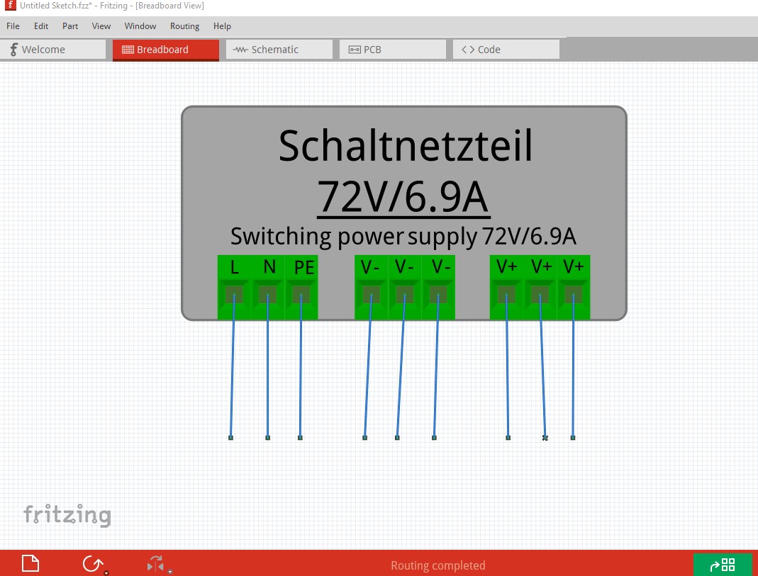
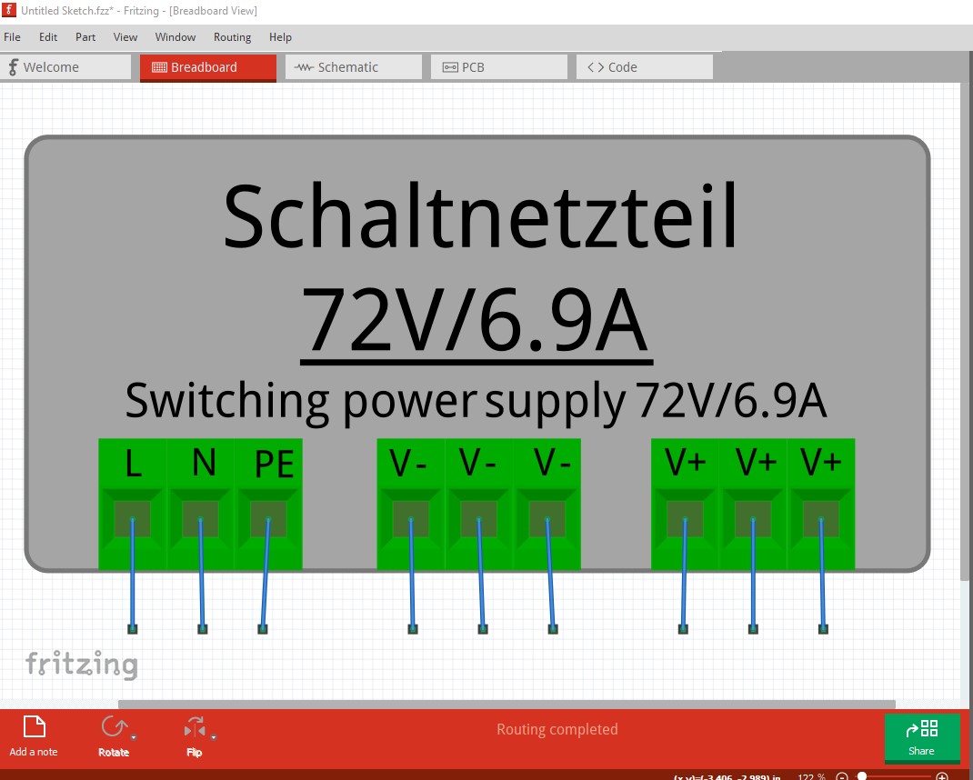
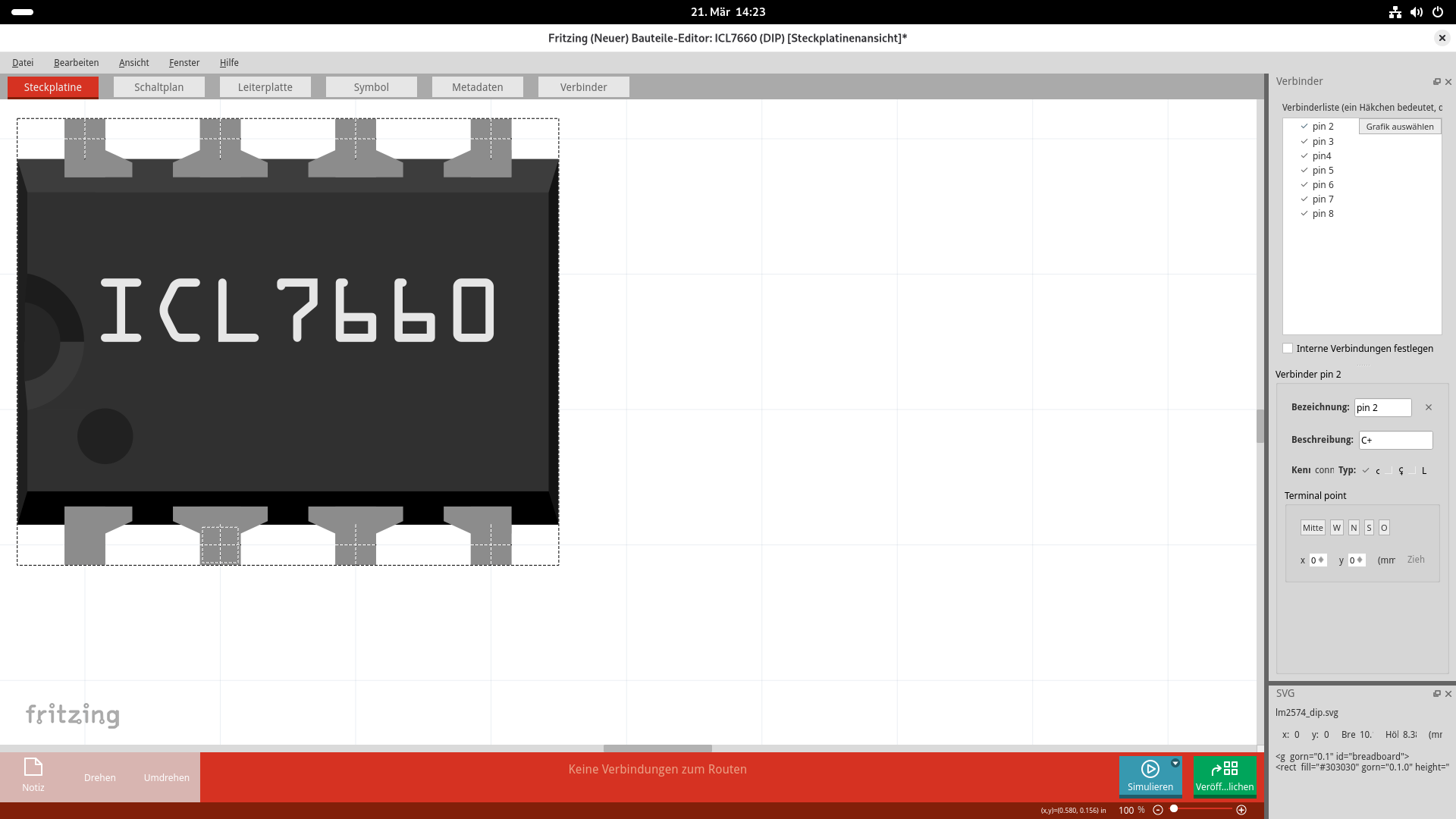
OK, there are a few problems here. Breadboard looks by and large fine
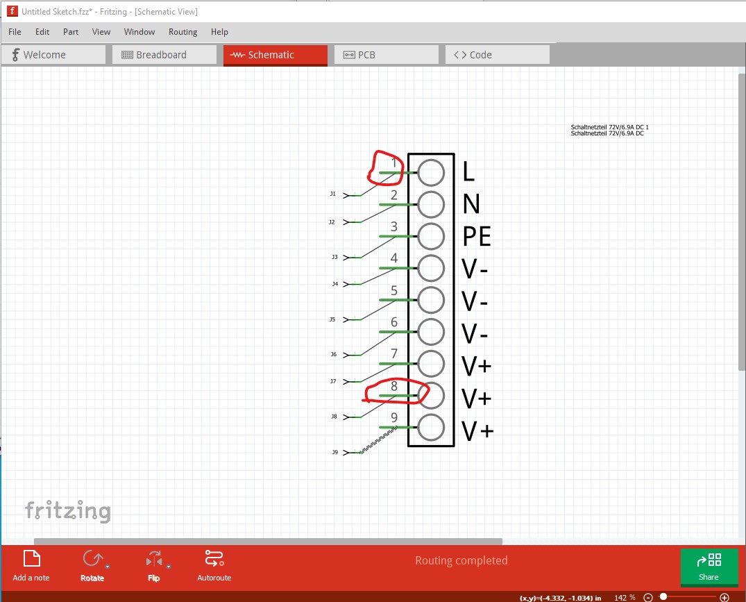
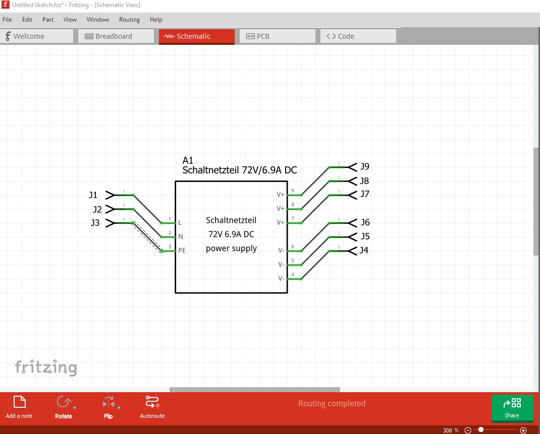
but schematic has a number of problems: it is too large (as small as practical is preferred to provide as much room as possible in schematic). it doesn’t align to the 0.1in grid and the terminals lack terminalIds and thus connect in the middle of the pin rather than the end as they should.
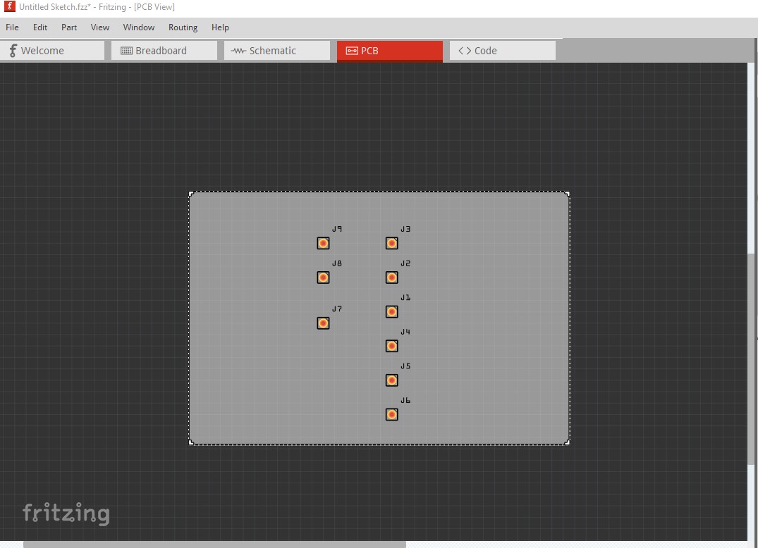
PCB looks fine, except I would suppress it entirely as not useful as the part won’t install in a pcb (how to do that is in my tutorial.)
Then I ran the part through FritzingCheckPart.py which produces the following warnings and errors (this is a development version so won’t exactly match the output from the one available on github!) The output is rather long and only the parts marked Error are important (as generally they will cause Fritzing to break.) The full output is at the bottom of this post. The modified messages are things that FritzingCheckPart corrected (so you know what was changed!) and can usually be ignored. This one should be changed to an Error as it usually (but not always!) as in this case an error.
Warning 14: File
‘part.Schaltnetzteil 72V 6_9A_1e345722911e51301632a08c5ba894a7_7.fzp.bak’
At line 67
terminalId missing in schematicView (likely an error)
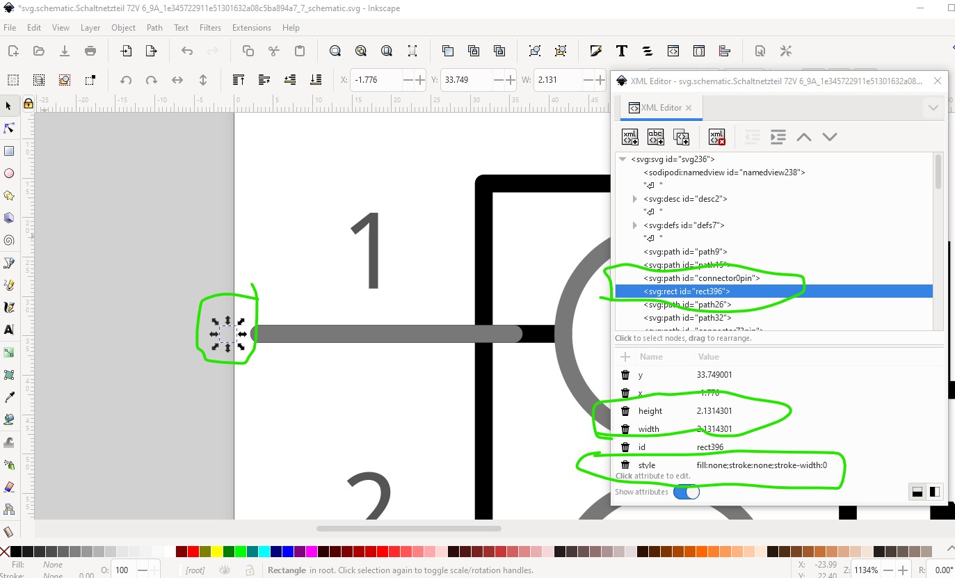
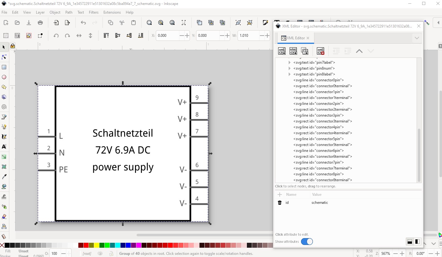
It is why the wire connects in the center of the pin and is corrected like this (in the schematic svg)
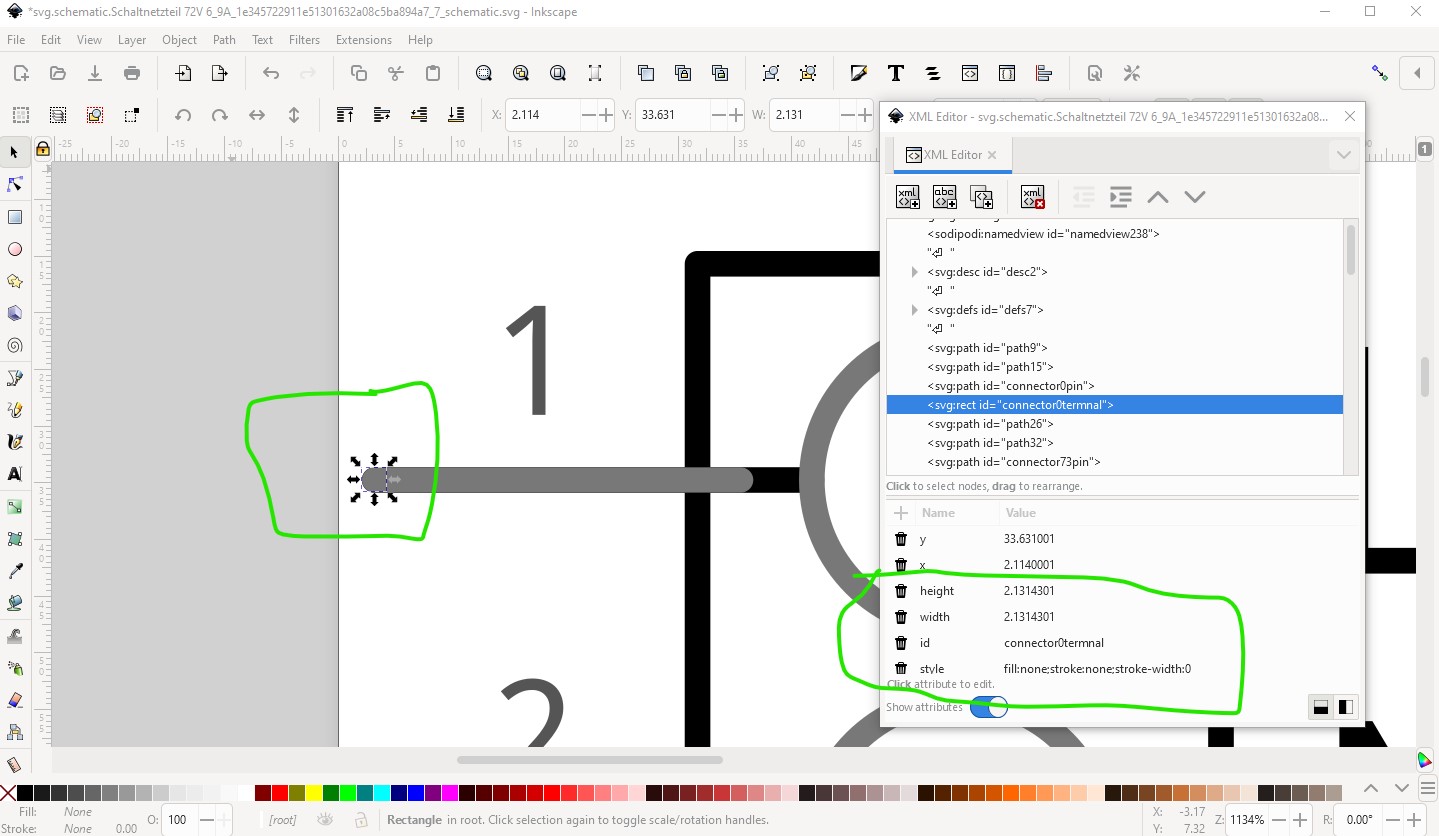
I ungrouped the schematic svg and then created a new rectangle whose height and width are the same as the height of the pin connector0. Now I move that rectangle (square actually!) to the end of connector0 like this and call it connector0terminal
then check that the terminal is defined in the fzp file (which in this case it is) like this
    <connector type="female" name="pin L" id="connector0">
      <description>pin L</description>
      <views>
        <breadboardView>
          <p terminalId="connector0terminal" layer="breadboard" svgId="connector0pin"/>
        </breadboardView>
        <schematicView>
          <p terminalId="connector0terminal" layer="schematic" svgId="connector0pin"/>
        </schematicView>
        <pcbView>
          <p layer="copper0" svgId="connector0pin"/>
          <p layer="copper1" svgId="connector0pin"/>
        </pcbView>
      </views>
    </connector>
note that terminalId=“connector0terminal” exists in the schematic terminal definition so the wire will now connect to the end of the pin rather than the middle. This message too should likely be an error not a warning:
Warning 19: File
‘svg.schematic.Schaltnetzteil 72V 6_9A_1e345722911e51301632a08c5ba894a7_7_schematic.svg.bak’
At line 1
Height 333 is defined in px
in or mm is a better option (px can cause scaling problems!)
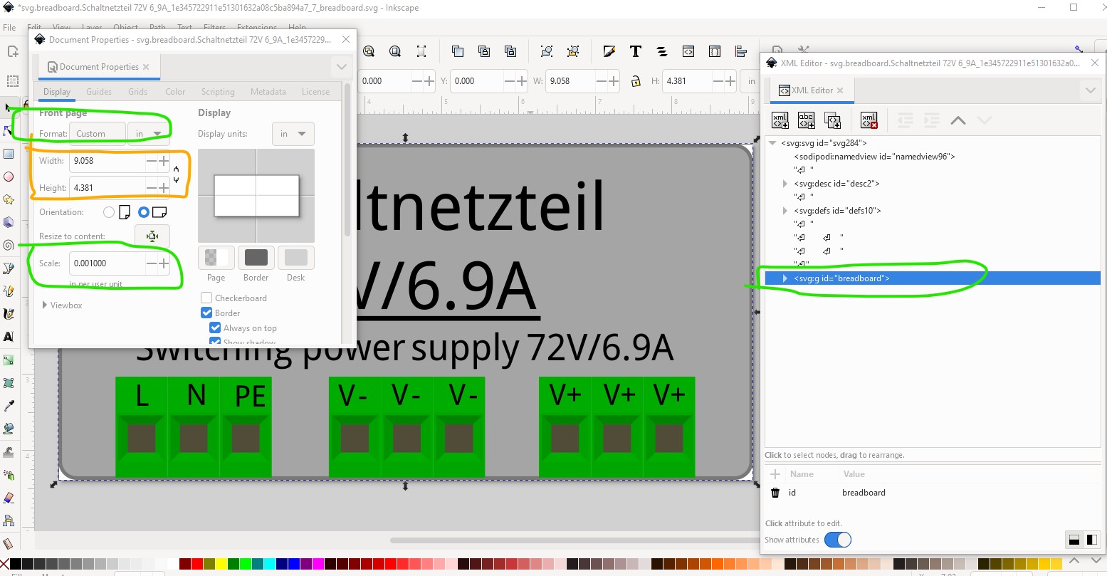
The problem here is that the svg is dimensioned in px rather than in or mm and thus it depends on what DPI value the svg editor is using. Fritzing will typically guess at 72DPI (which was the original and possibly current Illustrator setting.) Inkscape used to be 90DPI (another value Fritzing will use if it thinks the svg is Inkscapes) but current Inkscape uses 96DPI which will then scale wrong. The fix is to change the document in to mm or in (both of which don’t depend on the DPI value) like this and then rescale the drawing.
Changing the dimension to inches also changes the scale (which is desired to be 1 drawing unit = 1/1000in) so I need to change that as well. As well the svg definition doesn’t have a viewbox attribute set so we need to do a Edit–>select all then a Edit->resize page to selection to set a viewbox to end up with this:
where the svg starts at 0 0 in x and y (to be different will cause an offset in Fritzing!) dimensioned in inches with drawing units set to 1/1000 of an inch and the viewbox set to reflect that (by the Edit->resize page to selection.) At this point I still would need to rescale the drawing elements to get them to be the correct size, but in most cases using Randy’s Inkscape extension to create a new (meeting the graphics standards!) schematic will be easier. On to the no layerId messages
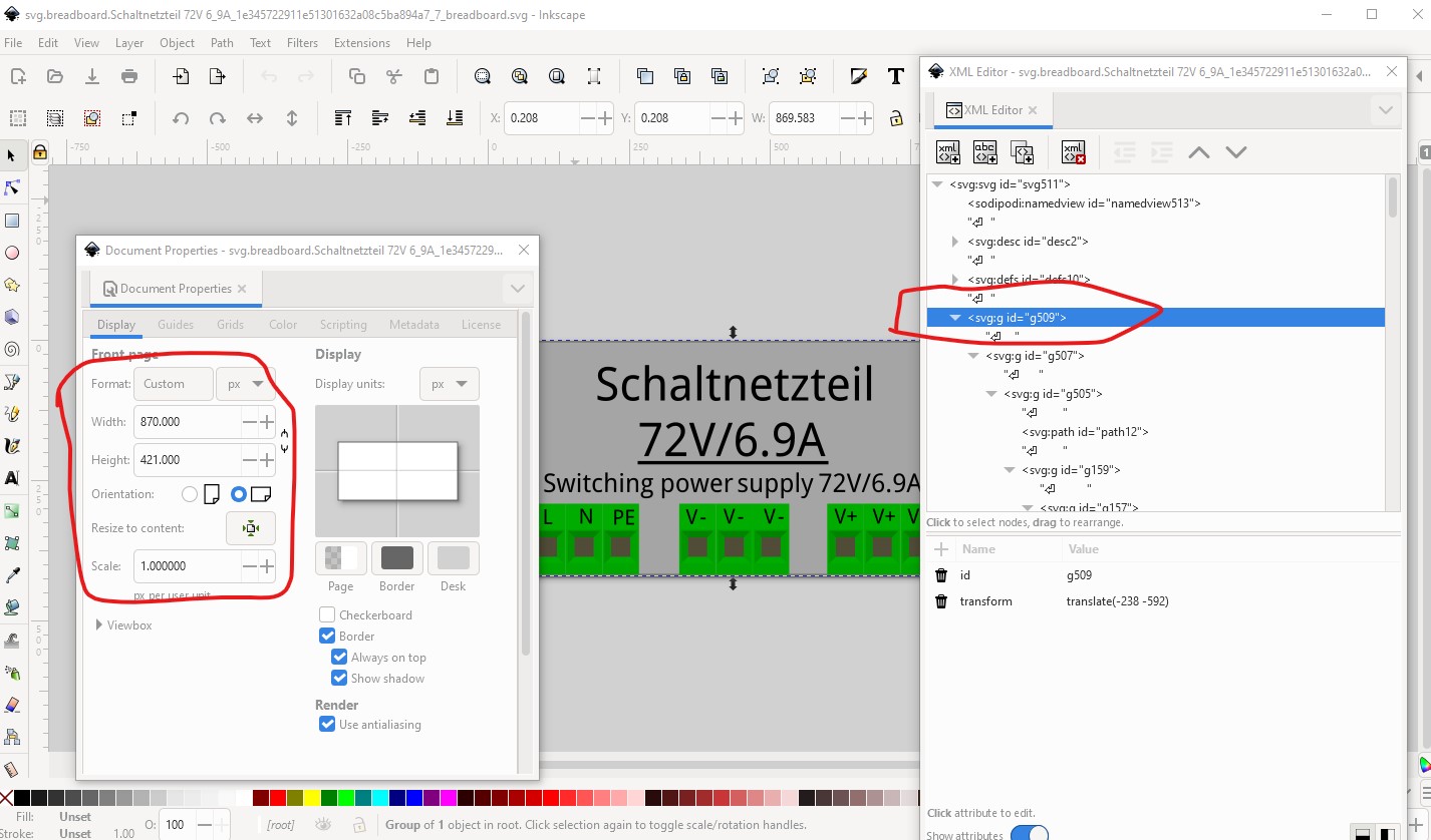
Error 69: File
‘svg.breadboard.Schaltnetzteil 72V 6_9A_1e345722911e51301632a08c5ba894a7_7_breadboard.svg.bak’
At line 16
Found a drawing element before a layerId (or no layerId)
This is indicating that this
has the same incorrect dimension and scale issues as schematic, but also lacks a layerId. In this case group g509 should be changed to “breadboard” to match the breadboard layerId in the fzp file. If the layerId is missing (as in this case) the part will not get exported as an image (jpg, svg, png etc.) which will cause problems. To fix breadboard I rescaled it as is (because I don’t know the real world size circled in orange here of the power supply) and set the layerId like this:
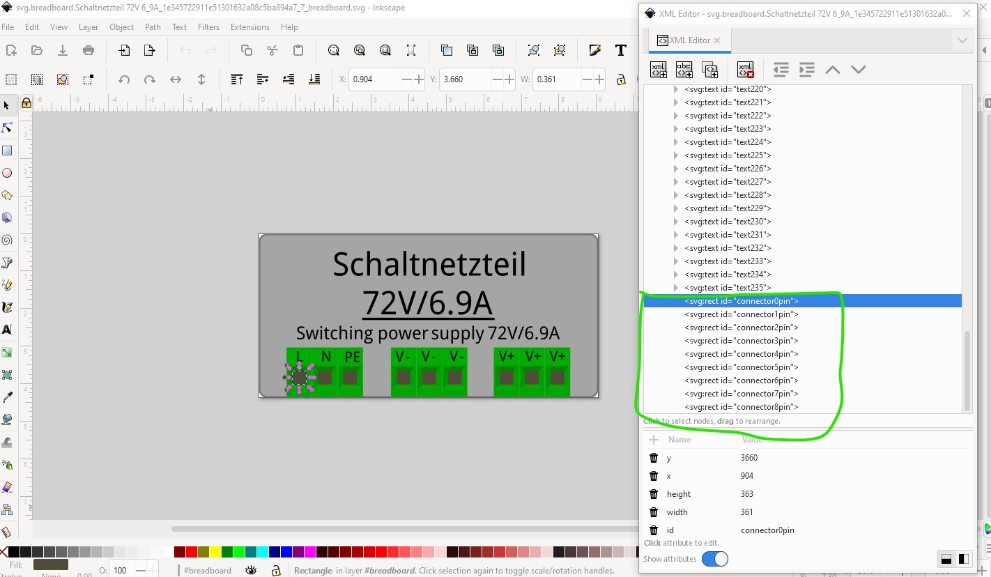
Then I removed the clip paths (which Fritzing doesn’t support) and replaced the connectors with rectangles arranged in order at the bottom of the svg like this. Note there are a bunch of elements listed as “connectorx” that are not really connectors. The script will rename those as well. The first connector is set to be “connector0pin+” so the script know where the first connector is. Then run the script
$ E2fRemoveUnusedConnectors.py ‘svg.breadboard.Schaltnetzteil 72V 6_9A_1e345722911e51301632a08c5ba894a7_7_breadboard.svg’
*** Process svg.breadboard.Schaltnetzteil 72V 6_9A_1e345722911e51301632a08c5ba894a7_7_breadboard.svg ***
line 42 connector ‘connector3pin’ deleted as unused.
line 46 connector ‘connector6pin’ deleted as unused.
line 50 connector ‘connector9pin’ deleted as unused.
line 54 connector ‘connector12pin’ deleted as unused.
line 58 connector ‘connector15pin’ deleted as unused.
line 62 connector ‘connector18pin’ deleted as unused.
line 66 connector ‘connector21pin’ deleted as unused.
line 70 connector ‘connector27pin’ deleted as unused.
line 74 connector ‘connector30pin’ deleted as unused.
line 78 connector ‘connector33pin’ deleted as unused.
line 82 connector ‘connector36pin’ deleted as unused.
line 86 connector ‘connector39pin’ deleted as unused.
line 90 connector ‘connector42pin’ deleted as unused.
line 94 connector ‘connector45pin’ deleted as unused.
line 98 connector ‘connector51pin’ deleted as unused.
line 102 connector ‘connector54pin’ deleted as unused.
line 106 connector ‘connector57pin’ deleted as unused.
line 110 connector ‘connector60pin’ deleted as unused.
line 114 connector ‘connector66pin’ deleted as unused.
line 118 connector ‘connector69pin’ deleted as unused.
line 122 connector ‘connector72pin’ deleted as unused.
line 126 connector ‘connector78pin’ deleted as unused.
line 130 connector ‘connector81pin’ deleted as unused.
line 134 connector ‘connector84pin’ deleted as unused.
line 138 connector ‘connector87pin’ deleted as unused.
line 142 connector ‘connector90pin’ deleted as unused.
line 146 connector ‘connector93pin’ deleted as unused.
line 150 connector ‘connector96pin’ deleted as unused.
line 154 connector ‘connector102pin’ deleted as unused.
line 158 connector ‘connector105pin’ deleted as unused.
line 162 connector ‘connector108pin’ deleted as unused.
line 166 connector ‘connector111pin’ deleted as unused.
line 170 connector ‘connector114pin’ deleted as unused.
line 174 connector ‘connector117pin’ deleted as unused.
line 178 connector ‘connector120pin’ deleted as unused.
line 182 connector ‘connector126pin’ deleted as unused.
line 186 connector ‘connector129pin’ deleted as unused.
line 190 connector ‘connector132pin’ deleted as unused.
line 194 connector ‘connector135pin’ deleted as unused.
line 198 connector ‘connector141pin’ deleted as unused.
line 202 connector ‘connector144pin’ deleted as unused.
line 206 connector ‘connector147pin’ deleted as unused.
line 210 connector ‘connector153pin’ deleted as unused.
line 214 connector ‘connector156pin’ deleted as unused.
line 218 connector ‘connector159pin’ deleted as unused.
line 222 connector ‘connector162pin’ deleted as unused.
line 226 connector ‘connector165pin’ deleted as unused.
line 230 connector ‘connector168pin’ deleted as unused.
line 234 connector ‘connector171pin’ deleted as unused.
line 238 connector ‘connector177pin’ deleted as unused.
line 242 connector ‘connector180pin’ deleted as unused.
line 246 connector ‘connector183pin’ deleted as unused.
line 250 connector ‘connector186pin’ deleted as unused.
line 254 connector ‘connector189pin’ deleted as unused.
line 258 connector ‘connector192pin’ deleted as unused.
line 262 connector ‘connector195pin’ deleted as unused.
line 266 connector ‘connector201pin’ deleted as unused.
line 270 connector ‘connector204pin’ deleted as unused.
line 274 connector ‘connector207pin’ deleted as unused.
line 278 connector ‘connector210pin’ deleted as unused.
line 282 connector ‘connector214pin’ deleted as unused.
line 287 connector ‘connector215pin’ deleted as unused.
line 291 connector ‘connector216pin’ deleted as unused.
line 295 connector ‘connector220pin’ deleted as unused.
line 300 connector ‘connector221pin’ deleted as unused.
line 305 connector ‘connector222pin’ deleted as unused.
line 310 connector ‘connector223pin’ deleted as unused.
line 315 connector ‘connector224pin’ deleted as unused.
line 320 connector ‘connector225pin’ deleted as unused.
line 325 connector ‘connector226pin’ deleted as unused.
line 330 connector ‘connector227pin’ deleted as unused.
line 335 connector ‘connector228pin’ deleted as unused.
line 340 connector ‘connector229pin’ deleted as unused.
line 345 connector ‘connector230pin’ deleted as unused.
line 350 connector ‘connector231pin’ deleted as unused.
line 355 connector ‘connector232pin’ deleted as unused.
line 360 connector ‘connector233pin’ deleted as unused.
line 365 connector ‘connector234pin’ deleted as unused.
line 370 connector ‘connector235pin’ deleted as unused.
line 376 connector ‘connector0pin+’ changed to ‘connector0pin’.
line 382 connector ‘rect310’ changed to ‘connector1pin’.
line 388 connector ‘rect312’ changed to ‘connector2pin’.
line 394 connector ‘rect314’ changed to ‘connector3pin’.
line 400 connector ‘rect316’ changed to ‘connector4pin’.
line 406 connector ‘rect346’ changed to ‘connector5pin’.
line 412 connector ‘rect348’ changed to ‘connector6pin’.
line 418 connector ‘rect350’ changed to ‘connector7pin’.
line 424 connector ‘rect352’ changed to ‘connector8pin’.
which produces this svg:
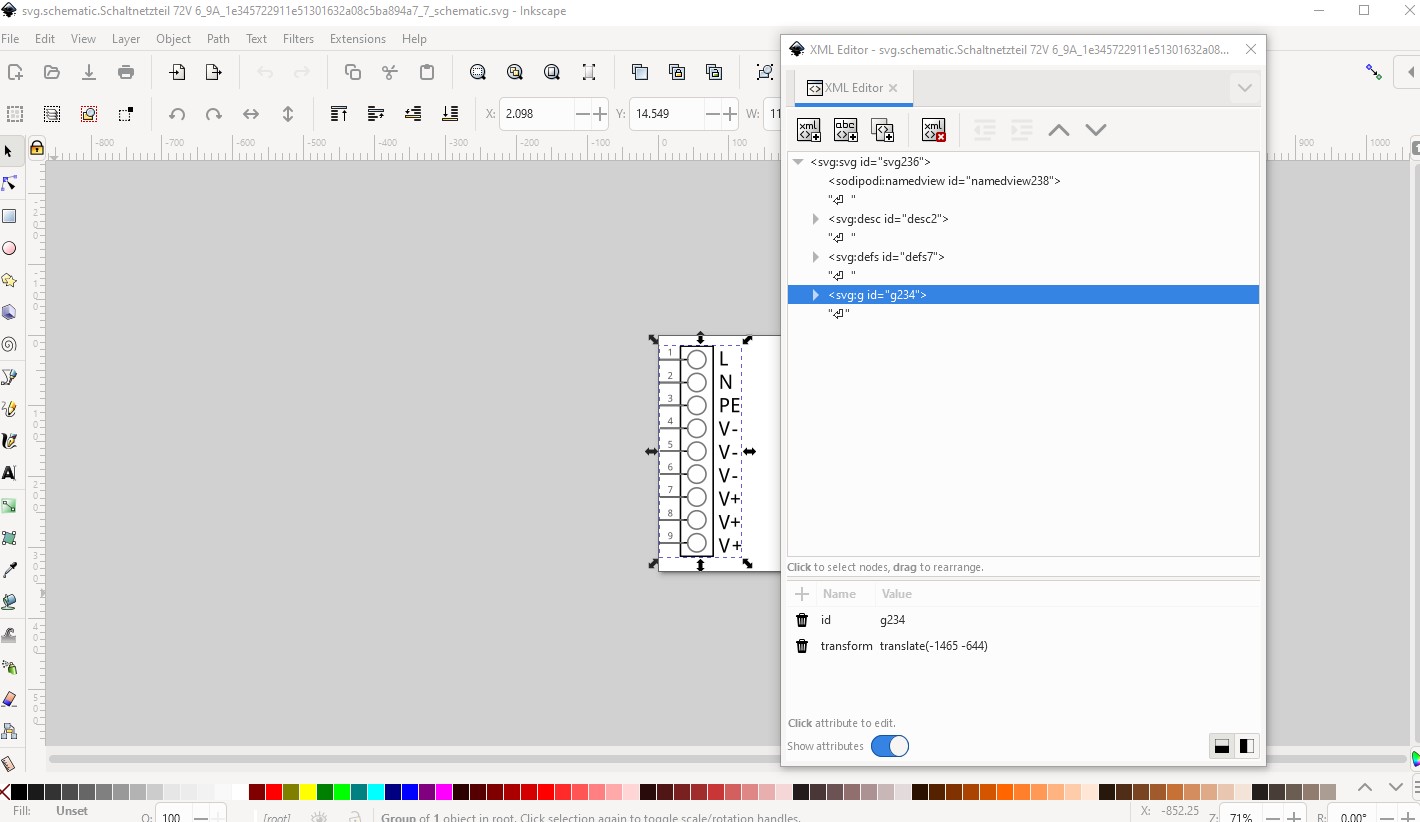
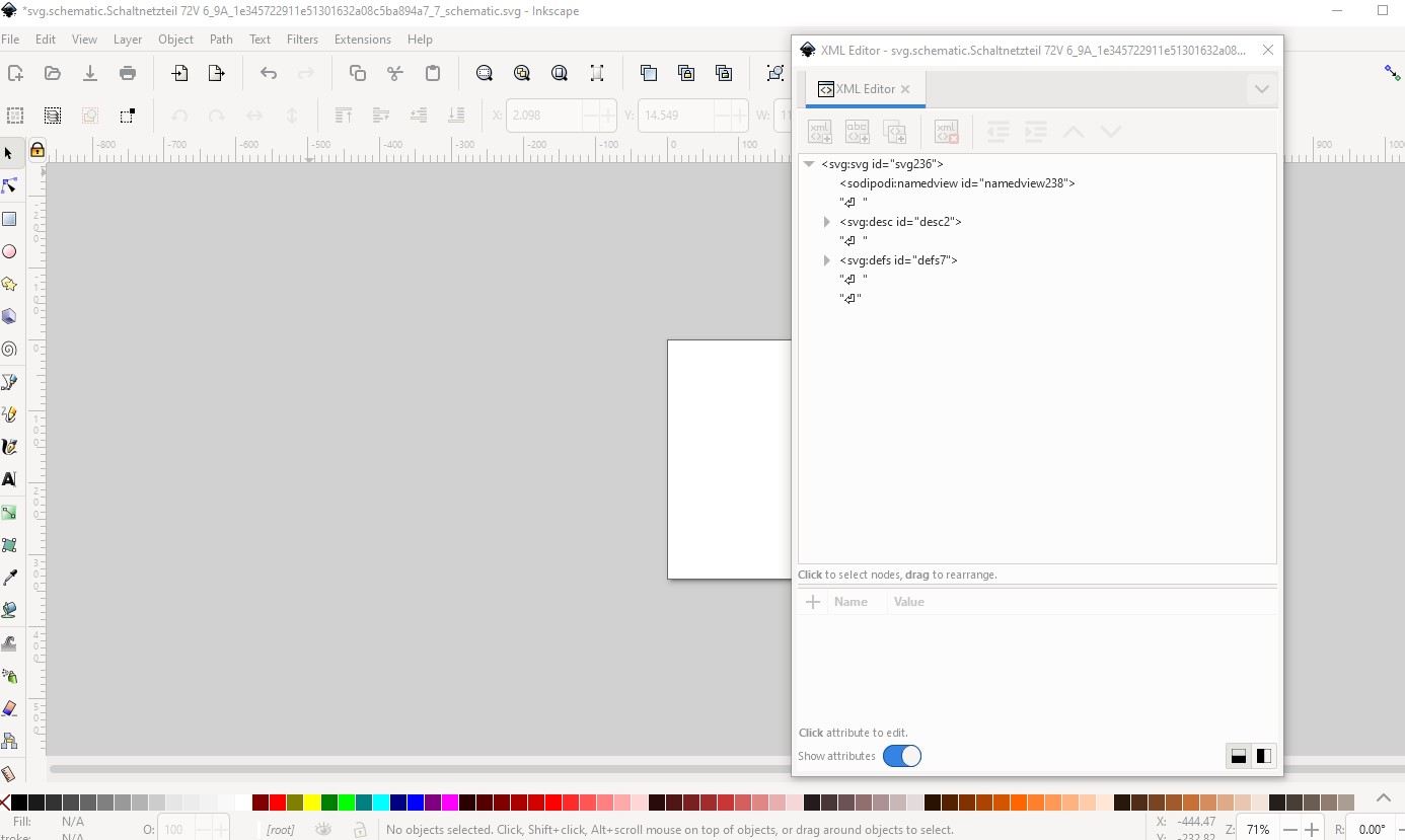
with only the active pins listed in order at the bottom of the svg. The elements that used to have the name connectorxx have changed to element type (i.e. text) from connector. So now breadboard is ready to be saved as plain svg. On to schematic. As noted Randy’s Inkscape extension is the easiest way to make a schematic. Start by deleting the old schematic.
which leaves this
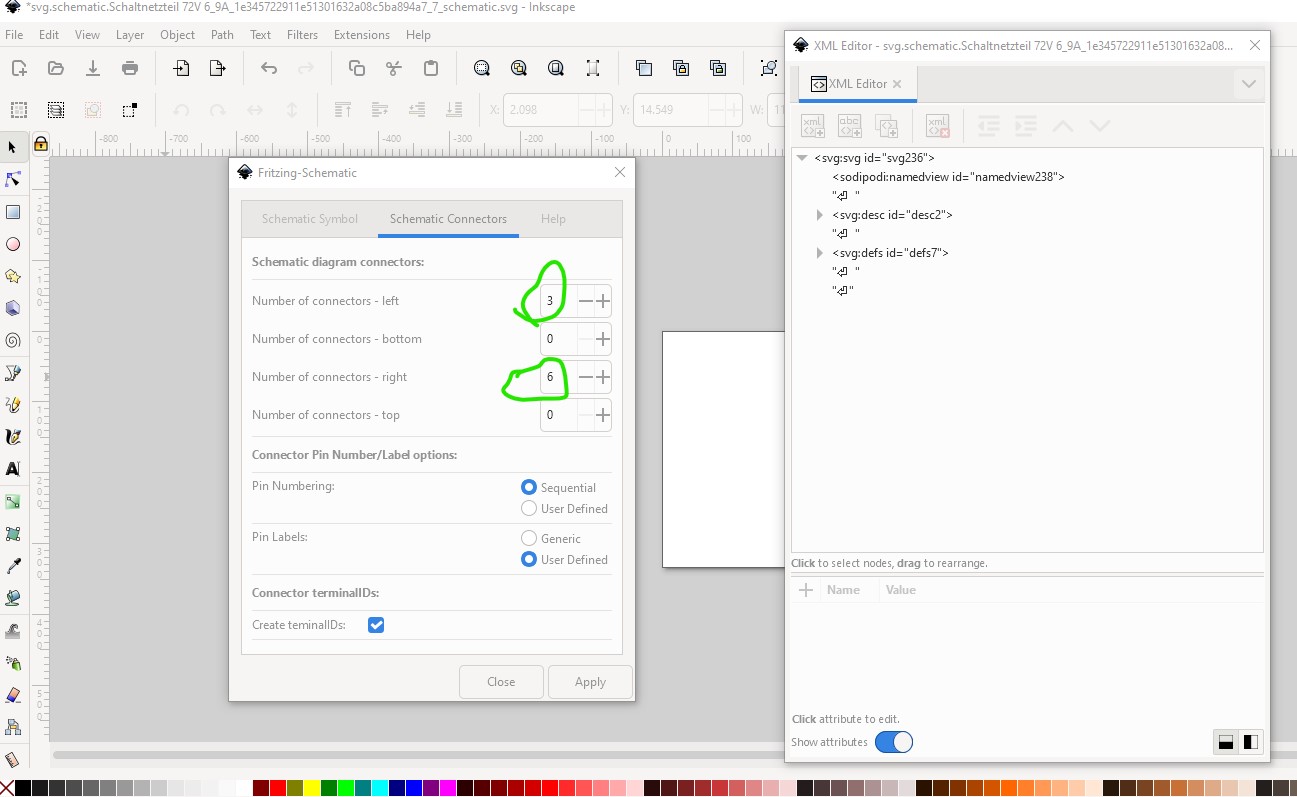
so start the extension and set the parameters
We need 3 connectors on the left and 6 on the right (which needs 0.7in in height) so set the size to 0.8 x 0.8in. Set the title. Then move on to the connections
set 3 left and 6 right then apply.
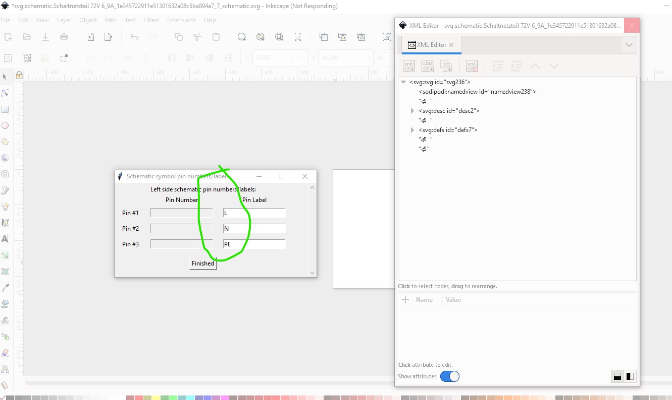
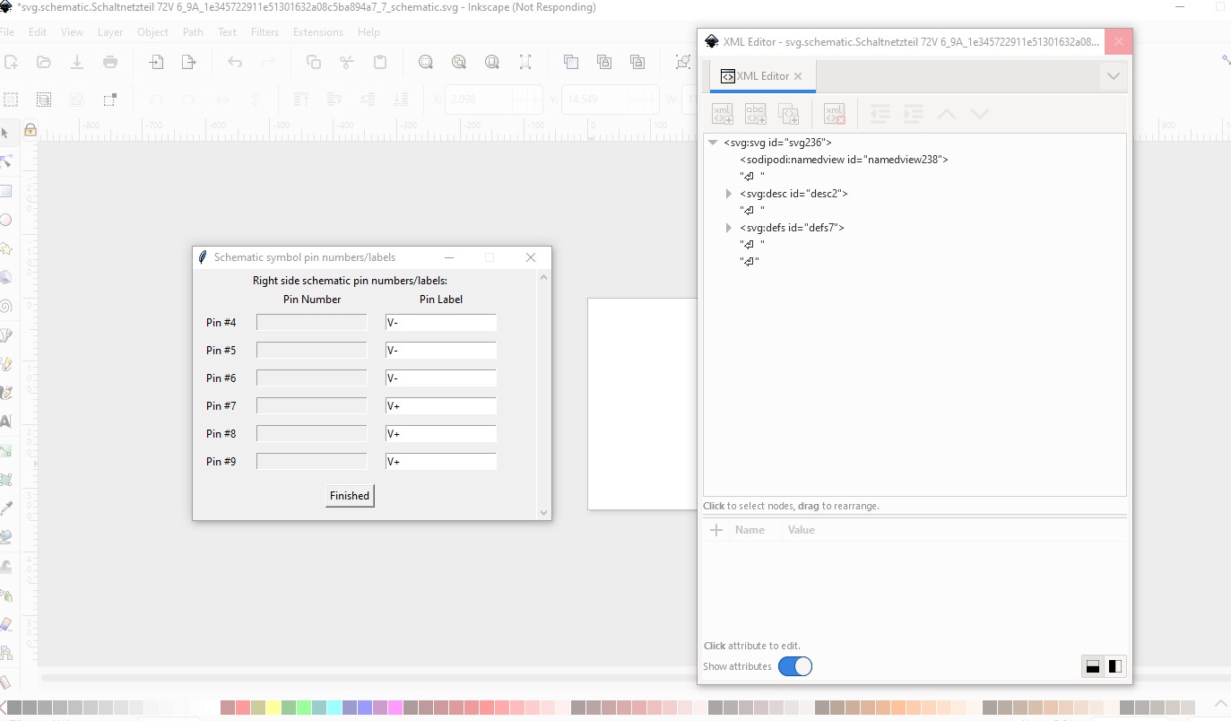
Then set the pin names for the connectors and hit finished to go to the right side and do the same there.
which produces this svg
which needs a little editing. Which results in the schematic svg which looks like this
we now have both the breadboard and schematic svgs and now move on to the fzp file. First set the current Fritzing version, and then change the version number from 4 to 1 (because this is the first version of this part!), add the fact I made changes to the part.
<module moduleId="Schaltnetzteil 72V 6_9A_1e345722911e51301632a08c5ba894a7_7" fritzingVersion="0.9.10" referenceFile="Antenna.fzp">
  <version>1</version>
  <author>Muecke82 (modified by vanepp Apr 2023)</author>
change the label from "Schaltnetzteil 72V/6.9A DC " to A (for assembly)
<label>Schaltnetzteil 72V/6.9A DC </label>
to
<label>A</label>
add some tags
  <tags>
    <tag>Power supply</tag>
    <tag>fritzing user</tag>
  </tags>
then reuse the breadboard svg as the icon svg from
    <iconView>
      <layers image="icon/Schaltnetzteil 72V 6_9A_1e345722911e51301632a08c5ba894a7_7_icon.svg">
        <layer layerId="icon"/>
      </layers>
    </iconView>
to
    <iconView>
      <layers image="breadboard/Schaltnetzteil 72V 6_9A_1e345722911e51301632a08c5ba894a7_7_breadboard.svg">
        <layer layerId="icon"/>
      </layers>
    </iconView>
then suppress pcb view by reusing the breadboard svg as pcb. from:
    <pcbView>
      <layers image="pcb/Schaltnetzteil 72V 6_9A_1e345722911e51301632a08c5ba894a7_7_pcb.svg">
        <layer layerId="copper0"/>
        <layer layerId="silkscreen"/>
        <layer layerId="copper1"/>
      </layers>
    </pcbView>
to:
    <pcbView>
      <layers image="breadboard/Schaltnetzteil 72V 6_9A_1e345722911e51301632a08c5ba894a7_7_breadboard.svg">
        <layer layerId="breadboard"/>
      </layers>
    </pcbView>
then delete the entire connectors section and replace it with a script generated replacement and set the pin descriptions to match the pin names in schematic.
  <connectors>
      <connector id="connector0" type="male" name="Pin 1">
        <description>L</description>
        <views>
          <breadboardView>
            <p svgId="connector0pin" layer="breadboard"/>
          </breadboardView>
          <schematicView>
            <p svgId="connector0pin" layer="schematic" terminalId="connector0terminal"/>
          </schematicView>
          <pcbView>
            <p svgId="connector0pin" layer="copper0"/>
            <p svgId="connector0pin" layer="copper1"/>
          </pcbView>
        </views>
      </connector>
      <connector id="connector1" type="male" name="Pin 2">
        <description>N</description>
        <views>
...
      <connector id="connector8" type="male" name="Pin 9">
        <description>V+</description>
        <views>
          <breadboardView>
            <p svgId="connector8pin" layer="breadboard"/>
          </breadboardView>
          <schematicView>
            <p svgId="connector8pin" layer="schematic" terminalId="connector8terminal"/>
          </schematicView>
          <pcbView>
            <p svgId="connector8pin" layer="copper0"/>
            <p svgId="connector8pin" layer="copper1"/>
          </pcbView>
        </views>
      </connector>
  </connectors>
</module>
Then add the bus definition to tie the 3 output pins to each other like this:
<buses>
 <bus id="V-">
  <nodeMember connectorId="connector3"/>
  <nodeMember connectorId="connector4"/>
  <nodeMember connectorId="connector5"/>
 </bus>
 <bus id="V+">
  <nodeMember connectorId="connector6"/>
  <nodeMember connectorId="connector7"/>
  <nodeMember connectorId="connector8"/>
 </bus>
</buses>
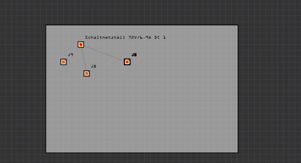
and the fzp file and the part are complete. So run the result through FritzingCheckPart.py to check for errors then test it. The end result looks like this in Fritzing. Breadboard is pretty much identical.
schematic is much smaller and the wires terminate properly
and pcb has only the pins that connect to the terminals the power supply doesn’t appear.
That is all contained in this part (it has the same moduleId as the current one so you will need to remove the current one before loading this one!)
Schaltnetzteil 72V 6.9A DC.fzpz (5.0 KB)
And finally here is the rather long output from FritzingCheckPart.py from the original part:
$ FritzingCheckPartw.py ‘part.Schaltnetzteil 72V 6_9A_1e345722911e51301632a08c5ba894a7_7.fzp’
**** Starting to process file Startup, no file yet
**** Starting to process file part.Schaltnetzteil 72V 6_9A_1e345722911e51301632a08c5ba894a7_7.fzp
**** Starting to process file svg.pcb.Schaltnetzteil 72V 6_9A_1e345722911e51301632a08c5ba894a7_7_pcb.svg.bak
**** Starting to process file svg.schematic.Schaltnetzteil 72V 6_9A_1e345722911e51301632a08c5ba894a7_7_schematic.svg.bak
**** Starting to process file svg.breadboard.Schaltnetzteil 72V 6_9A_1e345722911e51301632a08c5ba894a7_7_breadboard.svg.bak
File
‘part.Schaltnetzteil 72V 6_9A_1e345722911e51301632a08c5ba894a7_7.fzp.bak’
This is a through hole part as both copper0 and copper1 views are present.
If you wanted a smd part remove the copper0 definition from line 28
Modified 4: File
‘svg.pcb.Schaltnetzteil 72V 6_9A_1e345722911e51301632a08c5ba894a7_7_pcb.svg.bak’
At line 4
ReferenceFile
‘jumper_1_100mil_pcb.svg’
doesn’t match input file
‘Schaltnetzteil 72V 6_9A_1e345722911e51301632a08c5ba894a7_7_pcb.svg’
Corrected
Modified 3: File
‘svg.pcb.Schaltnetzteil 72V 6_9A_1e345722911e51301632a08c5ba894a7_7_pcb.svg.bak’
At line 8
Silkscreen, converted stoke from white to black
Modified 3: File
‘svg.pcb.Schaltnetzteil 72V 6_9A_1e345722911e51301632a08c5ba894a7_7_pcb.svg.bak’
At line 9
Silkscreen, converted stoke from white to black
Modified 3: File
‘svg.pcb.Schaltnetzteil 72V 6_9A_1e345722911e51301632a08c5ba894a7_7_pcb.svg.bak’
At line 10
Silkscreen, converted stoke from white to black
Modified 3: File
‘svg.pcb.Schaltnetzteil 72V 6_9A_1e345722911e51301632a08c5ba894a7_7_pcb.svg.bak’
At line 11
Silkscreen, converted stoke from white to black
Modified 3: File
‘svg.pcb.Schaltnetzteil 72V 6_9A_1e345722911e51301632a08c5ba894a7_7_pcb.svg.bak’
At line 12
Silkscreen, converted stoke from white to black
Modified 4: File
‘svg.schematic.Schaltnetzteil 72V 6_9A_1e345722911e51301632a08c5ba894a7_7_schematic.svg.bak’
At line 3
ReferenceFile
‘Schaltnetzteil-Schaltplan.svg’
doesn’t match input file
‘Schaltnetzteil 72V 6_9A_1e345722911e51301632a08c5ba894a7_7_schematic.svg’
Corrected
Modified 4: File
‘svg.breadboard.Schaltnetzteil 72V 6_9A_1e345722911e51301632a08c5ba894a7_7_breadboard.svg.bak’
At line 3
ReferenceFile
‘Schaltnetzteil-Steckplatine.svg’
doesn’t match input file
‘Schaltnetzteil 72V 6_9A_1e345722911e51301632a08c5ba894a7_7_breadboard.svg’
Corrected
Warning 6: File
‘part.Schaltnetzteil 72V 6_9A_1e345722911e51301632a08c5ba894a7_7.fzp.bak’
At line 2
ReferenceFile name
‘Antenna.fzp’
Doesn’t match fzp filename
‘Schaltnetzteil 72V 6_9A_1e345722911e51301632a08c5ba894a7_7.fzp’
Warning 11: File
‘part.Schaltnetzteil 72V 6_9A_1e345722911e51301632a08c5ba894a7_7.fzp.bak’
At line 45
Type female is not male (it usually should be)
Warning 14: File
‘part.Schaltnetzteil 72V 6_9A_1e345722911e51301632a08c5ba894a7_7.fzp.bak’
At line 67
terminalId missing in schematicView (likely an error)
Warning 14: File
‘part.Schaltnetzteil 72V 6_9A_1e345722911e51301632a08c5ba894a7_7.fzp.bak’
At line 82
terminalId missing in schematicView (likely an error)
Warning 14: File
‘part.Schaltnetzteil 72V 6_9A_1e345722911e51301632a08c5ba894a7_7.fzp.bak’
At line 97
terminalId missing in schematicView (likely an error)
Warning 14: File
‘part.Schaltnetzteil 72V 6_9A_1e345722911e51301632a08c5ba894a7_7.fzp.bak’
At line 112
terminalId missing in schematicView (likely an error)
Warning 14: File
‘part.Schaltnetzteil 72V 6_9A_1e345722911e51301632a08c5ba894a7_7.fzp.bak’
At line 127
terminalId missing in schematicView (likely an error)
Warning 14: File
‘part.Schaltnetzteil 72V 6_9A_1e345722911e51301632a08c5ba894a7_7.fzp.bak’
At line 142
terminalId missing in schematicView (likely an error)
Warning 14: File
‘part.Schaltnetzteil 72V 6_9A_1e345722911e51301632a08c5ba894a7_7.fzp.bak’
At line 157
terminalId missing in schematicView (likely an error)
Warning 14: File
‘part.Schaltnetzteil 72V 6_9A_1e345722911e51301632a08c5ba894a7_7.fzp.bak’
At line 172
terminalId missing in schematicView (likely an error)
Warning 35: File
‘part.Schaltnetzteil 72V 6_9A_1e345722911e51301632a08c5ba894a7_7.fzp.bak’
Connector1 doesn’t exist when it must to stay in sequence
Warning 19: File
‘svg.schematic.Schaltnetzteil 72V 6_9A_1e345722911e51301632a08c5ba894a7_7_schematic.svg.bak’
At line 1
Height 333 is defined in px
in or mm is a better option (px can cause scaling problems!)
Warning 19: File
‘svg.schematic.Schaltnetzteil 72V 6_9A_1e345722911e51301632a08c5ba894a7_7_schematic.svg.bak’
At line 1
Width 197 is defined in px
in or mm is a better option (px can cause scaling problems!)
Warning 19: File
‘svg.breadboard.Schaltnetzteil 72V 6_9A_1e345722911e51301632a08c5ba894a7_7_breadboard.svg.bak’
At line 1
Height 421 is defined in px
in or mm is a better option (px can cause scaling problems!)
Warning 19: File
‘svg.breadboard.Schaltnetzteil 72V 6_9A_1e345722911e51301632a08c5ba894a7_7_breadboard.svg.bak’
At line 1
Width 870 is defined in px
in or mm is a better option (px can cause scaling problems!)
Error 18: File
‘part.Schaltnetzteil 72V 6_9A_1e345722911e51301632a08c5ba894a7_7.fzp.bak’
Connector connector73pin is in the fzp file but not the svg file. (typo?)
svg svg.pcb.Schaltnetzteil 72V 6_9A_1e345722911e51301632a08c5ba894a7_7_pcb.svg.bak
Error 18: File
‘part.Schaltnetzteil 72V 6_9A_1e345722911e51301632a08c5ba894a7_7.fzp.bak’
Connector connector74pin is in the fzp file but not the svg file. (typo?)
svg svg.pcb.Schaltnetzteil 72V 6_9A_1e345722911e51301632a08c5ba894a7_7_pcb.svg.bak
Error 18: File
‘part.Schaltnetzteil 72V 6_9A_1e345722911e51301632a08c5ba894a7_7.fzp.bak’
Connector connector75pin is in the fzp file but not the svg file. (typo?)
svg svg.pcb.Schaltnetzteil 72V 6_9A_1e345722911e51301632a08c5ba894a7_7_pcb.svg.bak
Error 18: File
‘part.Schaltnetzteil 72V 6_9A_1e345722911e51301632a08c5ba894a7_7.fzp.bak’
Connector connector76pin is in the fzp file but not the svg file. (typo?)
svg svg.pcb.Schaltnetzteil 72V 6_9A_1e345722911e51301632a08c5ba894a7_7_pcb.svg.bak
Error 18: File
‘part.Schaltnetzteil 72V 6_9A_1e345722911e51301632a08c5ba894a7_7.fzp.bak’
Connector connector77pin is in the fzp file but not the svg file. (typo?)
svg svg.pcb.Schaltnetzteil 72V 6_9A_1e345722911e51301632a08c5ba894a7_7_pcb.svg.bak
Error 18: File
‘part.Schaltnetzteil 72V 6_9A_1e345722911e51301632a08c5ba894a7_7.fzp.bak’
Connector connector78pin is in the fzp file but not the svg file. (typo?)
svg svg.pcb.Schaltnetzteil 72V 6_9A_1e345722911e51301632a08c5ba894a7_7_pcb.svg.bak
Error 18: File
‘part.Schaltnetzteil 72V 6_9A_1e345722911e51301632a08c5ba894a7_7.fzp.bak’
Connector connector79pin is in the fzp file but not the svg file. (typo?)
svg svg.pcb.Schaltnetzteil 72V 6_9A_1e345722911e51301632a08c5ba894a7_7_pcb.svg.bak
Error 18: File
‘part.Schaltnetzteil 72V 6_9A_1e345722911e51301632a08c5ba894a7_7.fzp.bak’
Connector connector80pin is in the fzp file but not the svg file. (typo?)
svg svg.pcb.Schaltnetzteil 72V 6_9A_1e345722911e51301632a08c5ba894a7_7_pcb.svg.bak
Error 88: File
‘svg.schematic.Schaltnetzteil 72V 6_9A_1e345722911e51301632a08c5ba894a7_7_schematic.svg.bak’
At line 1
viewBox attribute missing
Error 69: File
‘svg.schematic.Schaltnetzteil 72V 6_9A_1e345722911e51301632a08c5ba894a7_7_schematic.svg.bak’
At line 18
Found a drawing element before a layerId (or no layerId)
Error 18: File
‘part.Schaltnetzteil 72V 6_9A_1e345722911e51301632a08c5ba894a7_7.fzp.bak’
Connector connector0terminal is in the fzp file but not the svg file. (typo?)
svg svg.schematic.Schaltnetzteil 72V 6_9A_1e345722911e51301632a08c5ba894a7_7_schematic.svg.bak
Error 88: File
‘svg.breadboard.Schaltnetzteil 72V 6_9A_1e345722911e51301632a08c5ba894a7_7_breadboard.svg.bak’
At line 1
viewBox attribute missing
Error 69: File
‘svg.breadboard.Schaltnetzteil 72V 6_9A_1e345722911e51301632a08c5ba894a7_7_breadboard.svg.bak’
At line 16
Found a drawing element before a layerId (or no layerId)
Error 18: File
‘part.Schaltnetzteil 72V 6_9A_1e345722911e51301632a08c5ba894a7_7.fzp.bak’
Connector connector0terminal is in the fzp file but not the svg file. (typo?)
svg svg.breadboard.Schaltnetzteil 72V 6_9A_1e345722911e51301632a08c5ba894a7_7_breadboard.svg.bak
Hope this helps!
Peter