Do you know of a tool that can convert *.sch (schematic) files to svg?
For example, there exists already a Schematic file for the Grove I2C Hub, which I would like to reuse for the schematic view in Fritzing.
Do you know of a tool that can convert *.sch (schematic) files to svg?
For example, there exists already a Schematic file for the Grove I2C Hub, which I would like to reuse for the schematic view in Fritzing.
I am using Autodesk Fusion and just found that this eagle2svg.ulp script works for me.
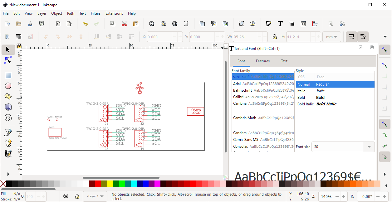
After creating the svg with the mentioned ulp script and loading the svg inside the schematics view of Fritzing, I get:
Also the imported schematic svg doesn’t look correct in Fritzing:
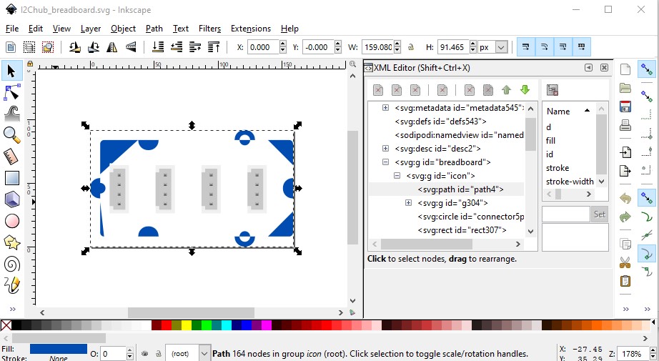
When I import the same svg into Inkscape it looks like this:
What can I do to fix the svg, so it can be used in Fritzing?
![]()
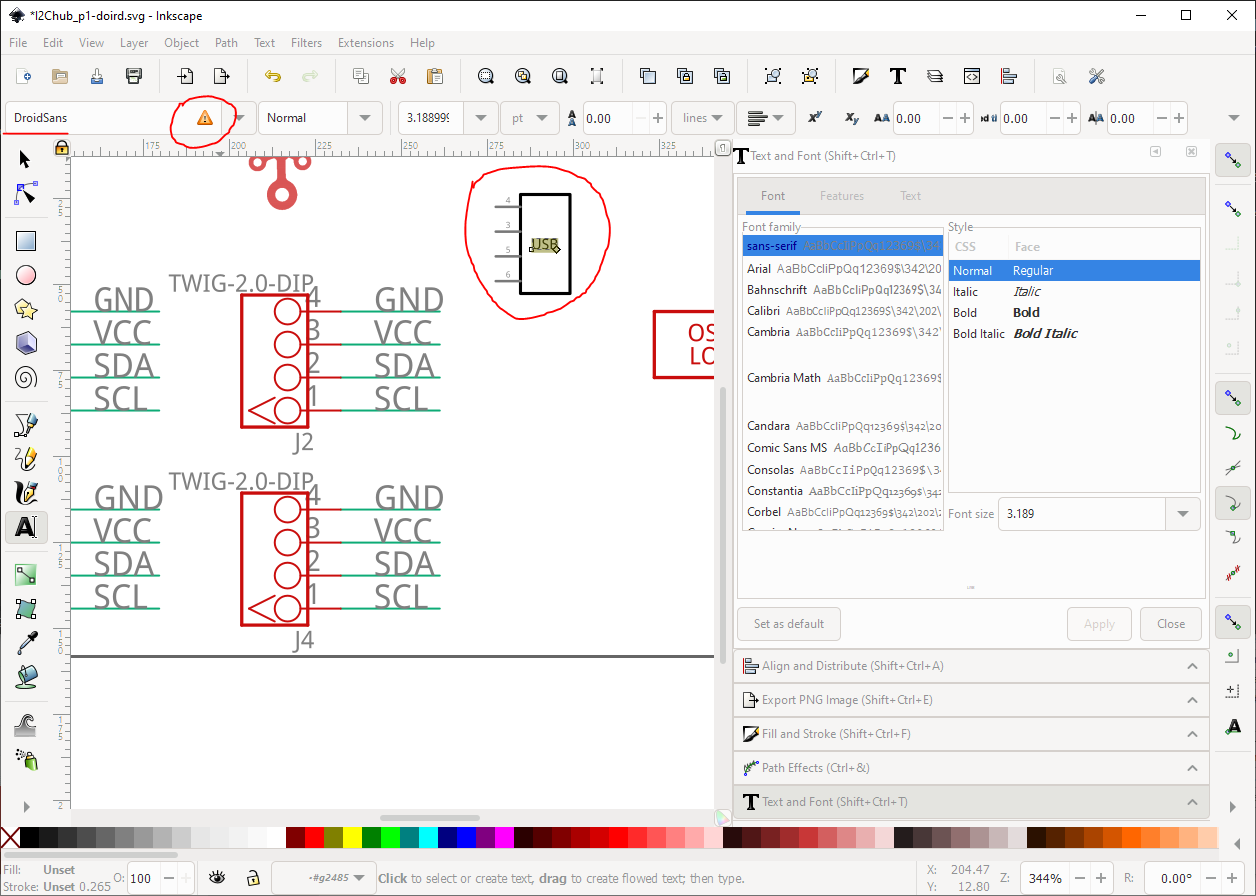
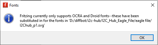
I just downloaded the Droid front from the fritzing tutorials and changed all the fonts in Inkscape to Droid Sans. I still get the same Fonts message mentioned above.
Here is the updated svg:
![]()
Any idea why this is still not valid in fritzing?
It seems that Droid Sans, which I have installed, is different to DroidSans? I just imported an “official USB schematic” and the font name is not found on my system:
Since there appears to be the eagle files on the Seeed site, there is a program called Eagle2Fritzing (which I have) which will create a Fritzing part from the Eagle files. I’ll run that and post the part in a bit. To build Eagle2Fritzing you need a Fritzing development environment which isn’t trivial to make.
edit: Here is a part. PCB is present (although probably not useful) but doesn’t have the board outline because Eagle2Fritzing screwed up the paths. I fixed breadboard but not pcb.
seeed-grove-i2c-hub.fzpz (10.4 KB)
Peter
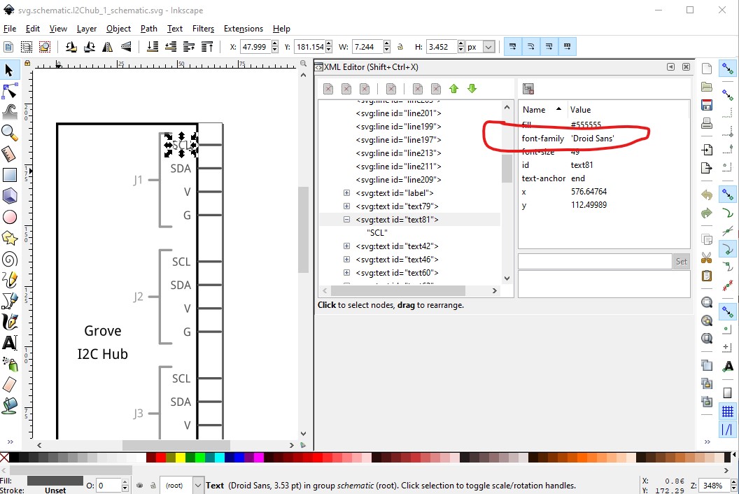
Spaces are important for font names, so yes, “DroidSans” is a different font than “Droid Sans”. The correct font for Fritzing is “Droid Sans”. It would seem that the ‘official’ schematic is incorrect. In some situations, an application can end up dropping the space from the name (or even dropping “sans”), unless the name has been put inside of quote characters: 'Droid Sans'. Other cases the quotes are not needed. What version of Inkscape are you using? When I openned the uploaded svg file on my Fedora 33 system, with Inkscape 1.0.2, I did not find any “DroidSans” references. Everything seems to (correctly) be “Droid Sans”. I also checked the the svg file directly (svg is xml, which is just text), and did not find any “DroidSans” in the file.
There are some additional requirements for creating an svg file to use in a Fritzing part. To start, for a schematic, the graphical content needs to be put into a group with an id (layer name) of “schematic”. The lines that are to be used as electrical connection points need to have id values as well, matching the connector for the part definition. There are also conventions and standards defined for the graphics. Much of which is not required to make a part work in Fritzing, but help to keep things consistent, so schematics views look reasonable, without some parts showing 10 times the size of others. See part file format and Fritzing’s graphic standards for some information. Peter has created an improved template file for schematic, but I do not have a link handy for it. I use a slightly different process that does not use a template to get the sizing right.
For the schematic view with missing content, there is not enough information here to tell what the problem (problems) could be. It will be something with the svg file itself, or with the part definition. They both need to be correct. The complete part file (.fzpz file) can be uploaded, instead of just a screenshot. That lets us look deeper.
As Peter indicated, starting from eagle files, using Eagle2Fritzing will probably give better results. When eagle files are available.
I am using Inkscape 1.0.2 on Windows but the uploaded svg file doesn’t contain any “DroidSans” reference as you noted. I wrote about the “DroidSans” font in the USB part that I imported to Inkscape. The USB part is directly from the Fritzing editor. I used this part and saved its schematic svg. I then imported this one into Inkscape and the Font of it was “DroidSans”.
Anyway, I was not able to load the svg I posted, which contains the “Droid Sans” font, in Fritzing part editor, without getting the Fonts Error/Warning message.
Thank you @microMerlin for the links I will try to get more acquainted with the Fritzing requiremtents.
Here is the complete .fzpz part file including the erratic schematic svg. I would be interested to know what the problem is and how to view all the lines and connections and get the font right:
Grove-I2C-hub.fzpz (21.1 KB)
Thank you for the part @vanepp . What would you suggest to fix the PCB view? I would probably try to convert the PCB from Autodesk EAGLE to svg (using some plugin if available) because I don’t have installed/compiled Eagle2Fritzing yet. In case you suggest to go with Eagle2Fritzing, is there a way to fix these problems. Would be great to know what the error/problem of Eagle2Fritzing was that you encountered. Having a working Eagle2Fritzing tool would be help a lot.
Thank you.
Actually there are three Droid Sans type fonts in the font file.
DroidSans.ttf font name “Droid Sans”
DroidSans-Bold.ttf font name - “Droid Sans” (don’t know how this is different that the one above though, although they look different on the screen in Windows!)
“Droid Sans Mono” font name - “Droid Sans Mono”
and I believe DroidSans works in Fritzing (although it is very possible it is being font substituted.)
There are also tutorials in the forum, these two apply to versions later than 0.9.3b (some of the others are for older versions.)
I suspect the font issue is with the font name (although I think this works for me, but I don’t use parts editor!) the font name here is DroidSans not “Droid Sans”:
compared to the schematic from my part:
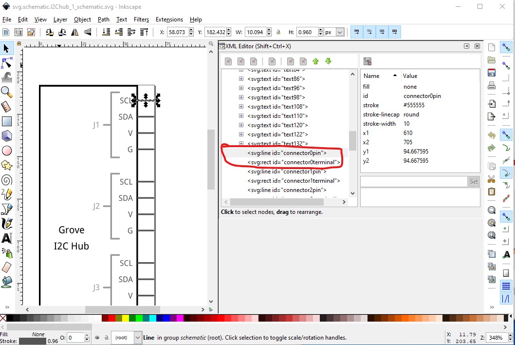
on the same text. As well your svg is missing connectorIds which will make it not actually work in Fritzing (and a layerId which is not as fatal.)
The entire drawing needs to be in a group and the group named the same as the layerId field in the .fzp file, in this case schematic like this:
As well the pins need labels that match the pin definition in the .fzp file like this:
without the proper connectorIds the svg won’t work in Fritzing.
The path for the board outline in pcb is (I think!) corrupted. The breadboard from eagle2fritzing looks like this in Inkscape:
It is possible this is because my version of eagle2frtizing was built 3 or 4 years ago and is based on Fritzing 0.9.3 (current version of Fritzing is 0.9.6 which has fixes for path problems in pcb and perhaps in general and may help.) I tried to edit the path, to correct it but I don’t know enough about manipulating paths to do it. So I added a blue rectangle underlying the path and added circles where the mounting holes should be to create the breadboard in the part. In pcb I would need to recreate the correct path and set the stroke width to 10 and fill to none to recreate the board outline. However since this is an existing board with grove connectors on it, it is unlikely anyone will use pcb so I elected to just delete the corrupted path and only leave the grove connector pins.
Peter
Loading your part into the editor, I do not get the message about the font. That was an information message (the “i” icon). The fonts were replaced, and the created fzpz file no longer has any problem with that.
I found out why some of the graphics is missing for the schematic. The svg file is defining a named style with css properties that specifies stroke and fill colors. The actual grphics elements have “class” attributes to pick those up. The current and previous versions of Fritzing support a superset of SVG 1.2 Tiny. That does not include defs and named styles. That covers most of what looks red in Inkscape. My assumption is that Fritzing is seeing that as stroke="none" fill="none", which is invisible.
To fix this, all of the class="«tag»" attributes need to be replaced by attributes to match the corresponding entry in the style2392 def. So a line element with class="l91" needs to have the class replaced by the line.l91 style information. Create a style="" attribute if it does not exist for the element, and add stroke:#0dab76; fill:none;. That is the most direct fix. I do not know how to get Inkscape to do that. svg files are plain text, and I am familiar with the structure, so for me, it would be easy enough to just use a text editor. A bit tedious, but not difficult. It would be simpler (for me) to just create a new schematic svg from scratch. I do not much like the way the imported image looks for schematic view, and this looks like a good place to use the optional subparts feature of schematics. That would allow the individual I2C connectors to be moved around the schematic independently. This part also needs to have bus definitions to show that the 4 connectors are tied together.
The schematic svg does not have any connector or terminal elements defined, but that can be done from the Parts Editor, once the other graphics problems are resolved. The correct (currently invisible) elements need to be associated with the proper connector definitions.
The text is a bit different size, because another Fritzing limitation, is that it does not like units on font size attribute values. The svg file has things like style="font-size:2.60773px" To get Fritzing to get the size right, that should be style="font-size:2.60773"
Peter created a python FritzingCheckPart tool to help detect and cleanup some types of problems with part definitions and svg files. That reports issues with the other view svg files as well. The important problems are:
The part definition is set for through hole connectors (both top and bottom, copper1 and copper0 layers), but the pcb svg only has copper1. Either need the second copper layer on the pcb svg, or remove it from the definition. I think parts editor has an option to switch between smd and thd. Like Peter, I do not normally use the parts editor. There is a learning curve, but parts can be created and edited without it. The parts editor is not ‘complete’, and there are lot of things that can be done manually, that the editor can not handle.
The breadboard svg is missing the layer wrapper, just like I mentioned earlier for the schematic. It also has the drawing dimensions in px (pixel) units, which is not consistently reliable. For a CADD style drawing, real world units (in for inches, mm for millimeters) are much better. Fritzing tries to convert, but it is not always correct.
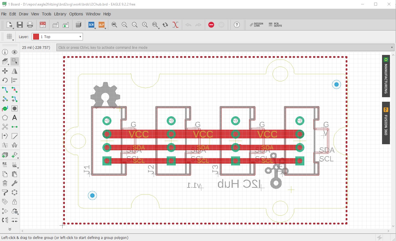
The PCB svg does not have enough connectors for what is specified in the definition. I do not know what should be on pcb view. Is this a stand alone breakout board? How would this connect to a pcb in a project? The pcb view of the part you uploaded implies a 5 bin smd connection, but that does not seem right. Given the parallel connection nature of the hub, it is quite possible that there are few external connections, but the part definition (and maybe svg) need to be adjusted to account for that.
I recognize the symptoms. It looks like either some sub shapes are not being closed (missing “z”), or fill is set to a color when it should be “none”. With the circles, it could also be that the interior cutout is going the wrong direction (CW version CCW) compared to the outer shape. I do manipulate path elements.
I2Chub_breadboard.fzp (97.7 KB)
Here is a zipped copy of the svg (as usual, the forum says it can’t determine the size of the raw svg) if you would like to have a bash at the path. It is a long one and I don’t know enough about paths.
Peter
When you fixed the bb svg, did you just add a rectangle and some circle elements, or did you also delete a path element? The somewhat strange path element I found looks (partly) like it is intended to be a shadow at the edge of a bb with rounded corners. To create a 3D effect. Ignoring the possible 3D shadow, I would replaced the rect, path, and white circles with a single, considerably simpler path containing the circle cutouts. 4 arcs for the corners, 6 semi-circles for the edge cutouts and extended mounting holes, horizontal and vertical segments to connect them, and 3 circular cutouts for the mounting holes.
The posted svg is what eagle2fritzing produced with no changes. I added some circles and a rectangle over top of the path (I don’t think I deleted anything) to create the correct board outline.
edit:
The path also looks fine in eagle, so it looks like it was eagle2fritzing that had the problem. I don’t know if the path fixes in 0.9.6 would help with this or not they may be only for gerber generation.
Peter
Here is zip of the cleaned up breadboard view, plus a copy scaled to 10 times size (I changed the main height and width to 9.5 by 16.5in) so the forum would let me post it directly as well. This includes cutouts on the board for the header pins. I also re-scaled it so 1px = 1mil. The spacing seem a bit odd. The header pins are 78.74mils apart vertically, the headers are 375mils apart horizontally. Does that match the datasheet (or eagle)?
I2Chub_breadboard.fzz (2.0 KB)

Thanks, I’ll poke at this and see if I can figure out what you did  (and steal and use your path in breadboard and pcb of the part!) The scaling seems a little off, the connectors are 2mm pitch and in my breadboard svg are in fact at 2mm pitch, but in your svg they seem to be a little high 20.762mm. I’ll poke at that as well, I may have corrected the pins on breadboard to be 2mm, I certainly reduced the size of the pins and changed the offsets a bit as I’m too lazy to bump the offsets in eagle2fritzing, I find it easier to just edit the resulting svg in Inkscape.
Peter
With some real numbers, from datasheet or eagle, I can tweak the positions fairly easily. The internal structure is a repeating pattern that is setup to be able to do (simple) bulk edits.
78.74mil spacing is about right then. That calculates to 1.999996 mm. Or going the other way, 2mm is 78.74016 mils (rounded). I do not know where you get the 20.762mm (probably a typo from 2.0762?) since that is over instead of under.
So that is why the holes in the board do not quite match the position of the header pin graphics. I was wondering.
If the rest of the board measurements are in mm, I should have converted from inches to mm. The numbers would have been better. Unit and scaling conversions are “easy” once you know the math and understand the relation ship between drawing units, viewbox, svg scaling, and px units.
As far as what I “did” for the path, don’t try to compare with the original. It is seriously messed. I just used it to pull coordinate and radius values from, overlaid my own version to get a good match with clean numbers, and deleted the original.
I can create a silkscreen outline from that path, without the connector pin holes if you want. Just would like confirmation that the board dimensions are close to correct. Directly “stealing” the path will only work if the other drawing is set to 1px = 1mil. Adding a transform=“(scale())” to the path would handle the difference.
From Inkscape by subtracting connector6pin y position ( 104.917mm) from connector5pin y position (84.155mm) which gives 20.762 which dividing by 10 for the scale gives 2.0762mm pitch. I’ll poke at the eagle file and see if I can find dimensions. The web site says 40mm by 20mm but it is unclear what is included in that measurement. Eagle seems to indicate that it should be 42.5mm by 23.5mm to the edges of the board (approximately, it is snapping to a grid that doesn’t exactly match the board outline.)
edit:
Used the new path in breadboard and pcb. In pcb the path renders in Fritzing correctly but doesn’t appear in the gerber output (only the connectors) although I don’t see any issues in the pcb svg (i.e. no translates.) Appears gerber processing doesn’t like something about the path, I don’t know what.
seeed-grove-i2c-hub.fzpz (10.5 KB)
Peter
Connector5pin was out of position (in y) by 3mil. Something missed during some of the bulk edits. With that fix, the connector5pin to connector6pin delta y is 78.74 mil = 1.999996mm, which is what it should be.
My drawing came out to 1.6574in by .95307in, which is 42.098mm by 24.208mm. The ‘bumps’ for the mounting holes were 82.5mil, or 2.1mm. That comes out very close
42.098mm by 24.208mm versus
42.100mm by 24.200mm
Bad svg and zip replaced in the previous post.