is there a complete list of layer names to use when designing components in a vector package (using inkscape here).
have tried google and there doesn’t seem to be an actually complete guide to doing this.
managed to create a component that works in breadboard and schematic view, got something that physically puts pads where I want them for PCB, but only then allows connections to the centre of the component - and can’t find how to define drill holes and locations, or stuff like slots, plated and un-plated.
also is there a standard set of colours for stuff like silk screen items. I’ve tried looking at the template items but seem to have a few issues, e.g. copy & paste causes all sorts of problems (copy a pad and the original pad is fine the copy looks like an 8 bit image from the 80’s.
worked around that one but I’ll be dipped in sugar if I can work out how to specify a dill hole.
trying to make elliptical pads due to component pin spacing, I guess this is a case of define the ellipse then “somehow” drill a hole though it? presumably by drawing a circle somewhere?
Documentation is unfortunately lacking. Someone capable of and willing to write documentation is highly desired, we just haven’t found someone yet . Here are two tutorials that apply to the current version of Fritzing (most others are for older versions of Fritzing):
If you find parts that are unclear in mine, feel free to post and I will try and fix them up, Old_Grey hasn’t posted in a while and I think may have moved to Kicad as the project he is involved in what moving that way. Now for direct answers to your questions (I also use Inkscape):
pcb wants by default (it is actually specified in the fzp file for the part in the layers section) these groups in this order:
Through hole part:
group silkscreen
silkscreen drawing elements
group copper1
group copper0 (this is a subgroup of copper1
copper drawing elements (usually a circle for a connector pin, but sometimes something like a path for an oblong connector). There are other fields available but these 3 are the common ones. A SMD part omits the copper0 layer so has only silkscreen and copper1.
As far as I know this is the only way connections will be made in pcb.
In Inkscape a hole is created by a circle with a stroke-width of 20thou (which depends on drawing scale). The hole size = circle-diameter - (2 * stroke-width), so for a .1 header (where the hole wants to be 0.038in, the diameter of the circle wants to be 0.078in with a 20thou stroke width that creates a 0.038 hole in the gerber output. You can also do this with a circular path (but only a circular path, oblong doesn’t work as far as I can tell), but a circle is preferred because it is easier to change later. Oblong pads as you want are created by overlaying a oblong path over a circle (whose id is connectorxpin where the path is unnamed both in copper0 as SMD doesn’t drill holes.) I can point you at parts with oblong pads if you like, often copying an existing part is the easiest way to make parts.
Yes, they are defined in the graphics standards here:
the part file format is also a very useful document:
All of that said, the usual way (and the way I learned to make parts) is to ask questions here, preferably uploading the .fzpz file of the part you are making so one of us can look it over and tell you what is wrong. Upload is 7th icon from the left on the reply menu.
cheers, useful stuff. have had a fiddle and think I now, more or less, have a workable component.
further question, how do you include a slot? component I have includes a blade like assembly as a combined grounding point and mounting fixing. needs a plated slot to sit in?
Sorry, forgot that one. It is difficult, Fritzing (and most board houses apparently) don’t do well with slots. There are a series of forum posts on the subject, but I can never make the add/subtract paths work correctly. @opera_night 's posts in the tutorials and guides section of the forum are the best bet. Search for slot in the forum search bar or for posts by @opera_night should turn them up. Be prepared to experiment and get frustrated, because there are also bugs in the process I think. As noted I have never been able to make it work.
Graphically, is a slot a shape with a hole cut out of the middle? If so, the trick for the add/subtract paths (using a single path object) is to create and close the outer shape, move to a position on the edge of the inner cutout, then create that shape going in the opposite direction from the outer shape.
That is what I am doing for the oblong pads for the LED matrix parts, and it is what was done for (at least) the MAX7219 and 556 pads. I discovered that method by accident when I was first learning to build svg files by hand.
Convincing Inkscape or Adobe to do that could be a challenge. I have always done it by directly editing the “d” attribute of the path.
An explaination on how to do this would be appreciated, as lots of folks want to do it. @opera_night seems to be able to make it work in the various svg editors, but I have had no success, but I don’t know much about paths either.
I’ve been looking at and collecting the tools to create a screencast for creating the cutout shape in Inkscape. Before start staying “this will work” though, is there a part around, maybe created by @opera_night, that includes a slot, and works? I can easily create what looks like the needed shape/svg element, but can not confirm that the result produces the proper gerber file. I need a working sample. What I have worked on so far only expands circular pads to oblong, and even then, I do not know if the gerber is really correct. That is not something I have needed yet.
@opera_night uses a cnc mill to make boards, so for him the slots work. As I understand it (but could be wrong) the cheap board houses don’t do slots and I think that Fritzing does not create the correct gerber output to make slots for board houses that can. Perhaps one of the Aisler folks will comment as they know way more about board production than I do. The way people have made slots for USB connectors is to drill an overlapping series of holes in the slot then file off the rough edges. They say the board houses usually don’t have a problem with overlapping holes (I would think it would tend to break drills!) but I have not tried it.
I think both would be valuable, there are a few people doing boards with cnc routers which can do the slots, it is only the board houses that are more difficult (and maybe not possible.)
I’m in Vancouver so we are almost neighbours , I have no idea what a Zoom session is though, I’m old and reasonably luddite about the new technology, I grew up on command line and GUIs are a stretch I still do a lot of work on the command line.
Zoom home page
Video conferencing, screen sharing, remote control. I could for example use it to directly demo the steps needed in Inkscape, and have interactive feedback to answer questions, or expand on the demonstration.
You might be older than I am, but not by that much. I have been doing computer programming for 40+ years, and learned electronics before that.
Vancouver eh? I am President of a local robotics group. One of our active members moved to Osoyoos, and has been joining us remotely. So he is even closer.
Zoom may be something to try later, right now my network connection is hosed. A couple of weeks ago Telus came by and pulled fibre in to my basement. Unfortunately pulling the fibre (by pulling out an unused Shaw cable coax) looks to have jarred my 42+ year old cat 3 connection and ADSL is almost dead. At small volumes like email and this all is well ~30msec ping time to the Telus gateway. However a load (such as a file transfer) ping latency increases that to more than a second (and it sometimes cuts out entirely.) I suspect because of retransmissions to the DSLAM. Since I will upgrade to the fibre option when they can, it is so far not worth trying to fix the adsl since I expect they would have to repull the cat3 to correct it. I note Zoom says sign up is free, but is using it free (seems unlikely …?)
Using it is still free. Limit of 40 minutes per session if more than 2 connections in the meetings. I used it to run a screen share/remote control session for 7 hours straight yesterday. Previously for a couple of hours for one to one video conference, and testing out various options. If going more than two people, then the limit is 40 minutes. Some options not available for the free plan, but it is still very usable. For the added features, only the host would need a paid plan. Guests can still use free.
EDIT: Free zoom also runs on smartphones, but that would get expensive in air time, unless connected to wifi. I don’t suppose you have (can get) wifi that is at the other end of the jarred cat 3 cable?
Before start staying “this will work” though, is there a part around, maybe created by @opera_night, that includes a slot, and works? I can easily create what looks like the needed shape/svg element, but can not confirm that the result produces the proper gerber file. I need a working sample.
Truly, I’m not performing any magic, I’m simply using most any Graphics program and/or simple Text Editor to do it. I’ve posted how-to-do-it too many times so, won’t repost.
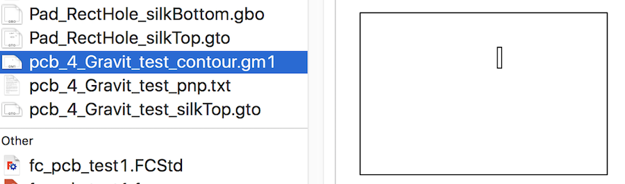
However, as an aid, Attached are some files that could help. NOTE: for some reason, attachment files with tricked extensions no longer work/upload, nor does uploading the SVG’s text.
So, the attachments that may help are screenshots:
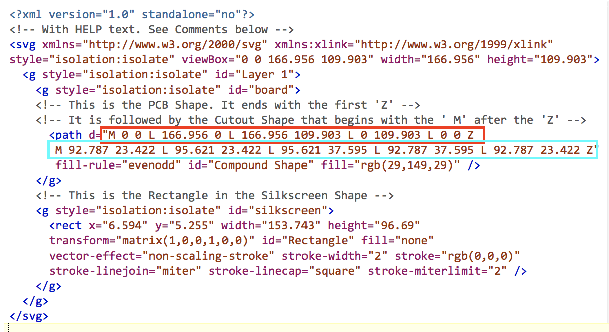
The SVG image and it’s text (simply create a text file with the info and it should work. Then, you can tweak the Path’s data to change the shape. And, more importantly, understand all the elements of the text (layers/etc…, so you can move forward to other/more complex cutouts). Be sure to locate my posting on SVG’s intrinsic subtraction. Hint: the board shape should go Clockwise, and the cutouts go CounterClockwise. But, not always… depends… When you create the board and cutouts by drawing lines, draw them Clockwise and CounterClockwise… get it!
Note: You can make the board/file so Fritzing will recognize a ‘cutout’ as a cutout but, that’s only an internal name recognition, it has nothing to do with the actual cutout so, I don’t fuss with it. Just ignore any messages about board not having cutouts. I’ve posted info on this subject…
Regarding making the boards. Many board fab houses use CNC or Laser for cutting so, rectangles/other are not a problem (CNC will leave radius’d corners and Laser’d corners will look rectangular.
This is an unfortunate feature of the upgraded forum software, it now finds svgs renamed to .fzp and tries to render them. For svgs, after the upload look at the upload text in this window. Typically the size of the svg is too small (3*4 pixels for instance) and multiplying that by 10 or 100 makes the svg render most of the time. Of course right now when I tried to upload one to demonstrate it is telling me “sorry we couldn’t determine the size of your svg, maybe it is corrupted” with perfectly good svgs.
Perhaps this will help - I added some comments to the SVG’s text to clarify…
It should serve as a Basis (for anyone wanting to make a PCB with Cutouts).
Red rectangle is the PCB shape.
Turquoise is the Cutout shape.
EDIT: Typing the above text, Be Sure To Use UTF-8 Plain Text font!!!