I created a new part smd package for a chip that was already available as DIP package. I noticed that some pins seems to be “interconnected”. That means, that if for example try to lay a new wire in the schematic new and click on one pin (23) I can see pins 15, 35 & 43 being highlighted as well, which doesn’t make sense. I also get this behavior from pin 24 highlighting pin 44.
I checked the numbers on the pins for the symbol and pcb image. I checked the connections in the Part’s editor, but everything seem to be OK. Any ideas what I might need to check?
You look to have not changed the bus definitions from the atmega32u4-qfn2 part you cloned from (the dip 40x2 part would probably be a better starting point though.) In the fzp file this section is not correct:
presumably it is correct for the atmega32u4. I would start from the 40x2 dip part and replace the pcb svg with the one you used in this part (checking the pin numbers when you are done.) The following tutorials on parts making may help as well.
Yes, I did get the breadboard schematic from the atmega32u4 as well as the pcb footprint. The symbol and the icon images came from the dip version of the chip. I don’t recall seeing any “buses” options in the image’s SVG files or the part’s editor.
I will start again re-creating the part. Thank you for creating those videos!
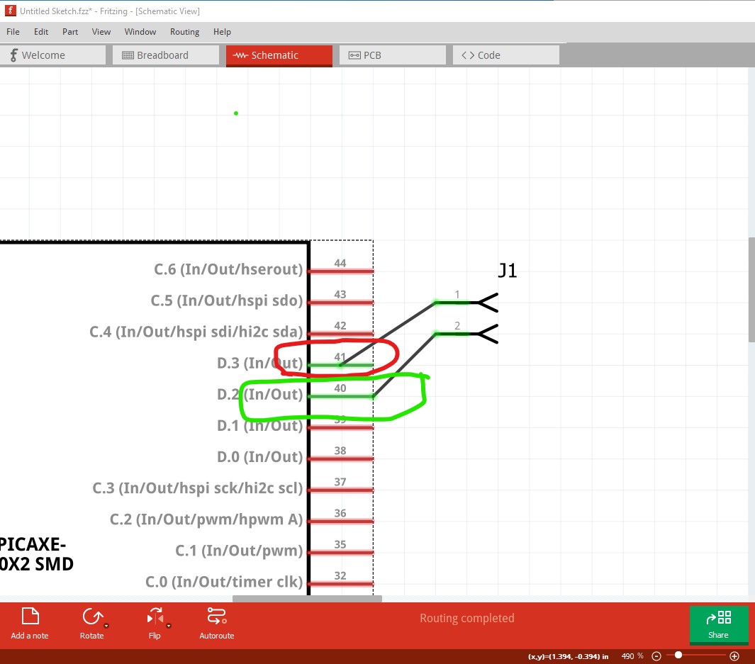
In parts editor they are called internal connections. I don’t know that you can delete them in the parts editor (I rarely use it) but you may be able to. You can set them in the parts editor although that may leave the existing ones. Starting from the 40x2 part and replacing the pcb svg with the one from your part is going to be the best bet as the pin names in the .fzp file also appear to be wrong and 4 pins are missing (pins 12, 13, 33 and 34 in breadboard are not connected to anything.)
I didn’t see any options in the Part’s editor, so I corrected them by hand, when I made the part again. Those 4 pins are NCs (not connected), so I left them out.
Another issue that I noticed is that when I rotate the part in the PCB view the nets are not following along unless I also move the part a bit, up, down, etc. Could it be due to the pcb image file?
Got it! It seems a copper0 tag left under the copper0 tag, in the pcb svg file, created this issue. I removed the tag and the issue is now resolved!
For anyone needing this part, I have attached it here:
The .fzp file needs some fixes. It is currently a through hole part (with both copper1 and copper0) but as an SMD part it should only have copper1 (no copper0). In the fzp file
As well the .fzp file has terminalIds defined but they aren’t in the breadboard svg. Fritzing will ignore them so they don’t need to be fixed particularly.
I figured out the copper0 issue when I needed to export the gerber files. It’s already corrected and works fine. As for the terminals, I completely missed that. I can see the issue in the schematic. I have now corrected the part and posting it again.