No Drill Holes on PCB for Custom Parts

I am trying my hand at making my own custom parts and I am running into an issue where there are no drill holes detected when I check my board.

I am trying something basic to troubleshoot this issue.

I am using InkScape with layers copper0>copper1 and silkscreen.
I have changed the IDs for each layer in the XML editor to match the layer names.
I have just two circles at this time, no silkscreen. They are 2mm with no fill and a stroke width of .3mm.
The stroke color is R247, G189, B19.
I have edited the XML for the two circles to be connector0pad and connector1pad.
I Save A Copy as a Plain SVG in InkScape.
When I load the PCB image in the Fritzing Part Editor, it looks ok. Not quite like the core parts, but I am able to connect traces to the core part (R1) and the routing rules check out. When I check the board, my parts have no drill holes.

Any ideas what I am doing wrong? Thanks
custom_part_a

custom_part_b
custom_part_c

Most likely your pads are ellipses not circles (uploading the .fzpz file of your part rather than images is the best bet, upload is 7th icon from the left in the reply menu!) if the pad is an ellipse no hole is generated. FritzingCheckpart.py warn you when that is the case as well. This tutorial on parts making may help as well.

Peter

Thanks! You were right. I converted the ellipses to paths (Path>Object to Path) and that fixed my problem. Now I will go through your tutorials and do this correctly. The info out there including YouTube leaves a lot out. Thanks so much!!!

Actually converting to paths is undesirable. It makes changing the hole size more difficult. The preferred method is to restore the ellipse to a circle by setting the two radii (rx and ry) to the same value then moving the circle in x or y one position left or right then back via the tool bar. That causes Inkscape to convert it to a circle (with a single radius r.) This is desirable because in Inkscape the hole size is set by hole-size = pad-diameter - (2 * stroke-width) which is much easier to change than a path.

Peter

Yep, seeing that in your tutorials. Thanks.

Thank you again for the tips. The custom part stuff is working great for the PCB. Do you have something on creating custom breadboard parts? I want to create custom parts for the way I layout components, but I can not get the pin spacing correct. I can’t seem to fin the specs on doing that. Most of the parts I see tutorials for are more IC and Boards. I just need to create some simple parts. Thanks again.

Is about as close as there is. Pin spacing is easy, just use the tool bar with the dimensions set to in and space the pins. Here I set the tool bar to in and pin 0 is at x 0.021in and y is 0.02in

pin1 is at x 0.072in y 0.021in. To set the pin spacing start from the pin0 x coord and add the spacing in inches that you want (in breadboard that should typically be 0.1in to stay on the grid, but can be the actual spacing between pins.)

Same for y although that isn’t shown here. Note the start point in the lastest version of Inkscape is the top left of the drawing element. In earlier versions it was bottom left.

Peter

I will give this a try, thanks!

I am just not getting this. This is with just a simple shape to try and figure out the size and spacing. Here is a core part compared to mine. I am off center of the grid and I cannot figure out how far the connectors should be spaced so they both connect. Any help would be appreciated, although, I understand if you are done answering my stupid question. Thanks.
ftz_bb

Upload the breadboard svg file (upload is 7th icon from the left) and I’ll have a look. Two possibilities are you don’t have any connectors defined (Fritzing will snap a random connector to the grid which can cause offsets if the pins aren’t on 0.1in spacing) or you haven’t done Edit->select all then Edit->resize page to selection which leaves the starting x/y coords non zero which will cause an offset like this. The last one appears somewhat more likely because it looks like the left side connector has connected as the breadboard pins are green but right side has not (which may be that it is slightly too far off to connect.) The real reason should be easy to tell from the svg.

Always happy to help people make parts. We don’t have any where near enough people making new parts these days compared to 5 years ago (when there were 4 or 5 people capable of making complex parts!)

Peter

test custom parts.fzz (7.4 KB)
Here you go thanks. I am sure I am doing something stupid that I will slap my forehead for.

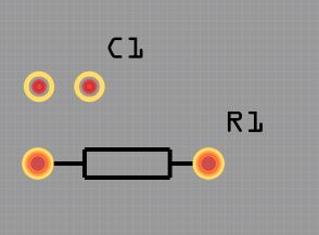
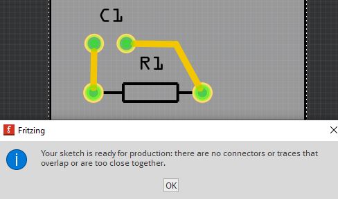
OK, good thing you didn’t upload just the svg, because the problem isn’t there (there are problems, but not the misalignment!) So lets start with the breadboard svg and fix it up (although it technically will work as is because it is correct!)

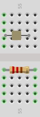
It is correctly set to start at 0 0

The pins are in the correct place and at the correct spacing (on 0.1in boundaries)

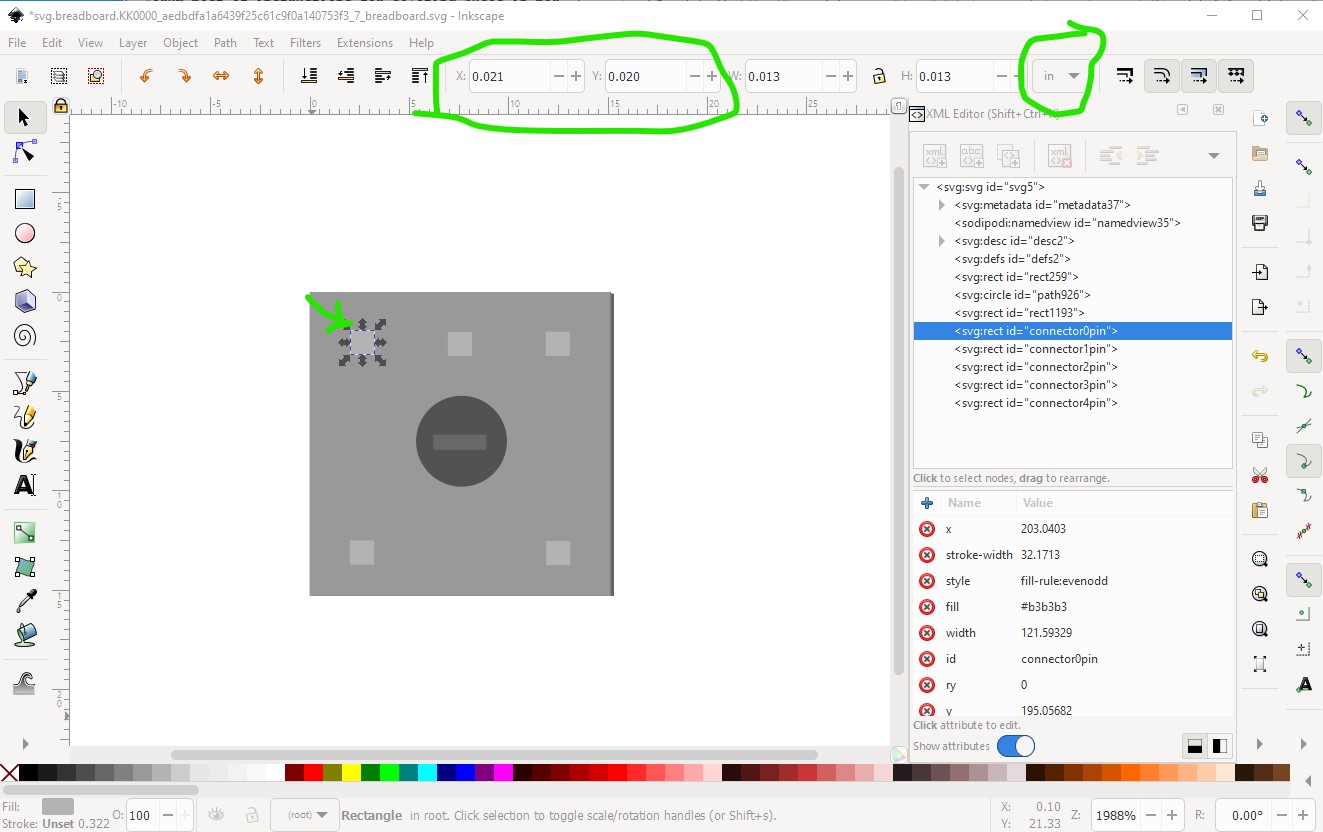
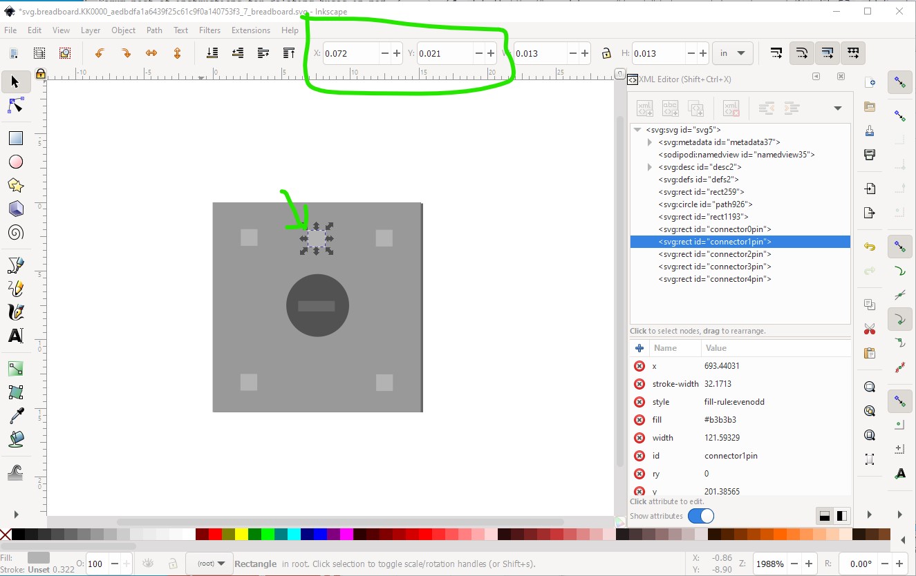
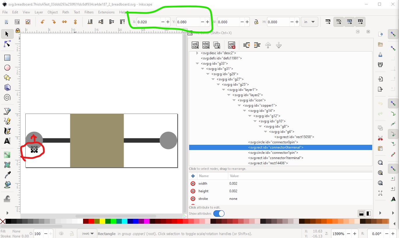
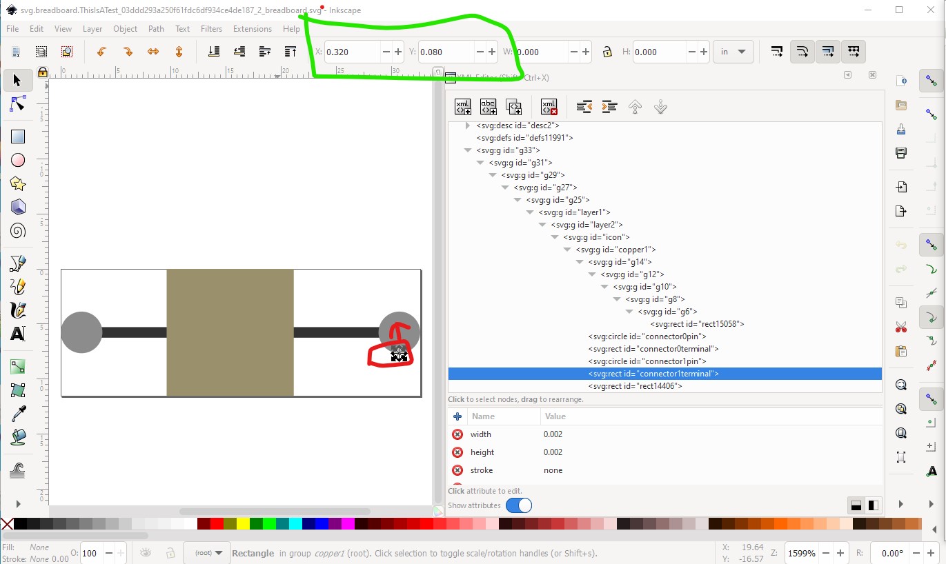
the terminalIds are as well, but they are offset a bit (and technically are not needed the pins alone will do in breadboard!) They need to be in the center of the circle not at the bottom of it.

You have an icon and copper1 layerId but not the required breadboard layerId here

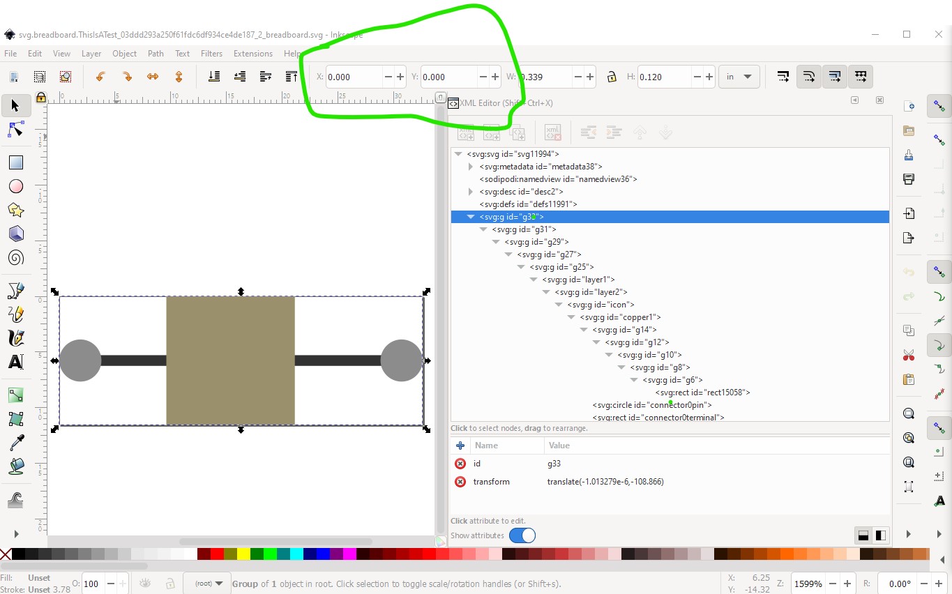
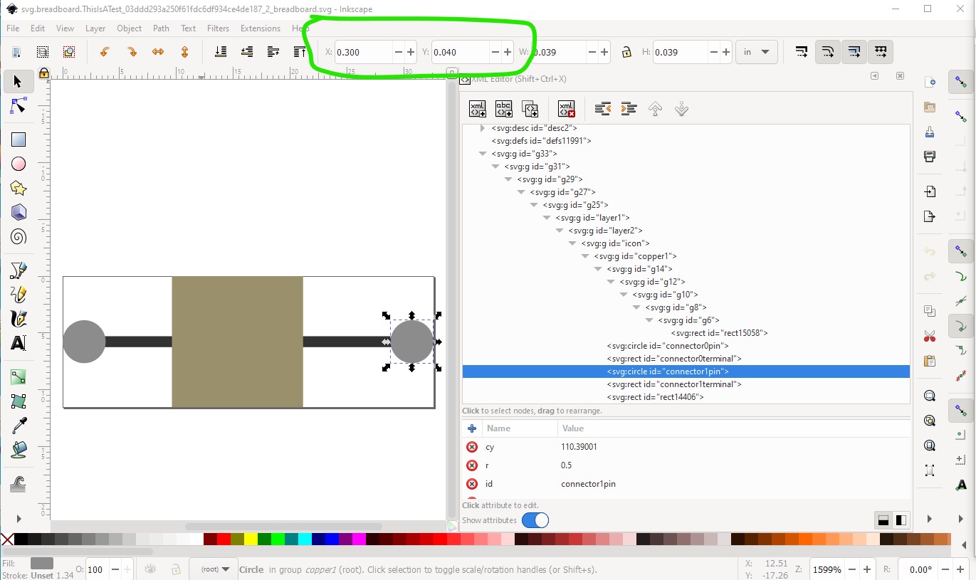
So to fix this I ungrouped the entire svg like this (selected the top group and then hit cntrl-shift-g multiple times to ungoup.)

and removed the terminalIds as unneeded. Then I regrouped the entire svg and set the group id to breadboard to create a correct breadboard svg.

Then I changed to the .fzp file which is where the problem is. You look to have cloned this from a resistor, which is a bendable leg part. Parts editor should have given you a warning that it does not support bendable leg parts which is why there is a problem here.

<connectors>
  <connector name="Pin 0" id="connector0" type="male">
   <description>Pin0</description>
   <views>
    <breadboardView>
     <p layer="breadboard" legId="connector0leg" svgId="connector0pin"/>
    </breadboardView>
    <schematicView>
	...

This is connector0’s definition in the .fzp file. The line

     <p layer="breadboard" legId="connector0leg" svgId="connector0pin"/>

is for a bendable leg part. For your setup it needs to look like this:

     <p layer="breadboard" terminalId="connector0terminal" svgId="connector0pin"/>

for my modified breadboard svg it needs to look like this

     <p layer="breadboard"  svgId="connector0pin"/>

I expect the legId being missing from the svg file is what is causing the pin offset in breadboard. This fixed .fzpz now works correctly.

This is test-fixed.fzpz (6.8 KB)

so the problem was a Fritzing oddity. FritzingCheckPart.py will also flag this error like this (although perhaps in a not very clear way since, it assumes you know what the xml should look like!):

$ FritzingCheckPartw.py part.ThisIsATest_aa11546556d623bd23ac862976def415_2.fzp


Error 69: File
‘svg.breadboard.ThisIsATest_03ddd293a250f61fdc6df934ce4de187_2_breadboard.svg.bak’
At line 22

Found a drawing element before a layerId (or no layerId)

Error 18: File
‘part.ThisIsATest_aa11546556d623bd23ac862976def415_2.fzp.bak’

Connector connector0leg is in the fzp file but not the svg file. (typo?)

svg svg.breadboard.ThisIsATest_03ddd293a250f61fdc6df934ce4de187_2_breadboard.svg.bak

Error 18: File
‘part.ThisIsATest_aa11546556d623bd23ac862976def415_2.fzp.bak’

Connector connector1leg is in the fzp file but not the svg file. (typo?)

svg svg.breadboard.ThisIsATest_03ddd293a250f61fdc6df934ce4de187_2_breadboard.svg.bak

Here (among other things!) it has noted the lack of a breadboard layerId and that there are not legIds in the svg file. It is depending on you knowing what a legId is for and what to do about it though. Here I changed just the fzp file to set the legIds to terminalId and terminal which clears the error:

Warning 20: File
‘svg.pcb.ThisIsATest_03ddd293a250f61fdc6df934ce4de187_2_pcb.svg.bak’
At line 72

copper1 layer should be at the top, not under group copper0

Error 69: File
‘svg.breadboard.ThisIsATest_03ddd293a250f61fdc6df934ce4de187_2_breadboard.svg.bak’
At line 57

Found a drawing element before a layerId (or no layerId)

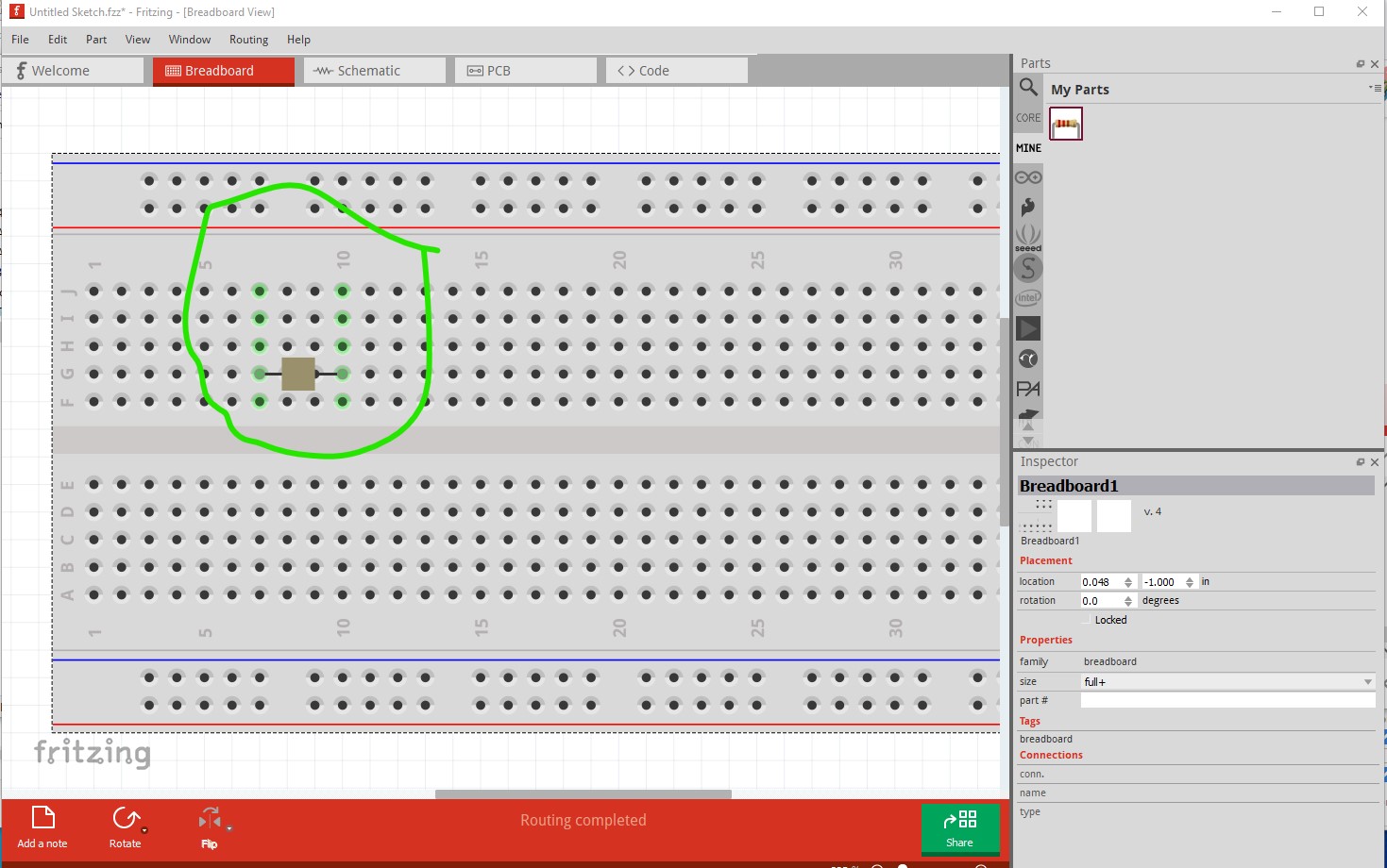
which now works although it is slightly offset due to the terminalIds being misaligned (Fritzing is aligning to the center of the terminalId in this case, it has connected correctly but the pins are slightly offset.)

Peter

Fantastic! Thank you!!! I got this to lineup perfectly and I was able to apply that to my actual part!
bb_after

Thanks again Vanepp! I was able to create all custom parts for breadboard, schematic and PCB to recreate my guitar pedal prototyping rig. This made things so much easier!