I’m building a part for a Kailh Choc keyswitch with an integrated reverse mount NeoPixel. I’ve got it all working as desired now, except on the top layer it has decided to turn the whole board into a connection point for one of the pins. See attached file.
I had to reverse the copper1 and copper0 hierarchy in order to put pads for the NeoPixel on the bottom, but this problem seems to have already been happening before I did that. Any ideas would be appreciated! Thanks.
choc_switch.fzpz (13.1 KB)
Do you have a pointer to the datasheet for the switch? I can’t find one in a google search (lots of choc switches but no neopixels versions that I can see.) That said it is not easy to mix SMD and through hole in a Fritzing part (which appears what you are trying to do.) The red rectangle means the pcb pads are incorrectly defined in this case probably the SMD pads which are only on the bottom layer not both layers. I suspect they are intended to only be on the top layer but it is impossible to tell without a datasheet for the part. As well you noconns are incorrectly defined, but that isn’t the connector problem.
edit: OK here is a mostly working part.
choc_switch-fixed.fzpz (6.3 KB)
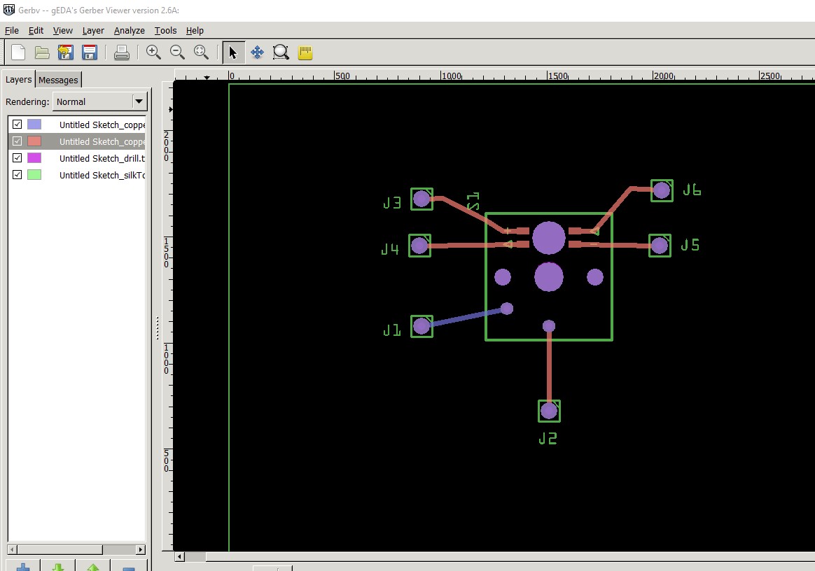
This I think does what you want although most views have changed slightly. Breadboard changed to align the pins (at least mostly!) on 0.1in boundaries. Schematic is a complete replacement generated from the Inkscape schematic extension to meet the graphics standards. PCB has corrections for the noconns and the pads and layer layout and the fzp has the changes needed to support that. The layers in pcb are changed to the standard copper1 with copper0 inside it so by default the SMD pads are on the top layer. To put the SMD pads on the bottom layer, you either need to move the part to the bottom of the board (which will move the holes!) or interchange copper1 and copper0 again in the pcb svg. This is the gerber files (displayed in gerbv) for the new part in the default top layer position
This is only the drill layer (showing only the holes)

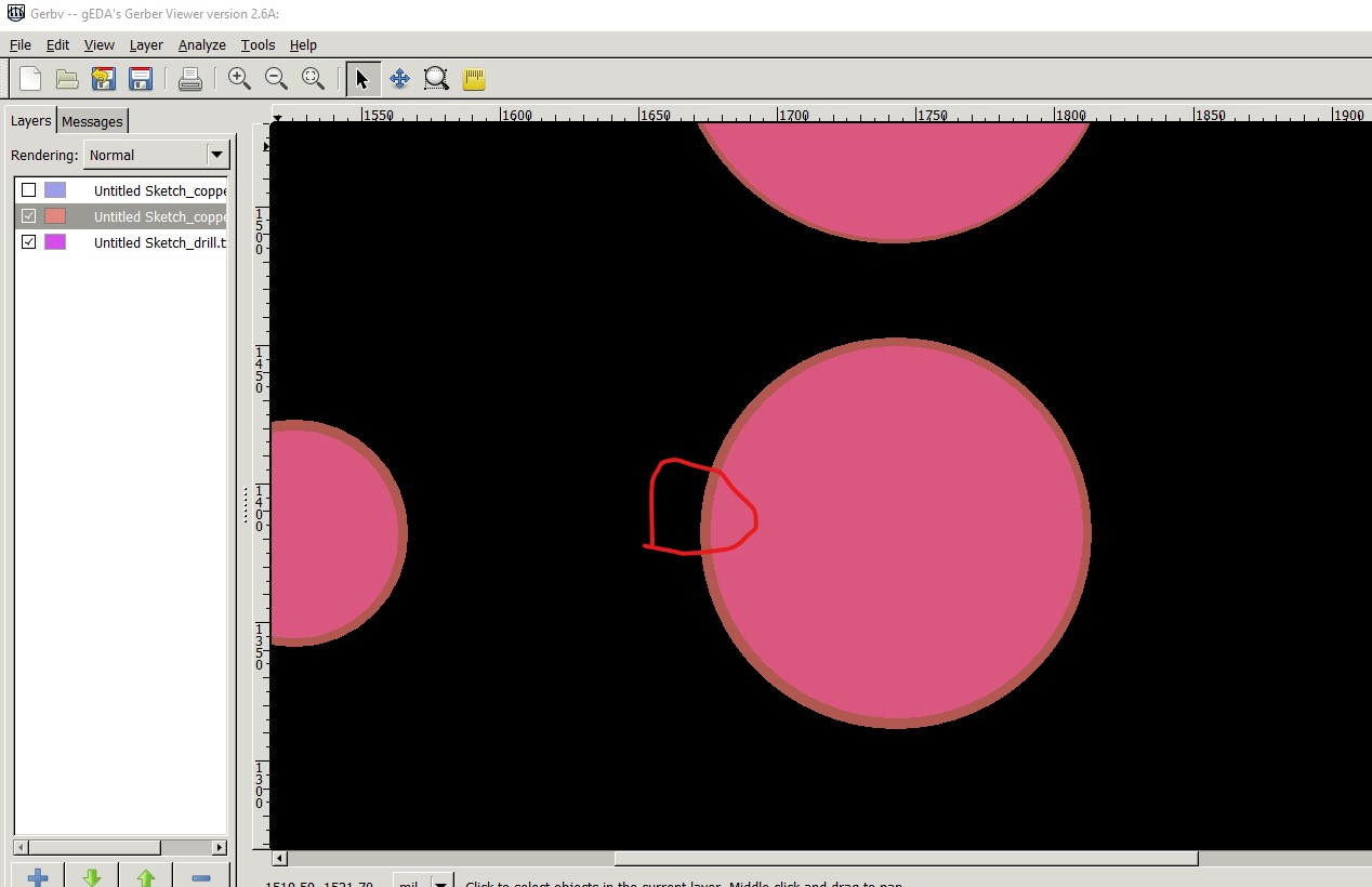
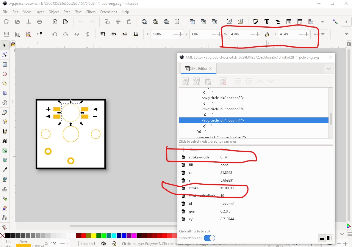
this is the original part (where the nonconns have a strokewidth and thus generate a presumably unwanted copper surround on the holes circled in red here)
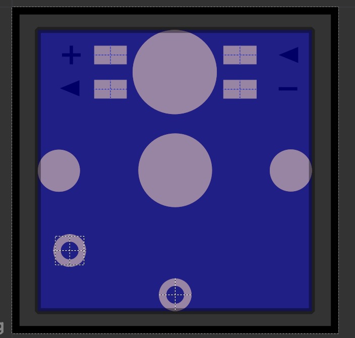
This is the pcb (default on the left, bottom of board on the right) in Fritzing
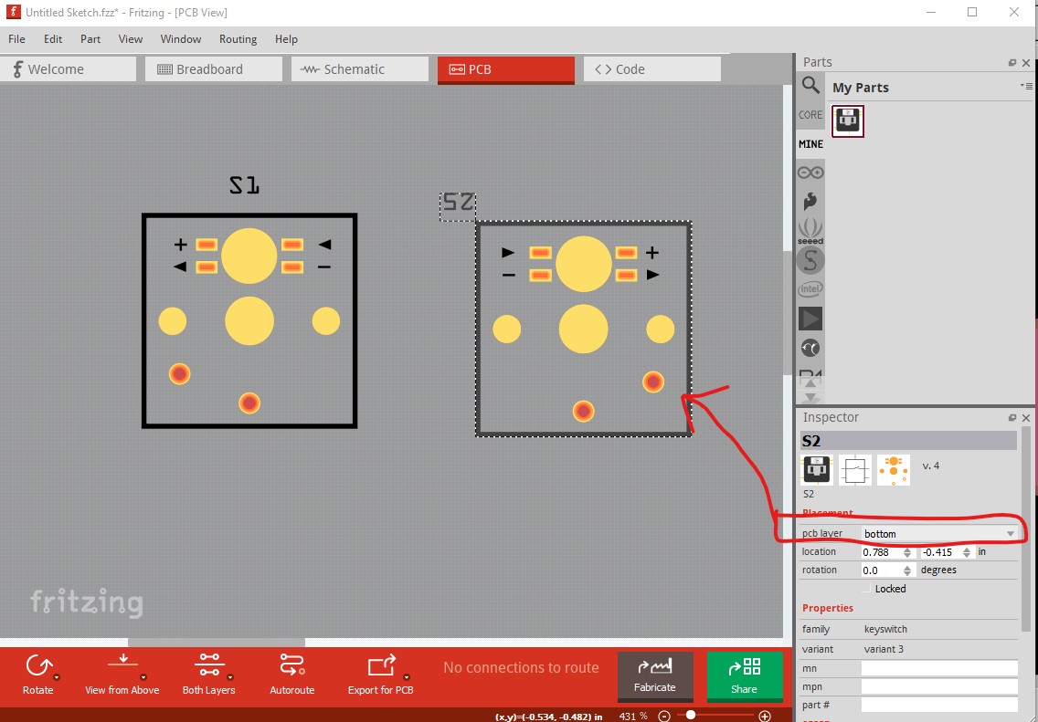
note the connector holes have moved as the switch is now on the bottom of the board. The gerbv output of the copper bottom layer which is correct, no pads on the left switch (they are on the top) and pads on the right as the switch is on the bottom of the board.
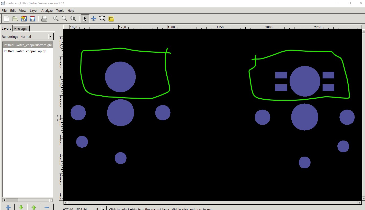
the copper top view is slightly wrong (probably because of the mix of SMD and through hole in the same part!)
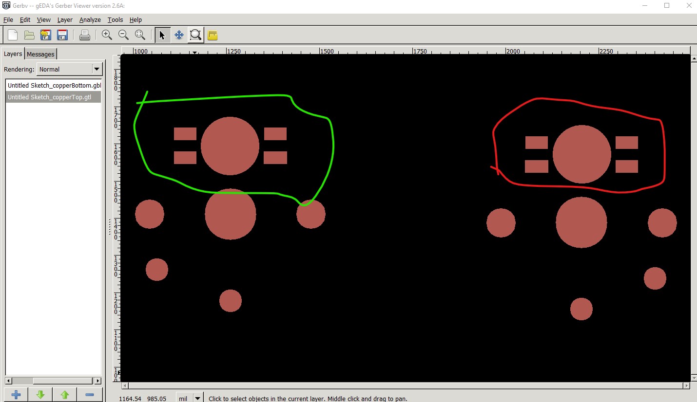
here the bottom of the board has unwanted pads on the top copper layer. It would still be useful to see a data sheet for this device both to add a description to the part and to check that the part is actually correct!
Peter
Thank you so much @vanepp for the response and the work to fix the part!
I mashed up two parts (to avoid possible misalignment issues when making a PCB layout) The LEDs are SK6812MINI-E https://cdn-shop.adafruit.com/product-files/4960/4960_SK6812MINI-E_REV02_EN.pdf and the switches are PG1350 https://cdn-shop.adafruit.com/product-files/5114/5114_CPG135001D03.pdf
The LEDs are “reverse mount” and are meant to be soldered to the bottom of the board with a cutout for the LED. I couldn’t get a rectangular noconn to work, so i went with a 4mm hole.
You mentioned the noconns being improperly defined, I’d love to know where I went wrong with those. When i made them with stroke-width=“0.0” they didn’t seem to work as holes and instead turned into undrilled copper pads – if I recall correctly, I went through a LOT of iterations of things ![]() I’ll study your part to see how it’s meant to be done.
I’ll study your part to see how it’s meant to be done.
I’ll give the fixed part a go, but with the copper0 above copper1 again.
Quick additional question: how can I select the four pads in the Parts Editor when some silkscreen rectangle is blocking them? This is with my cursor hovering over one of the rectangular LED pads.
I had to move my silkscreen layer below the copper layers in my SVG to prevent this. I’m running Fritzing 0.9.10 on mac os Ventura 13.1.
OK, so it looks like you need to swap copper 0 and copper1 in my pcb svg to get the placement right. In the original pcb svg, by the time the nonconns made the svg they had a stroke width (which causes the copper ring):
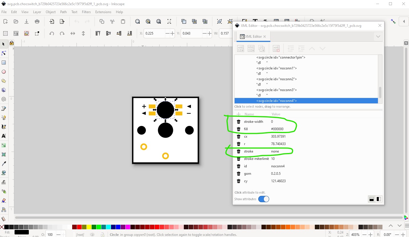
a Fritzing nonconn should have 0 stroke-width and a black fill to drill only the hole like this (I think it actually creates the copper pad as well, but the copper gets removed in the drill stage.)
How I make parts is detailed in this tutorial (which edits the underlying files directly)
old_grey uses parts editor in his tutorials though
(both of these apply to 0.9.10 as well, many of the others are for older versions.) I rarely use parts editor (it is as of 0.9.10 incomplete, I believe it is being worked on) and will likely break with this non standard layout (a mixed through hole and SMD part will likely confuse it!)
It will select the through hole pad on connector0 from the window
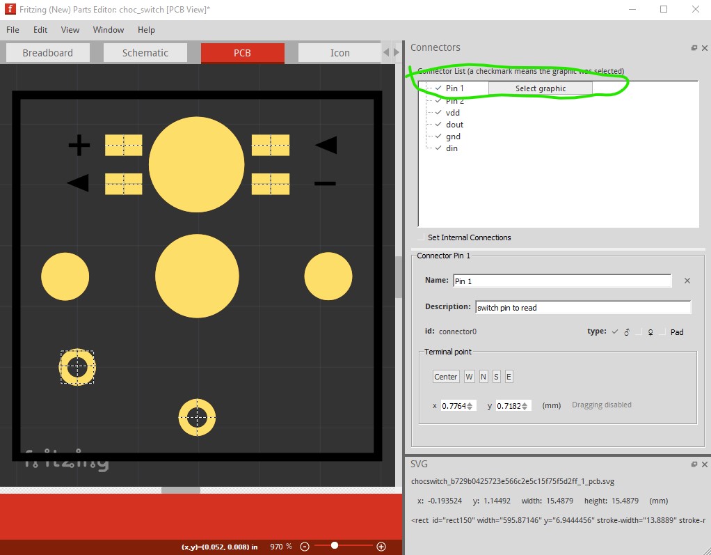
but can’t seem to select the pads only on copper1 unless I click on the label in the connector window (which won’t work I expect if you don’t have the connectors defined.) I expect but don’t know for sure that this is because of the non standard layout of the part.
edit: Slots can not be created in parts, you need to load a custom cutout svg (which are typically difficult to make!) for the entire board which means the slots for all the keys would need to be done in the svg and then the parts moved over them which is a major pain. The usual solution is to use a hole as you have done and that will be much easier in this case. You might want to add a description field to the .fzp file (or description in parts editor) explaining this par is really two parts connected together and give the urls to the individual parts so someone coming on the part knows there isn’t a single part that will do this out there somewhere and can get the two parts and make the part. This should create fairly cool keyboards!
Peter