Bonjour.
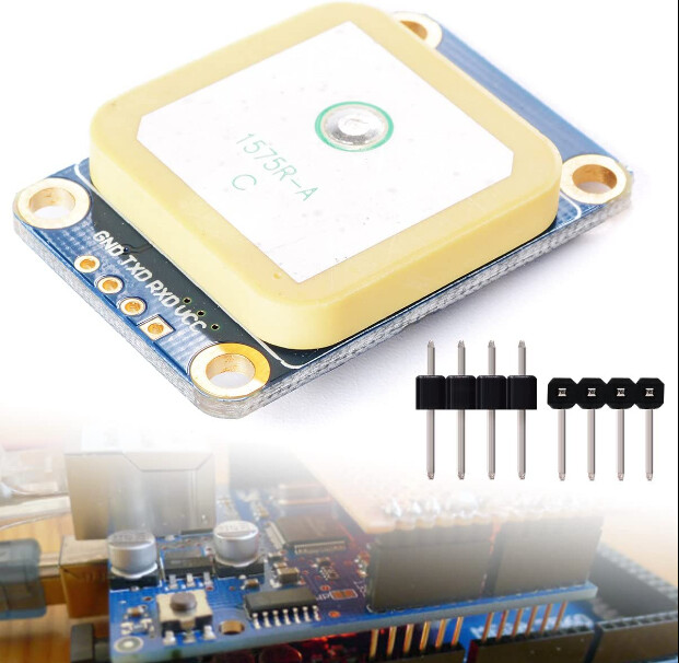
Un petit partage d’un module GPS NEO-6M avec antenne incorporé(collée dessous le circuit).
GY-NEO6MV2.fzpz (13.6 KB)
(mise a jour des connecteurs dans la vue schématique).
Bonjour.
Un petit partage d’un module GPS NEO-6M avec antenne incorporé(collée dessous le circuit).
GY-NEO6MV2.fzpz (13.6 KB)
(mise a jour des connecteurs dans la vue schématique).
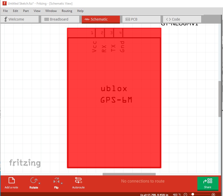
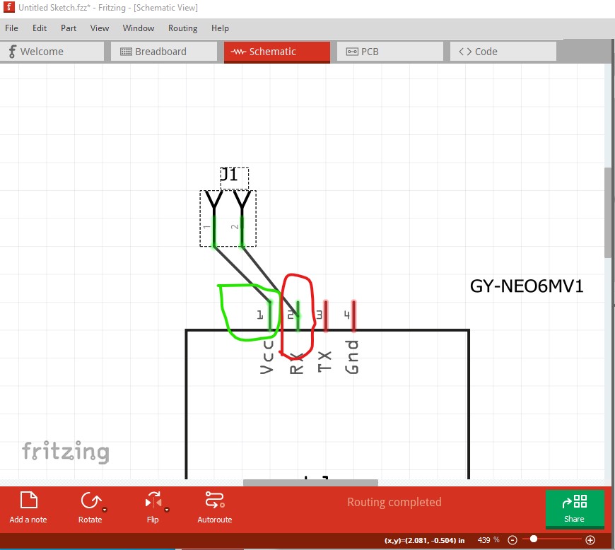
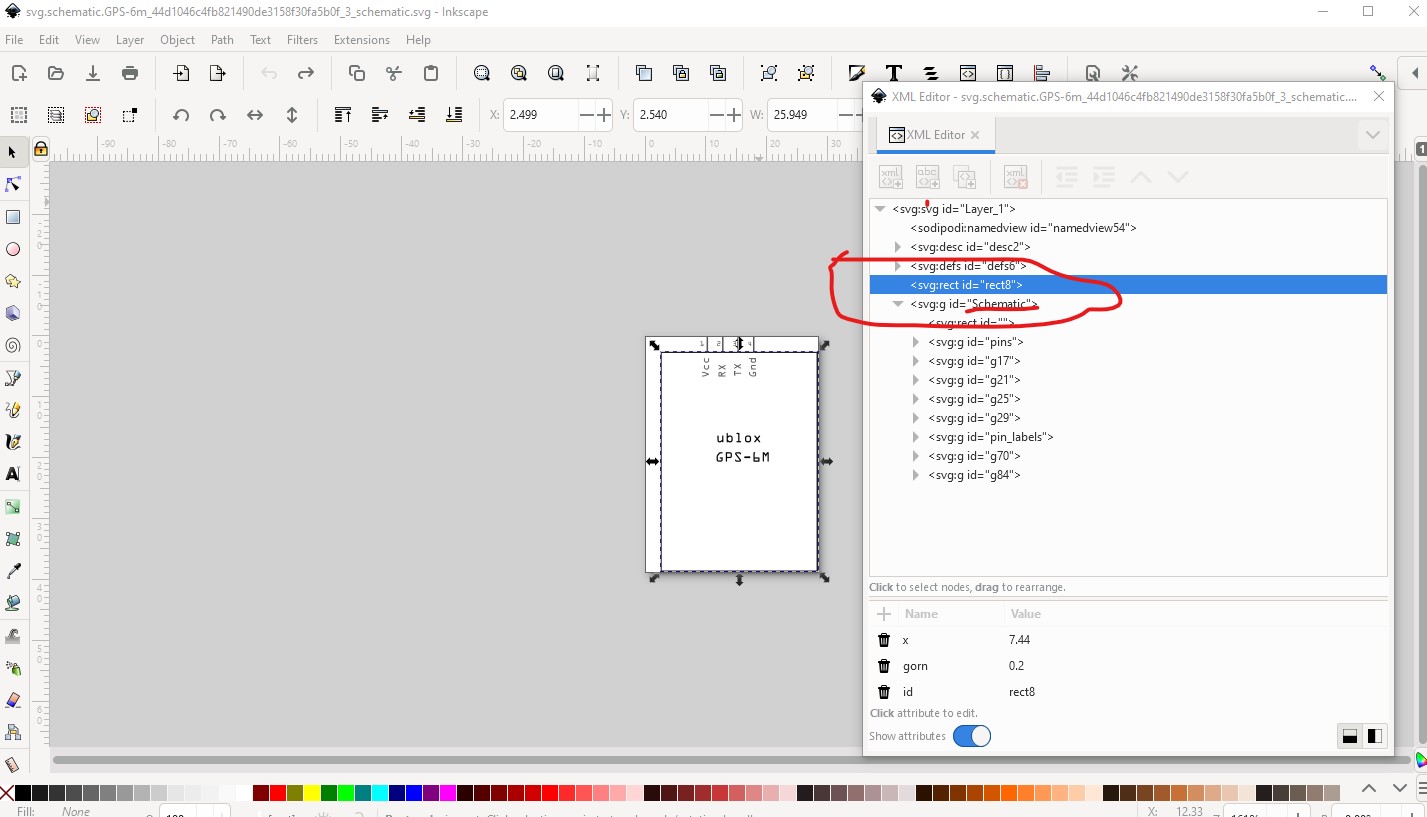
A number of problems,
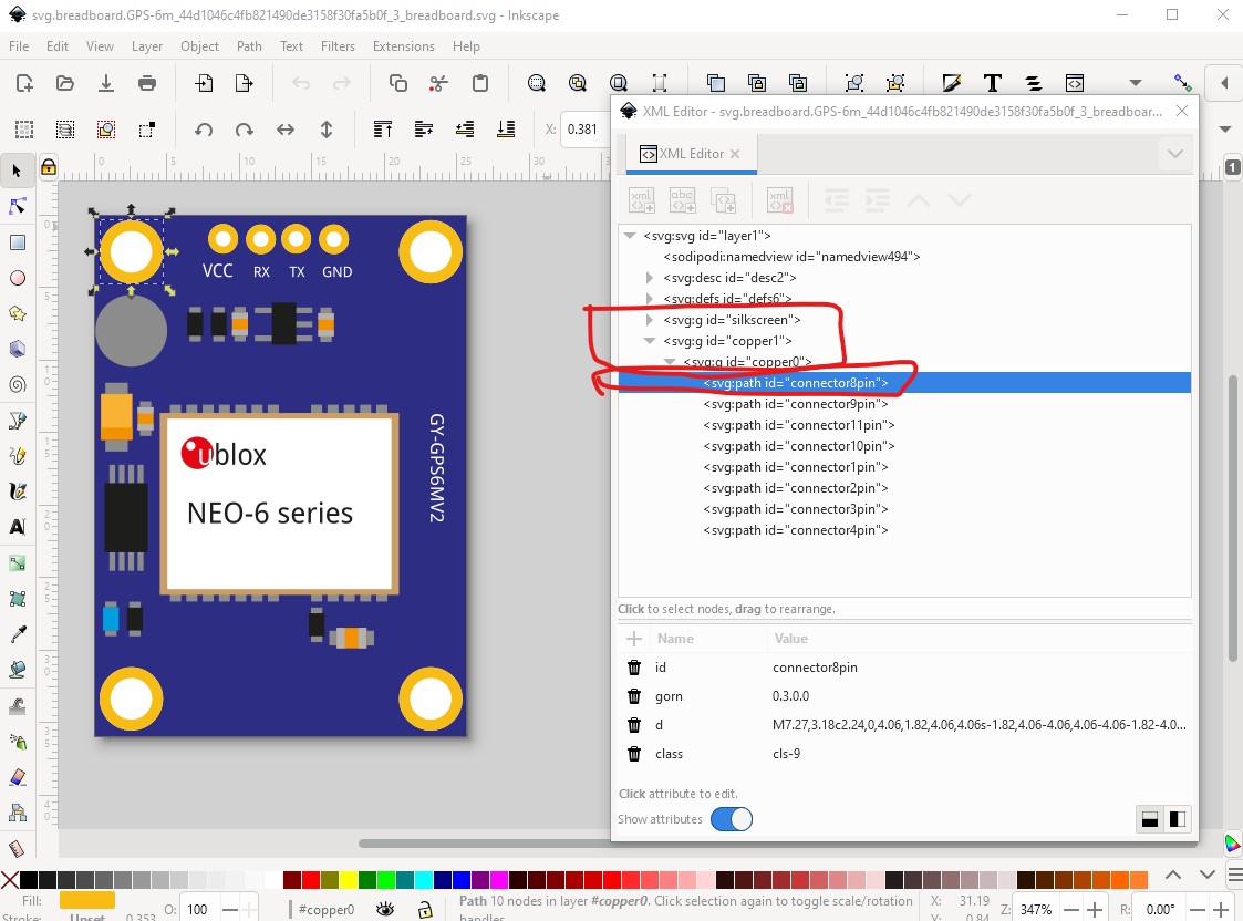
there are no connections defined in schematic thus the red rectangle. The pads in pcb should be circles not paths and are too large (the holes should be 0.038in for 0.1in headers not 0.067in
; NON-PLATED HOLES START AT T1
; THROUGH (PLATED) HOLES START AT T100
M48
INCH
T100C0.066941
%
T100
X018116Y017765
X017092Y017777
X016134Y017763
X015111Y017777
T00
M30
the schematic layerId has a capital S (Schematic rather than schematic) and thus doesn’t match the fzp file and won’t export as an image. There are bus definitions that don’t have pins in the fzp file as well. These two tutorials (which apply to current Fritzing versions) may help:
Peter
Bonjour. Je viens d’éditer le parts. J’avais en effet oublié la partie de marquage des pins dans la vue schématique, et aussi de bien vérifier les numéro des pins.
Par contre pour les autres explications, je suis navré, je ne comprend pas. les pins de la vue schématique, sont bien espacées de 0.1in (j’utilise une grille sous illustrator sans subdivisons).
![]()
The schematic pin problem isn’t an svg spacing issue but rather a schematic svg vs fzp file issue. The fzp file looks like this:
<connector type="male" name="Vcc" id="connector1">
 <description>Vcc</description>
 <views>
  <breadboardView>
   <p svgId="connector1pin" layer="breadboard"/>
  </breadboardView>
  <schematicView>
   <p svgId="connector1pin" layer="schematic"/>
  </schematicView>
  <pcbView>
   <p svgId="connector1pin" layer="copper0"/>
   <p svgId="connector1pin" layer="copper1"/>
  </pcbView>
 </views>
</connector>
it needs to look like this:
<connector type="male" name="Vcc" id="connector1">
 <description>Vcc</description>
 <views>
  <breadboardView>
   <p svgId="connector1pin" layer="breadboard"/>
  </breadboardView>
  <schematicView>
   <p svgId="connector1pin" layer="schematic" terminalId="connector1terminal"/>
  </schematicView>
  <pcbView>
   <p svgId="connector1pin" layer="copper0"/>
   <p svgId="connector1pin" layer="copper1"/>
  </pcbView>
 </views>
</connector>
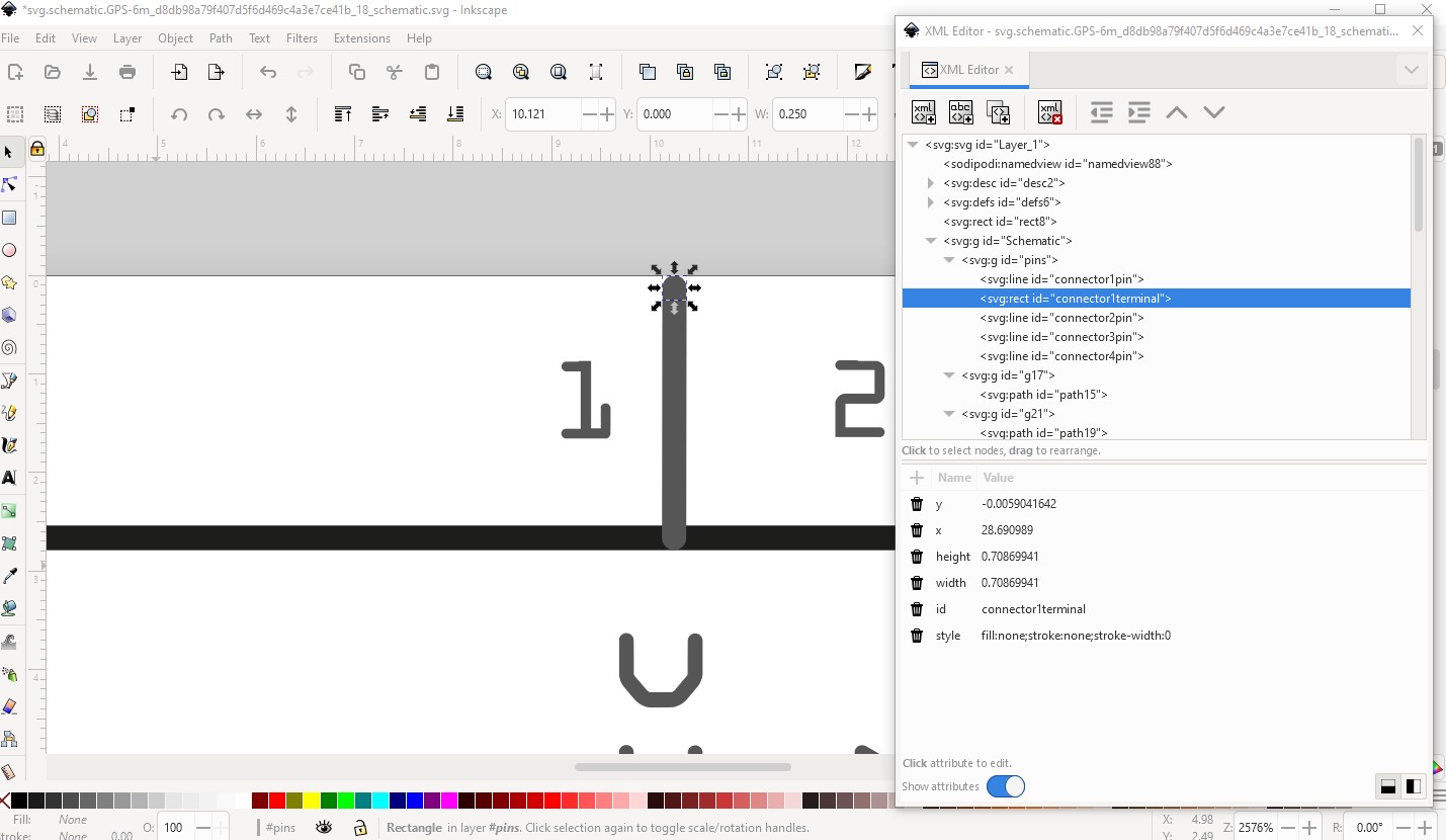
to define a terminalId in schematic. Then the schematic svg needs to add a terminalId like this (in Inkscape rather than Illustrator but the result should be the same!)
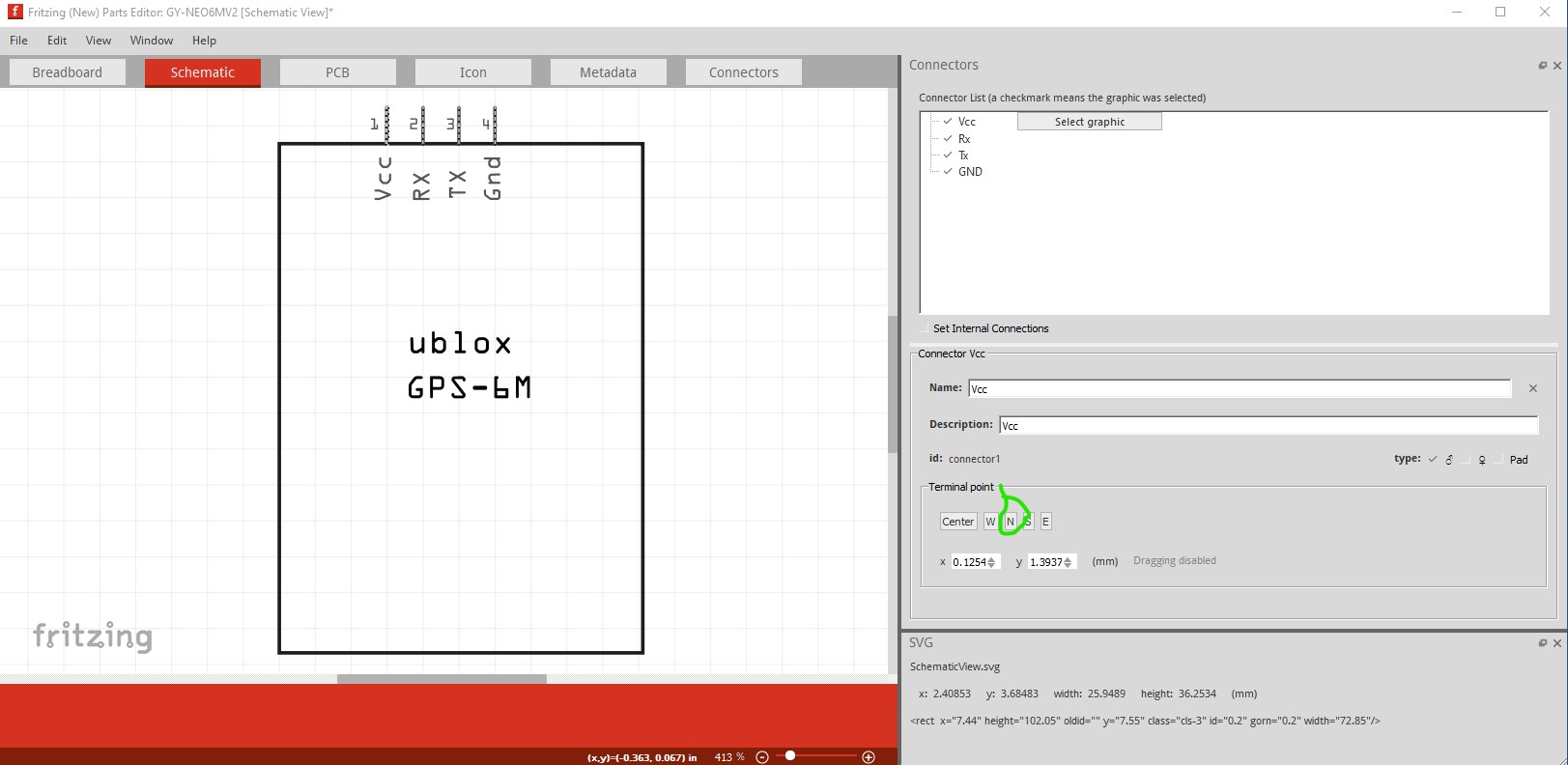
the terminalId is a rectangle the same height and width as the line that is the pin at the top of the line that is the pin. If you are using the parts editor (which I usually do not) the same effect can be done like this:
by clicking on the north button, the parts editor will modify the fzp file to add the terminalId and modify the svg to add the rectangle and the terminal definition. The result is that the wire will then connect to the end of the pin as it should like this:
here I corrected pin1 but not pin2. As you see the end of the pin is now on the 0.1 grid line (because of the terminalId) and the wire connects to the top of the pin rather than the middle as pin2 does. Here is a copy of the modified part for reference.
GY-NEO6MV2.fzpz (13.7 KB)
Peter
Mise à jour de la vue schématique suivant les recommandation de Peter. Merci à lui ![]()
GY-NEO6MV2_v2.fzpz (14.2 KB)
Still a number of problems. FritzingCheckPart.py has these complaints:
Error 53: File
‘part.GPS-6m_ae2a5eb80f3bf050b50b26dc1b48580f_1.fzp.bak’
At line 132
Bus nodeMember connector19 does’t exist
Error 53: File
‘part.GPS-6m_ae2a5eb80f3bf050b50b26dc1b48580f_1.fzp.bak’
At line 133
Bus nodeMember connector22 does’t exist
Error 64: File
‘part.GPS-6m_ae2a5eb80f3bf050b50b26dc1b48580f_1.fzp.bak’
Connector0 doesn’t exist when it must to stay in sequence
Error 69: File
‘svg.breadboard.GPS-6m_44d1046c4fb821490de3158f30fa5b0f_3_breadboard.svg.bak’
At line 80
Found a drawing element before a layerId (or no layerId)
Error 69: File
‘svg.schematic.GPS-6m_44d1046c4fb821490de3158f30fa5b0f_3_schematic.svg.bak’
At line 38
Found a drawing element before a layerId (or no layerId)
Error 74: File
‘svg.pcb.GPS-6m_44d1046c4fb821490de3158f30fa5b0f_3_pcb.svg.bak’
At line 19
Connector connector1pin has no radius no hole will be generated
Error 74: File
‘svg.pcb.GPS-6m_44d1046c4fb821490de3158f30fa5b0f_3_pcb.svg.bak’
At line 20
Connector connector2pin has no radius no hole will be generated
Error 74: File
‘svg.pcb.GPS-6m_44d1046c4fb821490de3158f30fa5b0f_3_pcb.svg.bak’
At line 21
Connector connector3pin has no radius no hole will be generated
Error 74: File
‘svg.pcb.GPS-6m_44d1046c4fb821490de3158f30fa5b0f_3_pcb.svg.bak’
At line 22
Connector connector4pin has no radius no hole will be generated
the last 4 are not entirely correct as the paths do generate holes but they are undesirable as they are hard to change. Starting with breadboard here are the problems and their solution:
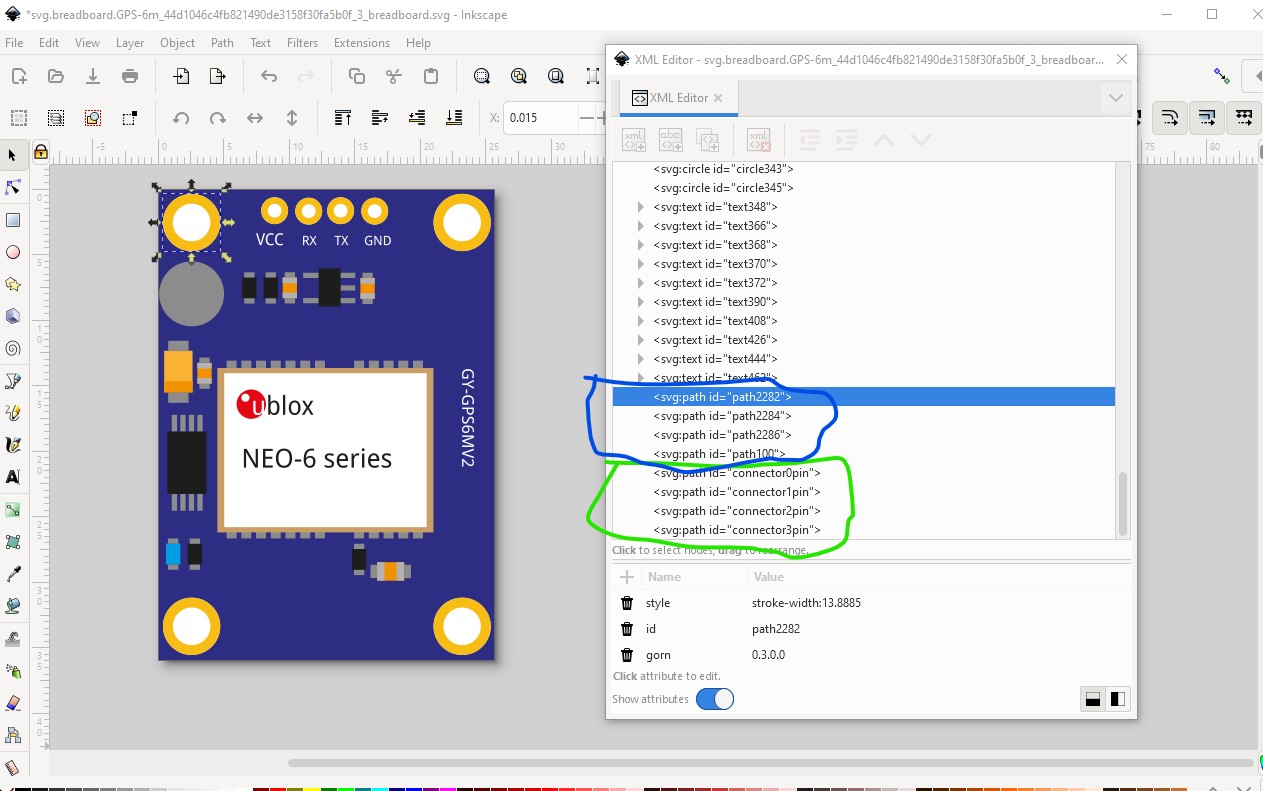
The groups are incorrect. There should be a single group with the group name breadboard. The mounting holes should not have connector numbers as they aren’t connectors, and the pin numbers should start at 0 not 1.
so change the mounting hole names from connector to path and renumber the connectors from 0 (we will also need to change the .fzp file because of this!)
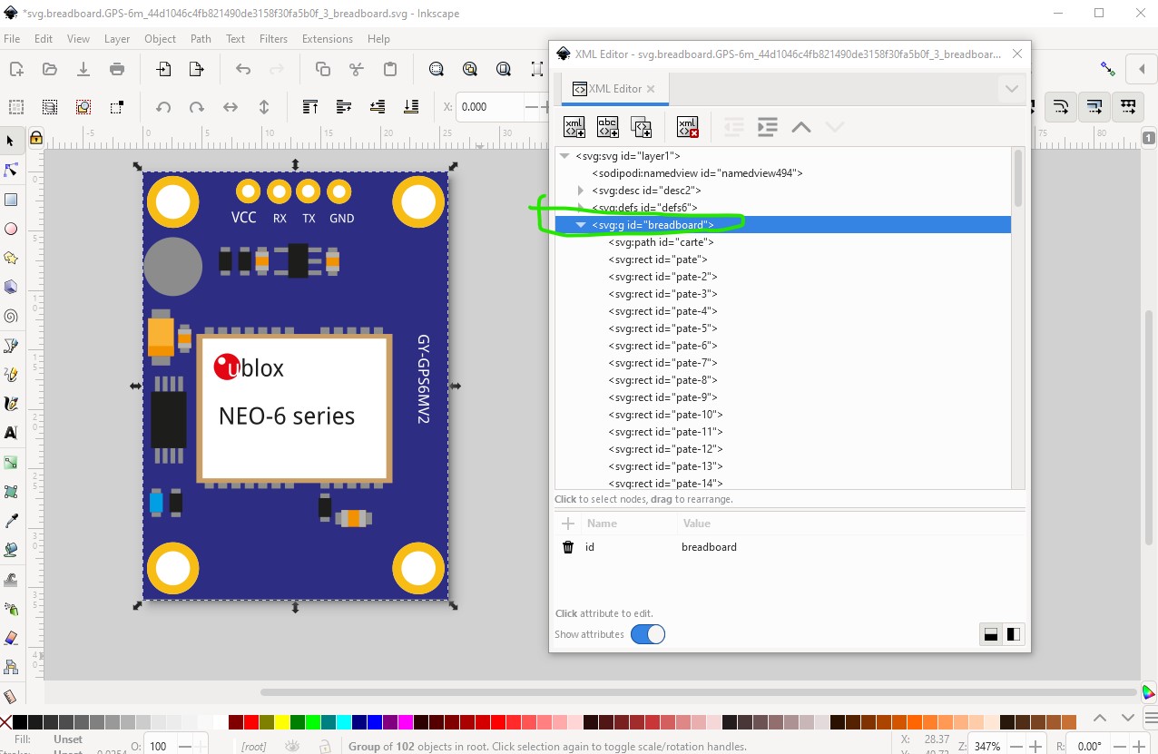
then regroup the entire drawing and name the group breadboard to set the correct layerId (which in turn will cause the part to export as an image which it will not if the layerId is wrong!) That completes breadboard so on to schematic.
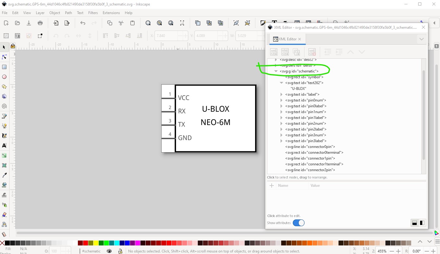
Here the outer rectangle is outside the layerId (and thus won’t appear in an image) and the layerId is incorrect (“Schematic” when the fzp file specifies “schematic”) and thus there won’t be a layerId. Schematic is also undesirably large so I replaced it with one created by the Inkscape Fritzing schematic extension (which generates schematics which meet the graphics standards document) like this
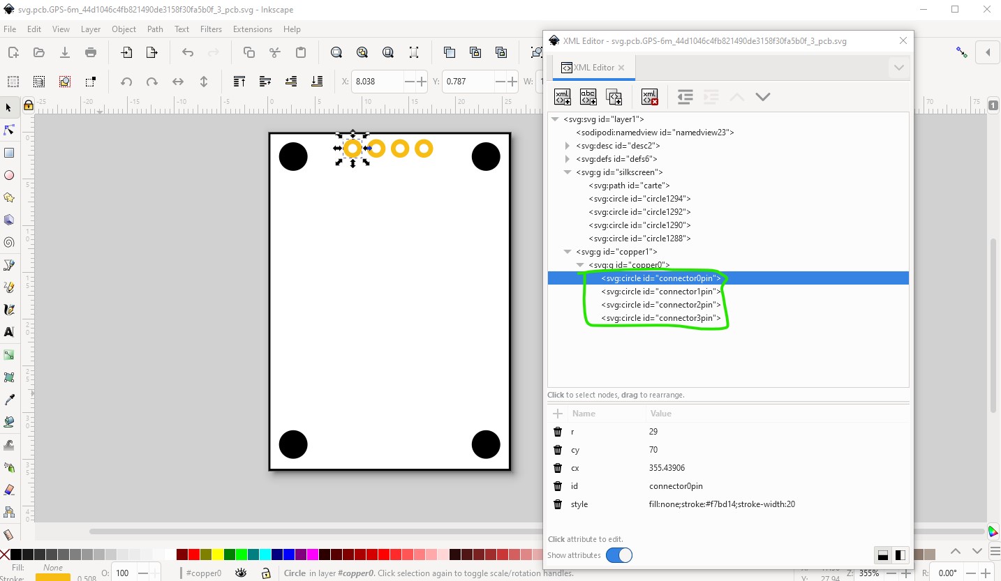
Now on to pcb
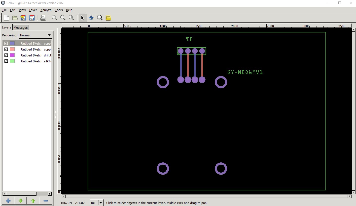
Here I copied the breadboard svg in to the current pcb to use to create a better pcb layout. The original pcb lacks a silkscreen layer, has paths for the pads (which is undesirable as it is hard to change the hole size.) So I deleted the original pcb entirely and started from the breadboard. I modified the path to produce a rectangle that is the edge of the board in silkscreen, then changed the mounting holes to circles only in silkscreen (they won’t be drilled!) If the user wants mounting holes drilled they can drag a hole over the circle in silkscreen in the sketch to drill the holes. If they don’t want holes they don’t have to modify the part to remove them. I then replaced the paths for the pads with circles set to have a hole size of 0.038in suitable for a standard 0.1in header and renumbered the pins starting at 0 to produce this final pcb:
If you want to change the hole size here it is only necessary to adjust the radius value to give the new hole size. All these changes are in this new part
GY-NEO6MV2_v2-fixed.fzpz (7.5 KB)
which generates 0.038in holes in the gerber output
; NON-PLATED HOLES START AT T1
; THROUGH (PLATED) HOLES START AT T100
M48
INCH
T100C0.038000
%
T100
X014106Y015777
X016106Y015777
X015111Y018777
X015106Y015777
X013111Y018777
X013111Y015777
X016111Y018777
X014111Y018777
T00
M30
which generates a proper silkscreen in the geber output
as opposed to the original part which lacks the silkscreen and has large holes (0.066in rather than 0.038)
; NON-PLATED HOLES START AT T1
; THROUGH (PLATED) HOLES START AT T100
M48
INCH
T100C0.066941
T101C0.038000
%
T100
X014997Y015538
X014038Y015524
X013015Y015538
X016020Y015525
T101
X015015Y019538
X014015Y019538
X013015Y019538
X016015Y019538
T00
M30
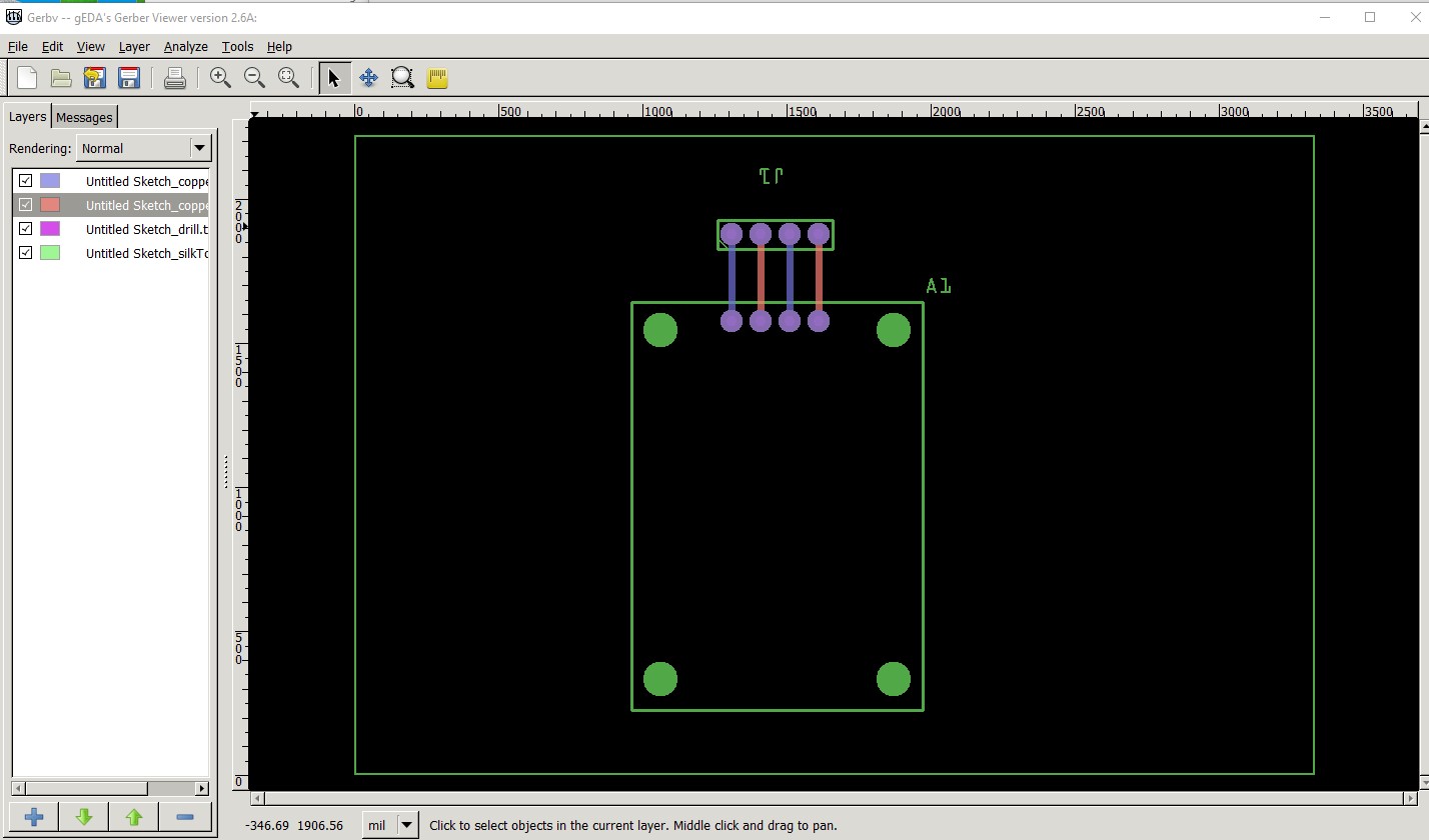
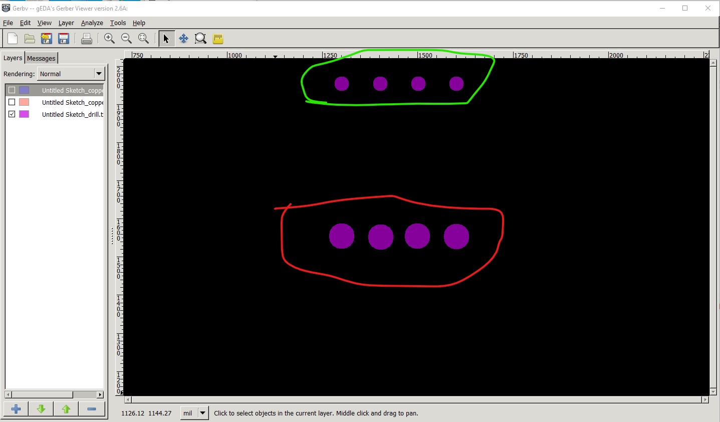
the standard header is circled in green and the large holes in pcb are circled in red.
The mounting holes are not drilled but do appear on the copper layer (which is likely undesirable!)
and there is no silkscreen outline of the board (because there is no silkscreen layer!) Hope this helps!
Peter