So I did all the connections on the breadboard view and so far it looks fine. The problem is that the clone board I am trying to model has multiple ground, reset, and vcc pins that are all connected but I have no idea how to connect them to the same node on the schematic.
Your best bet is to upload the sketch (the .fzz file, upload is 7th icon from the left on the reply menu) so we can see what you are trying to do and help you.
Peter
Arduino 32Mhz Mini clone.fzpz (16.9 KB)
Ah, it becomes clearer. You are trying to modify a part rather than a sketch. This set of tutorials is how I do this task without using parts editor by editing the underlying files instead.
This series of video tutorials by Old_Grey covers parts editor and other topics.
As to your specific question here is how you do it using Inkscape (it should be similar if you are using another svg editor)
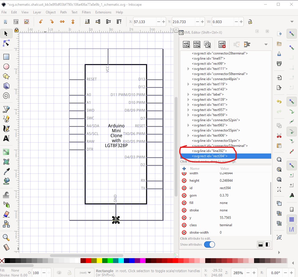
First you need to associate the connectorxpin connection with its associated terminalId, they are wrong in these two images. I chose this particular pin pair because the terminalId is the correct one for the ground pin that you need to dup to make this work.
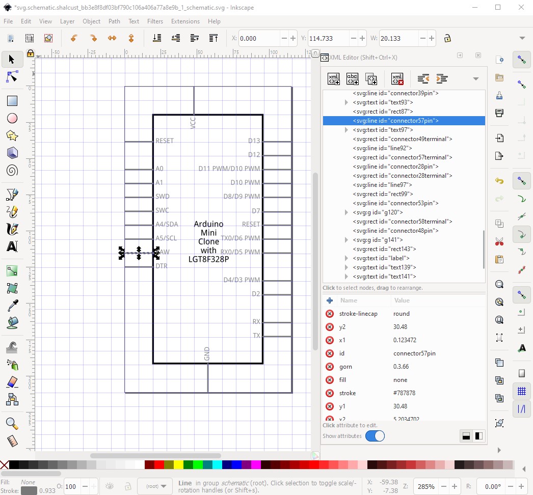
First I ungrouped the entire svg to make life easier (at the end of it all you need to do an edit–>select all and then group and set the id to schematic to set the correct layerId.) Then I moved connector53pin and
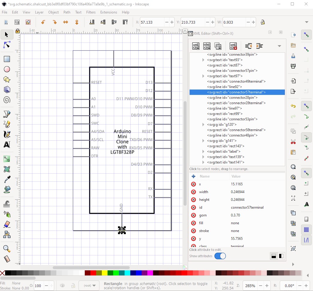
connector57terminal (renaming it to connector53terminal as it should be) to the bottom of the xml editor window.
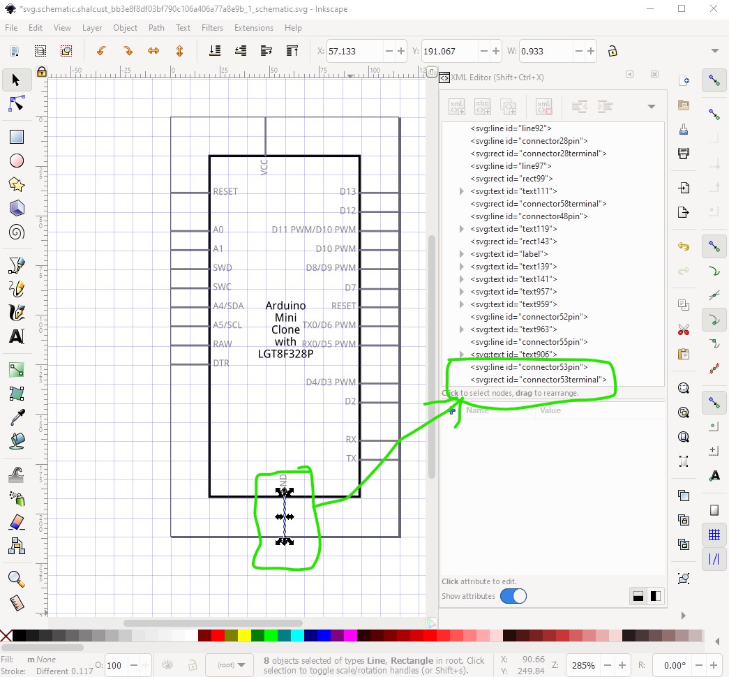
Then I selected both the pin and terminal and duplicated them which has an unexpected result:
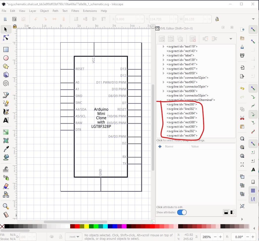
there are already a number of pins overlaid on the ground pin (probably from whatever you cloned this from.) So delete all of them except for one pin and one terminal like this:
now switch to the breadboard svg and find connector53pin (which is already correctly present in schematic) as a reference point.
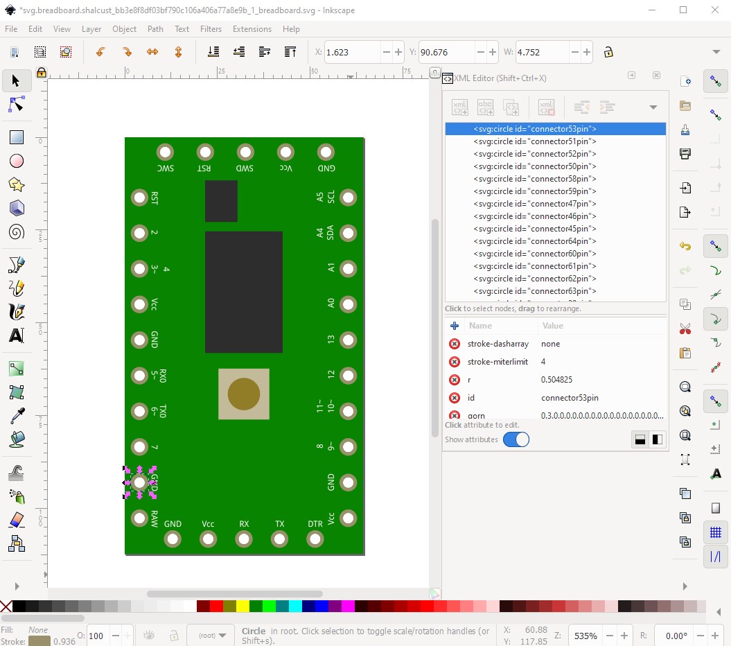
Now select one of the other ground pins connector56 in this case) to add to schematic.
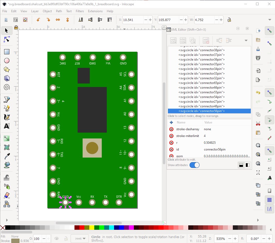
and change the id on the line to connector56pin and the rectangle to connector56terminal which overlays another ground pin on the same place in schematic. Note that once you have done all this you then need to adjust the bus configuration (internal connetions in parts editor) to place all the associated pins overlaid on top of each other in the same bus.

Do the same thing for any further connections needing to share a single pin.
Peter
1 Like
Have you seen 2.1 Part file format? The section on “buses” (search for “internal connections”) is what applies for this.
Each pin has a connector in the fzp meta data. For each connector, the svgId information links to the id values in the svg files. A bus entry tells Fritzing that all of the referenced connector ids are internally connected together. In all views. The “trick” for schematic is one of 2 things. You can mark all but one of the connectors as “hybrid”, and/or you can stack the connector and terminal id svg graphics on top of each other, so that they are at the same location in the graphics. Hybrid seems to be the “correct” way, but I have not gotten clean instructions to make it work in all scenarios. The best result I have gotten is to mark the schematic connector entries as hybrid=“yes” for all but one of the entries of a bussed group, position the terminalId and svgId svg schematic elements at exactly the same coordinates as the final entry of the group, and make the hybrid elements invisible by marking them as stroke="none" fill="none". That seems to look and function as desired.
I would have “expected” that with the meta data marked as hybrid, the schematic svg file would not even need to contain the svgid and terminal id for the connector. But that does not work.