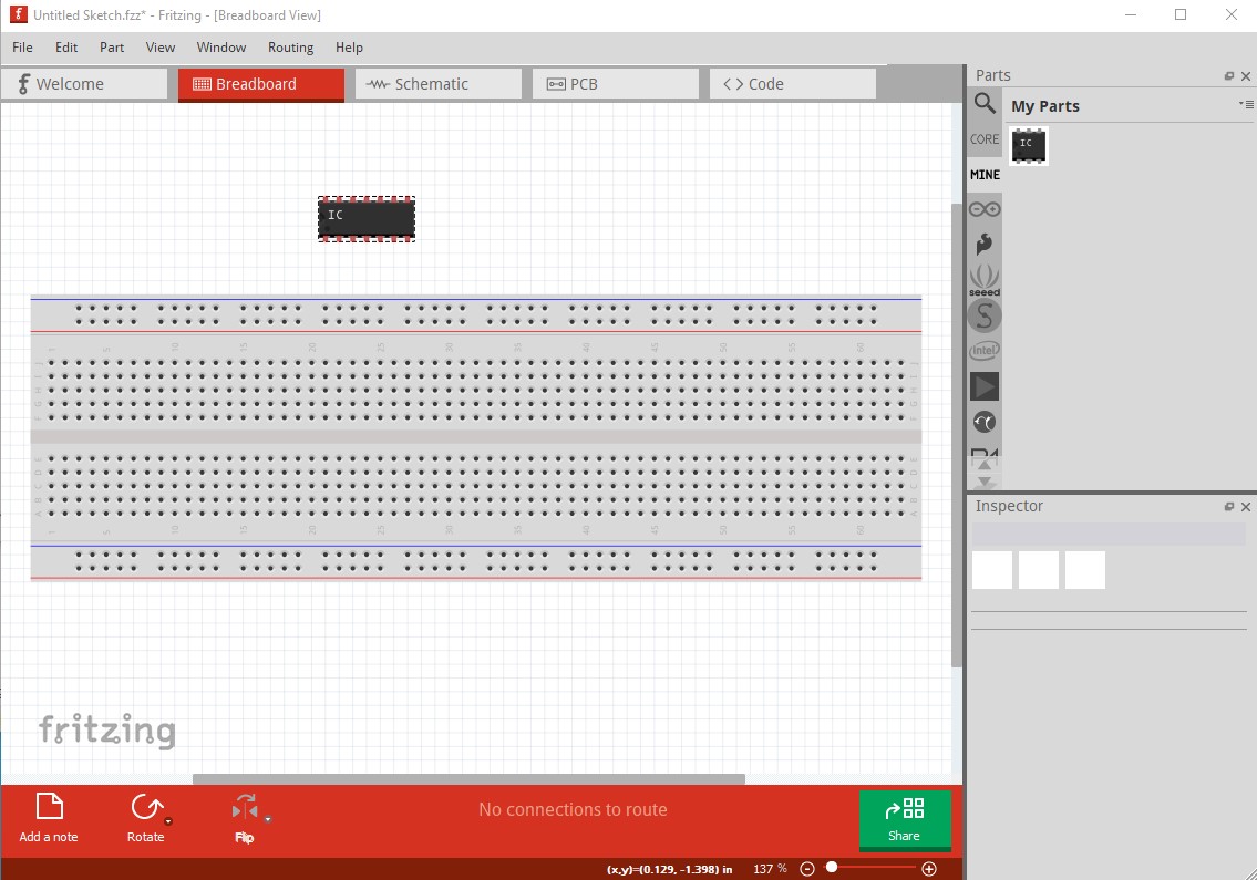
I have downloaded chips from here
They are almost what I want but the tops of the chips in the breadboard view show just ‘IC’ can I change this to 47ls04 etc?
I have downloaded chips from here
They are almost what I want but the tops of the chips in the breadboard view show just ‘IC’ can I change this to 47ls04 etc?
Not without creating a new part, which is really just creating a new breadboard svg with the text you want.
My own preference is for parts without any ‘on chip’ labelling at all. That way, if a label is needed, it can be added to the sketch using the text part provided by Fritzing.
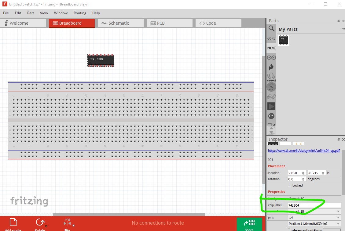
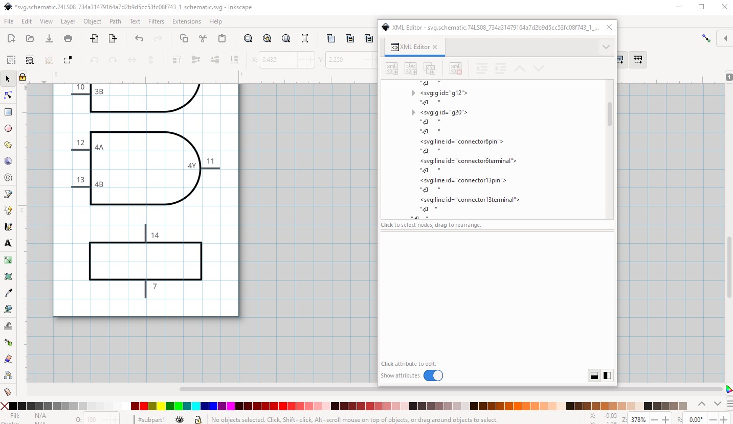
In this case you can change the chip label field in Inspector (but apparently only after saving the mine parts bin due to a Fritzing bug) like this:
by changing the chip label field in Inspector (circled in green) the chip will be relabeled like this:
Peter
Thank you microMerlin, but I think I would like to see the name of the chip in the breadboard view.
vanepp, I changed the label and the chip showed up as, in my case, 74ls04 on the breadboard view.
I would also like to alter the pins so that if I hover over one I get its function, i.e. pin 7 is gnd. I can do this by opening the parts editor and altering the pin names there, this then saves and I get the pin names in future chips I drag onto the breadboard, job done.
I can go to Metadata in the editor and alter the label to 74ls04 but it does not show on the chip.
I assume the chip is designed in inkscape or some similar package, is it possible to move it back into inkscape, alter it to the desired label and then replace the chip in fritzing?
Alternatively I have found a similar download for the chips but it does show the 74ls04 0n the chip but the schematic just shows a box with 14 pins instead of the separate gates, might it be possible to combine the properties of both these files to give me what I want?
I am now going to see if I can find another importable chip that also gives me what I want, the chip with a name on in breadboard, the legs that tell you what they do when hovered over them and separate gates in schematic.
You need the chip label in properties (or in the fzp file) not the label (which is U for IC and is the label of the chip.) Here I unzipped the fzpz file to get the fzp and the 4 svgs then edited
part.74LS04_980f2b69f7522fd48bea7098d8006ef4_2.fzp
for the label change from:
<properties>
  <property name="family">Generic IC</property>
  <property name="package">DIP (Dual Inline) [THT]</property>
  <property name="pins">14</property>
  <property name="pin spacing">300mil</property>
  <property name="chip label">IC</property>
  <property name="hole size"/>
to
<properties>
  <property name="family">74LS04</property>
  <property name="package">DIP (Dual Inline) [THT]</property>
  <property name="pins">14</property>
  <property name="pin spacing">300mil</property>
  <property name="chip label">74LS04</property>
  <property name="hole size"/>
here I also changed the family property from Generic IC to 74ls04. If it remains Generic IC the parts factory will rearrange the part if you change the chip type (which I typically don’t want, you may or may not want to swap parts though.) Note this is a schematic subpart part so the individual gates in schematic will move around independently, so be careful if you modify the schematic svg because its format is important. The pin names are also changed in the fzp file in the description property of the connector like this from:
<connector name="pin1" id="connector0" type="male">
  <description>pin 1</description>
to
<connector name="pin1" id="connector0" type="male">
  <description>IN-A</description>
the description field shows up in the data displayed when you hover over the pin. Replacing this:
<iconView>
  <layers image="icon/74LS04_1301646018940d479352cc70054d637c_1_icon.svg">
    <layer layerId="icon"/>
  </layers>
</iconView>
with this:
<iconView>
  <layers image="breadboard/74LS04_1301646018940d479352cc70054d637c_1_breadboard.svg">
    <layer layerId="icon"/>
  </layers>
</iconView>
will make the icon that shows up in Inspector (the lower right window) from an 8pin chip to the correct 14pin chip as well. If I were doing this I would probably also increase the font size on the pin labels in the schematic svg (which would require an svg editor such as Inkscape) as they are currently rather small.
Like this in Inkscape
Here I changed pin 1 from a font-size of 2.8346 to 5 to make it slightly larger (there are actually proper sizes but the scale of this svg is non standard and I’m to lazy to convert it!) You then need to save the svg as plain svg and after exiting Inkscape either use a text editor to remove the px from all the font-sizes or process the part through FritzingCheckPart.py which will do that automatically. These two tuturials apply to the current version of Fritzing (and mine is how I make parts typically not using the parts editor!)
If anything is unclear feel free to ask!
Peter
Thank you so much for all that Peter.
I will take a while to go through it and then get back to you.
Bob.
Hi Peter,
I am sorry for the delay, I don’t get much time to sit down and work through this.
I succeeded in altering the 74ls08 files as you indicated so that the pin numbers are larger and the chip has its name on the top of it plus a few other slight alterations by altering the files directly.
I also did this for a few other chips.
I then succeeded in making a new bin with a box in the left edge of the parts section , a white box with a large ‘IC’s’ in it.
I thought I had moved all my chips by dragging and dropping them when in fact I just copied them.
As a last clean up I deleted the chips from the original bin and finished up deleting hours and hours of work as it deleted the files I had just altered.
I have remade some of the files, zipped them as fzpz’s and saved them elsewhere. I now have 74ls04 INV, 74ls08 AND, 74ls32 OR.
I am now looking at replacing new ones I download, such as 74ls00 that have just a box with wires in the schematic as opposed to sub units, with sub unit ones that I alter in the schematic svg file (74ls00 is a NAND file where 74ls08 is an AND file so I just need to add the small circle)
The SVG files (is it HTML?) contain a lot of <g>'s. They are used to group SVG files but does it need so many?
I notice some items have a description that appears when you hover over them? I am not sure how that happens but that is another thing I will look at.
I will, of course, offer them to the forum when I get them finished.
Bob.
Note you also need to add the schematic subpart section to the fzp file for this to work successfully. Without the definition in the fzp file, subparts won’t work.
It is xml which html is an offshoot I think.
For reasons unknown parts editor loves adding unneeded groups. Typically the first thing I do is either completely ungroup the svg (if there is a single master group) or Edit-select all Object->group and then ungroup the resulting single group to make an ungrouped svg. When you are finished your changes do Edit->select all, Edit->resize page to selection (which sets the start coords to 0 0) then Object->group and set the layerId (breadboard, schematic, etc) as the group name. Fritzing only cares about the layerId group the rest are optional.
That is the name and description fields in the fzp file
<connector id="connector1" name="pin2" type="male">
  <description>GND</description>
here the hover label will display “pin2” from the name field and “GND” from the description field as well as the connector number + 1 (as connectors start at 0 and pins start at 1, so connector 0 will display a 1 as the pin number. )
Peter
Hi,
I was thinking I had seen the description of the ic when I hovered over it instead of a description of the pin when I hovered over it.
I am now altering 74ls08, an AND GATE, to 74ls00, a NAND gate by adding the circles from the invertor gate 74ls04.
I decided to replace the whole of the program for the schematic of the 74ls00 with the one for the 74ls08, by copying and pasting the contents. This means the names of the files will be correct. (I know, I could have changed the name of the file but one way or the other works).
I can’t get the wording on the box of the supply sub part in the schematic to change from 74ls08 to 74ls00, is this possible from within the files or is it grabbed from an external file made in inkscape?
Thanks,
Bob.
Yes I was somewhat imprecise, if you hover over the body of the IC (not a pin) it will display the chip label field from the fzp file like this:
where IC1 is the label of the chip and IC is the chip label field (it may include the title if the chip label field isn’t present in the fzp.) Hovering over a pin gets the name and description fields from the connector in the fzp file:
You could put something like A-In in the description field to indicate what the pin is if you like.
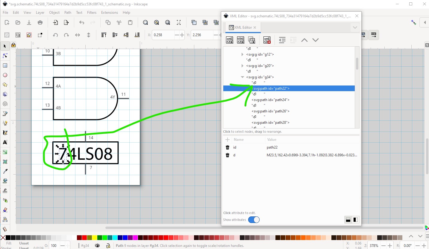
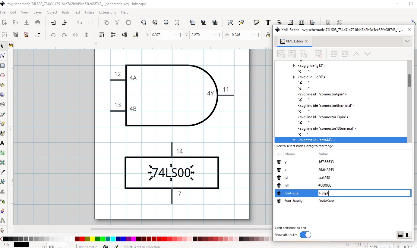
Looking at the 74ls08 schematic svg here is what I would do. Currently the text is paths, it is preferable that they be text (as then they are easier to change)
so delete all the paths to delete the text
then duplicate the 4A text above it, move it out of its current group and in to the subpart1 group, change the text from 4A to 74LS00 change the fill to #000000 (which is black) and increase the font size from 2.8 to 5 to make the text larger. There are actually specified sizes for text but I have ignored that here as it needs the svg scale to change for the normal values to work, I just made it somewhat larger. I would change all the other text font-sizes to be 5 as well so the text is larger. For the pin numbers the fill should be #555555, the label should be #000000. The sizes in px at the suggested 1/1000in per drawing unit values are listed in the graphics file format document here:
https://fritzing.org/fritzings-graphic-standards
actually they are specified in pts rather than px (which changes with scale) so I guess the standard values I use have been converted from points to px at the standard scale. Changing the font-size to 4.24pt like this
should set the correct size which equates to
5.66667px at the current scale. I also changed the pin numbers to be the correct size and color but only for the power subpart.
Here is a copy of the modified schematic svg (right click and save image as to download it)

Again, thank you so much.
I am interested in trying to fix it myself, even if I keep asking you for help ![]()
I commented out the paths and their headers (<g’s>), as you indicated
Copied and pasted straight after it the section for the number 4
</g>
<g transform=“matrix(1 0 0 1 17.5 170.4004)” >
<text fill=“#000000” font-family=“DroidSans” font-size=“11” >74LS00</text>
</g>
as you indicated, changing, the colour, font size and position. I now have the 74LS00 perfectly positioned in the box.
I will now alter the rest of the file to suit.
Again, thank you for your insight.
Bob.
Not a problem, that is how we learn.
What I usually do (as I have probably mentioned) is either ungroup the schematic group til there are no more groups (which as a bonus removes the transforms!) In the case of schematic subparts that also unfortunately removes the subpart groups which need to be added back in but it does make the svg much cleaner and easier to deal with.
Peter
I am trying to alter 74ls04 (an inverter) and save it as 74ls14 (a schmitt trigger inverter).
The only real difference is the small symbol in each gate of the schematic.
![]()
I have it as a jpg and an svg. The svg loaded into inkscape as a font letter (see the last paragraph) and the file is huge?
Is there any way I can add just the graphic above to the schematic file of the 74ls04 by adding a line something like I have done to add the small circle to the right side of each gate?
<ellipse stroke-miterlimit="10" stroke-width="0.6" cy="129.5"  cx="58.753" fill="none" stroke-linecap="round" rx="1.3" ry="1.3" stroke-linejoin="round"
 stroke="#010101"/> <!--this line makes the circle-->
If I could just add one and move it into position over each gate.
Before I sent this page I had a try at making the symbol into a text symbol.
I tried to set it in place over one of the gates
I have succeeded but for anyone else to see it they will of course have to have the font in their computer.
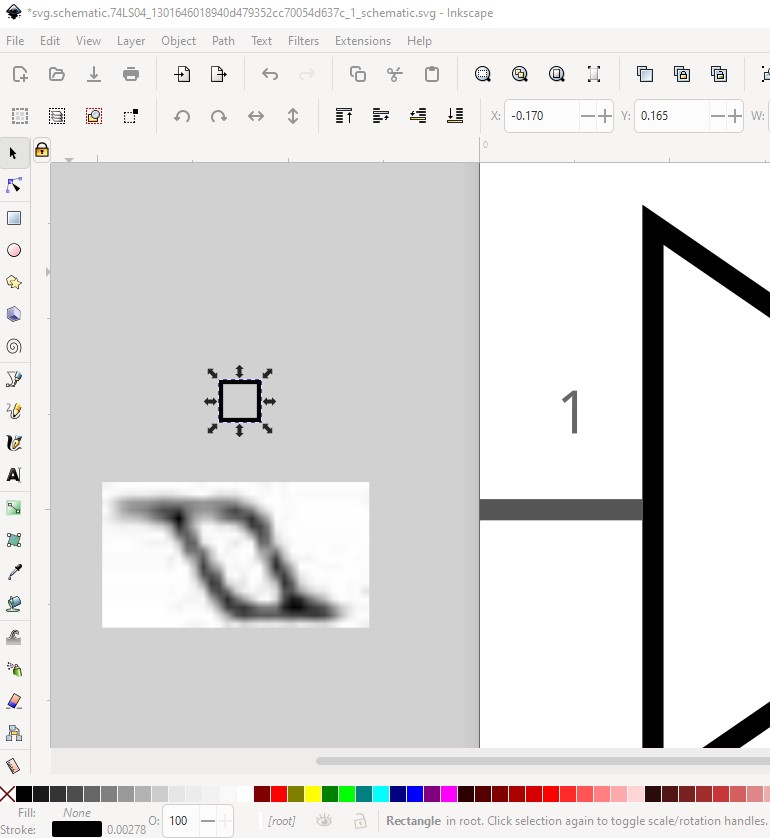
Yes, you need to create a new path like this
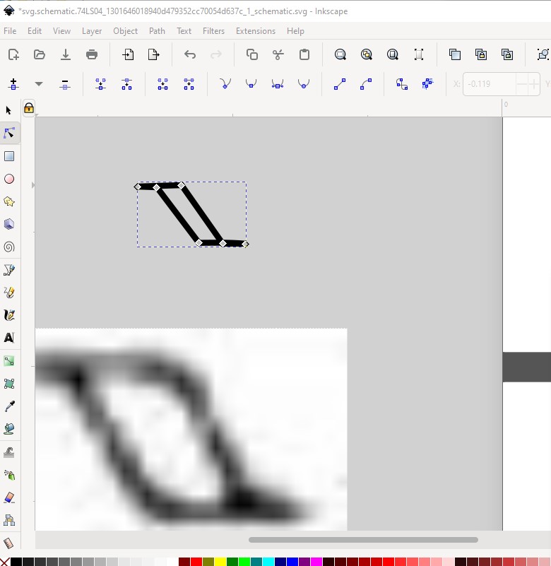
here I imported your jpg image and scaled it to approximately the right size then I convert it to a path by creating a rectangle of the correct size, selecting it and clicking Path->Object to path, then edit it with the path editor like this
then move the path in to the svg image like this
by moving it in to the correct subgroup and positioning it. From here you can adjust the size, scale and stroke width of the path to make it the correct size and appearance. Then duplicate that path and move it to the other subgroups. In general images translate poorly because they aren’t svg, you are usually better to recreate the image out of svg elements such as paths. Hope this helps. Here is the svg with the above path in it for reference

as usual right click and click save file as to download the svg. The change is in the first inverter element.
Peter
Hmm, I downloaded your svg file, replaced mine with it.
I can see the symbol.
I think I Altered the stroke width successfully but I cant see how to make it larger?
I copied the line to the same position in subpart2 but when I pull the ic onto the schematic I get a box that says file fails to load and then locks up?
I have to go into task manager to clear it.
If I have the line in the place you put it and then copy it to the same place below and then comment each one out the other works fine, (I have altered the position of the second one so it shows in the second box down).
If I change the path id of the second one to “rect394” (the first one is “rect373”) it still crashes?
What am I missing?
Easy enough:
Lock width to height (to keep the scale constant) set dim to mm to control size and set scale stroke-width when scaling to adjust the stroke width automatically (you can change it later if it gets too big) then click the width increment in the tool bar like this:
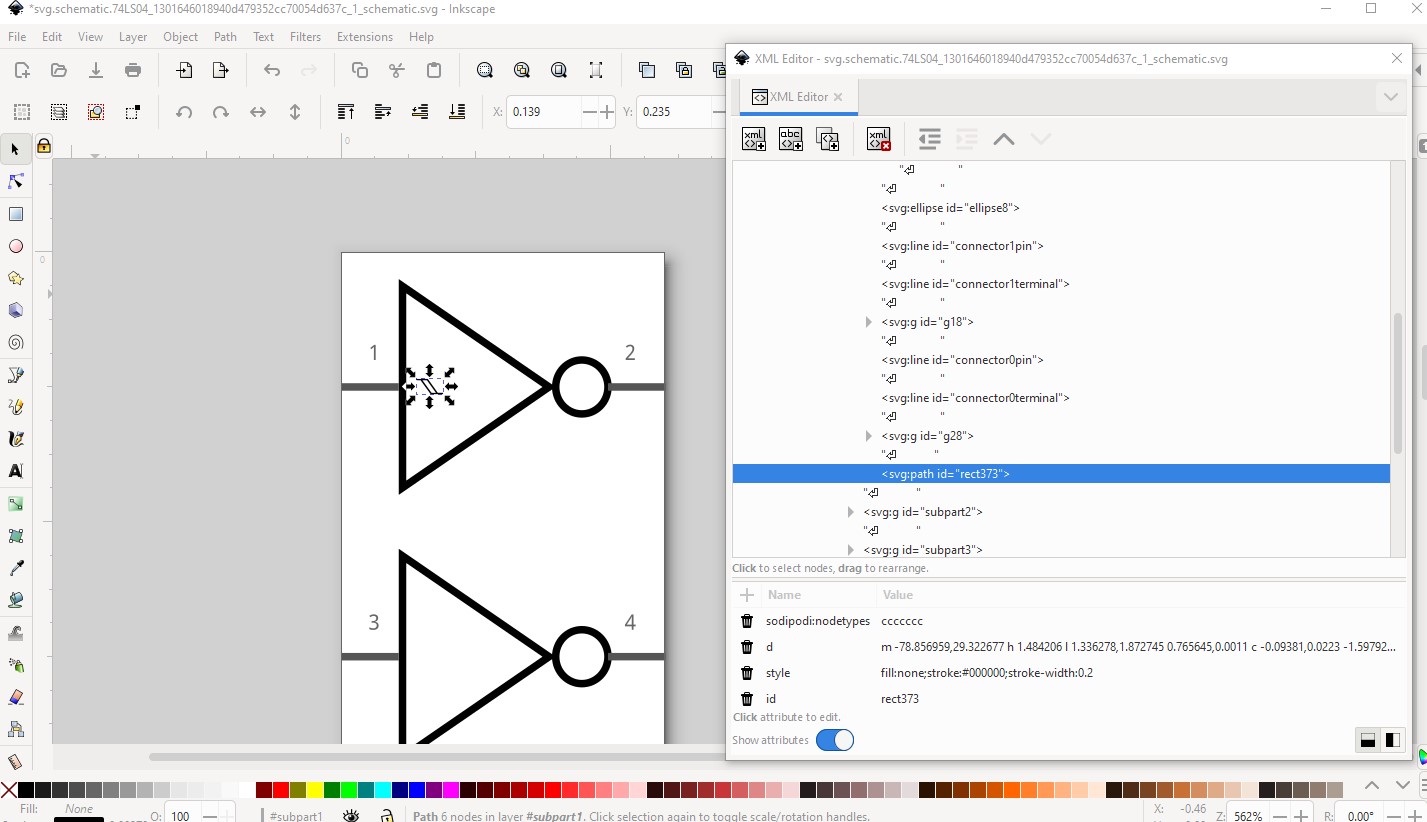
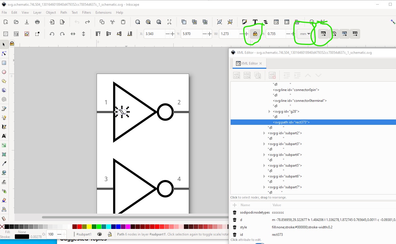
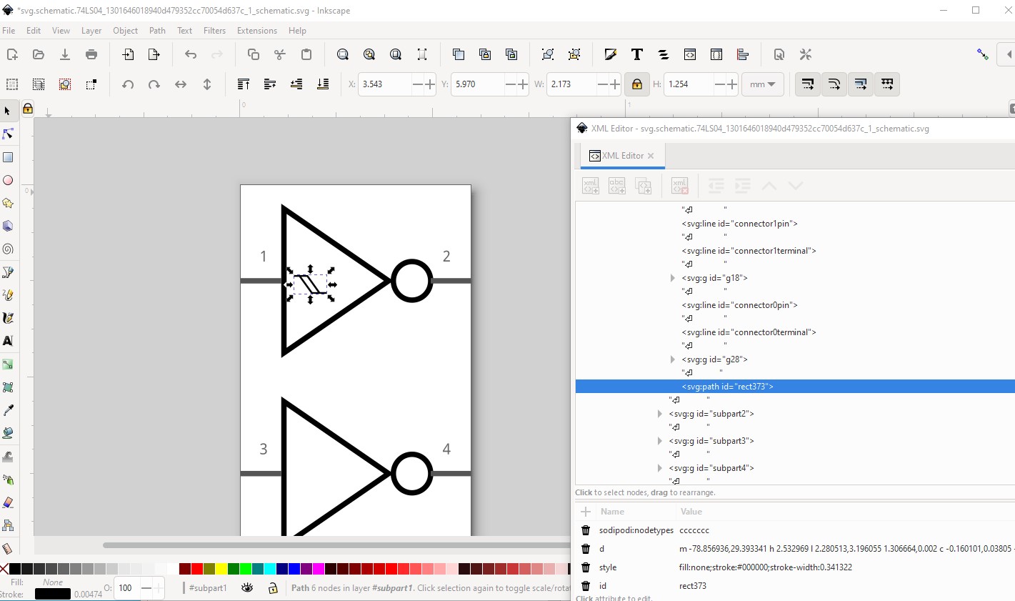
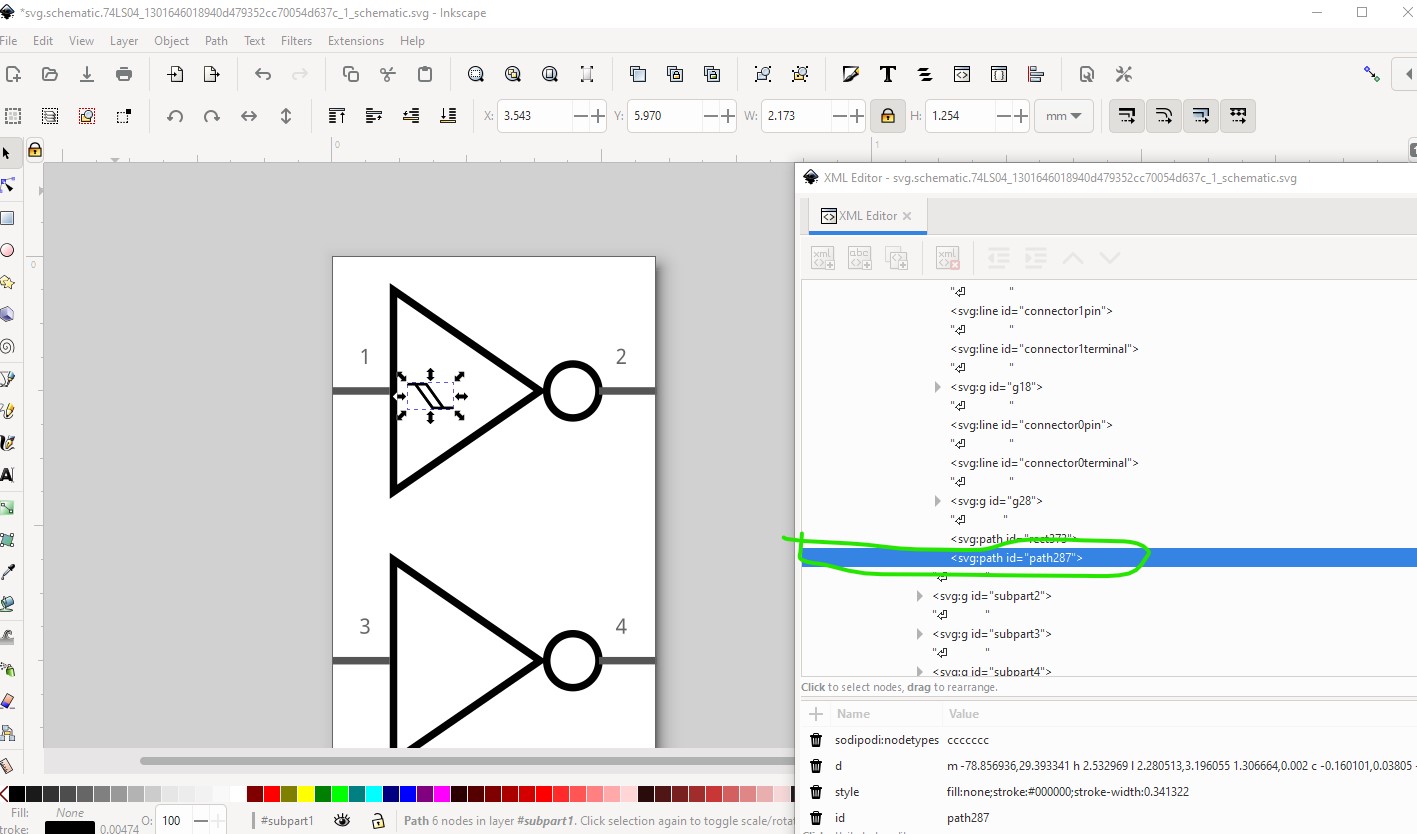
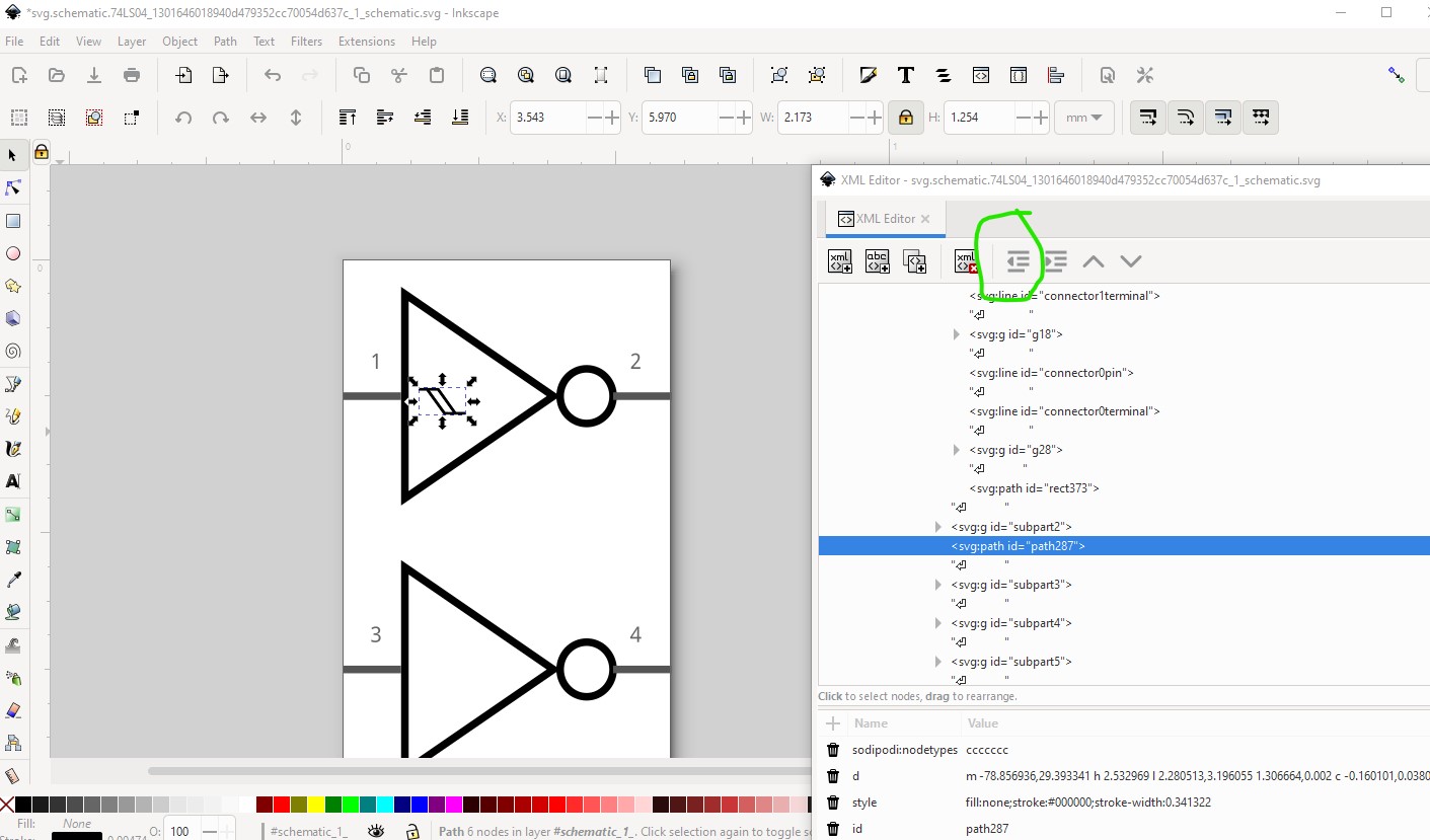
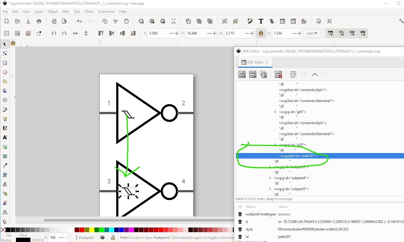
If you upload the svg that locks up I’ll have a look at it and can probably tell you what you are doing wrong. If you didn’t remove it from the subpart1 group that is likely what is wrong. Here I selected my modified path
then duplicated it to get a new one (still in subpart1)
now I need to move it out of the subpart1 group then move it below subgroup2 and indent it to get it in to subgroup2
then cloick and drag the path in the canvass to be in subpart2 like this
I expect (but haven’t made a part to try) that this will work. I suspect your new path is still part of subpart1 but is physically in subpart2 which will likely cause a problem such as you describe. Subparts are fairly complex to deal with …
Peter
I appreciate you sharing this useful information regarding IC chips that Bad Bunny can use.