Doit esp32 devkit v1

I want to share a part: It is a

DOIT ESP32 DEVKIT V1

with 30 pins. The pins are (obvious) in two rows and the distance between the two rows is 11pins (about 1000 mil). The pads are oblong/rectangular - so it is possible to route between pads.

I did a gerber export and let seedstudio produce testboards. The pads, the holes the routing between the pads look all ok. There might be issues with the breadboard view - I’m sorry for that, but I’m not using it. But schematic and PCB should be ok (at least as I found out so far).

(link removed - please follow the thread for the latest version)

1 Like

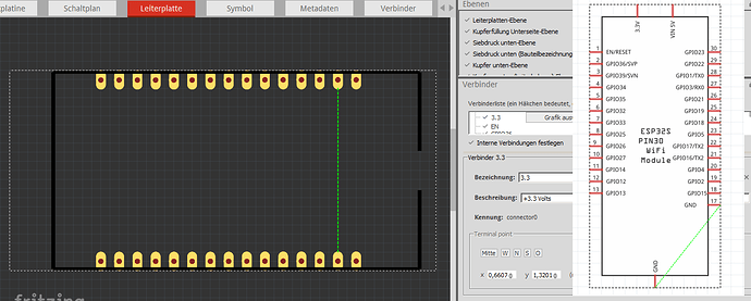
This appears to have a number of problems. As you noted breadboard isn’t complete (although the graphic part is very good so it would be worth it to correct it so the part works correctly for others). The connections on PCB appear totally wrong which may be a routing issue (or may not as schematic appears to be screwed up in the same way, pin one shows as pin 2 En / Reset) in schematic. If you load it in to Fritzing and hover over a pin in any view (pcb in this case) Fritzing will display the the pin number, Top right shows as pin 1 (as expected from the silkscreen outline) but it is listed as 3.3V not EN as the pin out diagram on google shows.The next pin left shows as pin 17 ground not pin 2 VP as it should (because the order of pins in the fzp file doesn’t match either schematic or pcb views). It is preferable for schematic to have the same layout as breadboard or pcb (i.e. 2 rows of 15 pins). A further look at pcb indicates pin1 in pcb is actually bottom left as for a standard IC (but not what the silkscreen outline is showing) and from there the pin numbers look correct (so just the hover over labels are wrong). I’d probably add the usb connectors to the silkscreen to make the alignment of the board obvious. All the pcb pins have pads (which aren’t used) as well and the fzp file has terminals defined in pcb (but not in the svg) which normally isn’t done. The gerber output indicates the pcb hole size is 0.032 which may get rounded up to the correct 0.038 for .1 headers by the board house, but it would be preferable to have that in the svg. There appears to be bus problems in the fzp file the ground pins don’t exist and the other 2 are not the grounds (2 random pins appear to be bused together). If you like I can fix this up to be a more standard part or you can do it to learn more about part making as you choose.

Edit: A closer look at this indicates more problems. You indicate the distance between rows is 1100 mill (i,e, 1.1 in which matches at least one other module like this I’ve dealt with, most of them are .9in) yet the gerber output shows the spacing to be 9979 mil (i.e about 1 inch not 1.1). Do you have boards that the module actually fits in to? I see the problem on breadboard is that the image is for one of the 18 pin per side units not a 15 pin as you have. I was trying to adjust that (there doesn’t appear to be any mechanical information about these boards on the web) when I came across this. I had assumed the pcb layout was correct and tried to adjust breadboard to match and it didn’t match. As well it would be desirable to put circles on the silkscreen in pcb view that the user can drag a hole over if they want the mounting holes to be drilled. That of course requires knowing the position of the mounting holes (which as noted I can’t find on line anywhere). If you could measure the positions with calipers on a real board that would help as would the height and width of the circuit board to check the silkscreen outline size which seems to small as it is overlapping the connectors.

Peter

Peter, thank you for crosschecking and your feedback.

You are absolutely right - it’s not 1100 mil. I messed it up: “11 pins width” are not more than 1000 mil. Any inaccuracy resulting in 997,9 in the Gerber comes from my nob-knowledge in Inkscape. However the pin-headers fit on my real PCB but as the presoldered pin-headers on my board are not soldered 100% perpendicular, this mismatch doesn’t have a big effect.

The hole/pad sizes come from the Sparkfun DIL 40 pin (as far as I remember). I did not change them in size. I just deleted one layer, deleted 10 pads/pins and renamed them. I had lot of problems to pick up the right graphics in PCB view for the connectors so it ended up, that the connectors are the rectangles and not the circles. I haven’t found any guideline that this is not allowed and it works (at least for me).

The connected pins are GND - therefore I decided to connected them internally (Pin 14 and Pin 17) in PCB view. In my opinion this should be ok.

Your indicated “It is preferable for schematic to have the same layout as breadboard” … there are a lot of modules where 5V/3.3V/VIN and GND are on the top/bottom of the schematic view. I liked that idea, therefore I did the same. I used the ESP32S-HiLetgo schematic SVG as starting point.

I don’t know why the “mouse over - in bracket numbering” doesn’t fit to anything else, but should I care? If I make a drawing in schematic view I connect connectors based on their naming (VIN, GPIO13…) and I do routing in PCB according to wiring, I never used the “in bracket numbering” for named parts where I have the pin names in clear text available.

The “overlapping” pads vs. silkscreen outline: I found the measurement of 28,3 x 51,5mm at the seller and started painting the PCB before the part arrived.

The “hole indicators” on the silkscreen are a good idea, i consider that for my next module (if I’ll ever make one). Currently I didn’t want holes as I needed a very small footprint part.

I can do a caliper measurement earliest during Christmas days.

P.S.: is there any up to date “Tutorial” / Guideline / Style-guide how to design parts? I just see a lot of “hints” in the forum but no actual description.
Ah, so the spacing should actually be 1 inch rather than 1.1?

yes 0.998 to 1.0 isn’t going to matter, 0.998 to 1.1 would be a bigger issue.

There aren’t many guidelines and “it works for me” is as good a criteria as any :-), I (and some other people) find a schematic that doesn’t match the bb / pcb views annoying (the Raspberry PIs are one such). Neither is right or wrong as both will work, it is just personal preference.

I’ll have to look again, but there are two buses, one with non existent pins (which won’t do anything) and the other I think connects two pins that are not ground, but I may have read it wrong.

That would be useful. as would height / width of the actual board (I couldn’t even find measurements on any of the sites selling that board that I found).

Unfortunately web site maintance along with development has pretty much died. Signup to the forums has been dead for months for instance, so we aren’t getting any new folks in here. I’m trying to get to the point of getting development at least possible, but it looks like interest in Fritzing has pretty much died. I’ll fix up your part a bit (make breadboard work, fix up the buses etc) and post what I would do to make this part. I’ll guess at the position of the mounting holes til we get measurements.

Peter

1 Like

Keep at it

yes the part is just 1 inch only.

sorry, I only find that one internal bus in pcb and schematic view, where do you see two of them?

in the fzp file for the part (which defines the buses) there is a second bus but with non existent pins (the parts checker flagged it). It is likely a leftover from what ever part you cloned. The two ground pins are indeed bused correctly, clicking on one of the grounds lights both it and the other ground pin yellow as it should. The fzp file labels are therefore wrong as they indicate non ground pins (that will be why the labels come up wrong when you hover over them as well).

Peter

OK here is an improved (but likely not a direct replacement) version of your part. Much of the change isn’t visible directly. Breadboard has been fully implemented so it now works correctly (that is probably the most visible change). All the svgs have been rescaled to standard scale, Schematic has been made smaller and to match the bb and pcb views. Pcb has a bunch of unneeded elements removed and the pads with holes set to 0.038in (suitable for .1 headers) and aligned to .1in pitch and 1.0 in width. Pin numbers now start at 0 with pin 1 (connector0 internally) the bottom right pin. The labels have been corrected so that hovering over a pin will give you the label that appears on the PCB for that pin, the pin number (1 to 30, which also now appears on the pcb silkscreen) and your description of alternate uses. Remaining to be done are mounting holes on the pcb silkscreen (and on BB where they are present but probably not in the correct position) and the board outline which need measurements from a real board. This was created as a new part so it will load alongside your original for comparison.

Edit: replace the last version with a more accurate one (although possibly not the final version yet). The board size and mounting holes should be close to correct in this one, but need to be verified against the actual board yet (as I don’t have one).

Edit2: In pcb, remove the pin numbers and replace them with the 3V3 designation from the pcb on pin 1, so it matches the labeling on the board. Replace the solid pads for the mounting holes with rings to make it more obvious that they are mounting holes (although not drilled by default).

edit Mar 2024

correct a typo on GPIO16 (is TX2 should be RX2)

DOIT Esp32 DevKit v1 improved.fzpz (34.8 KB)

Peter

4 Likes

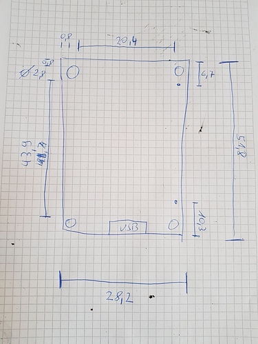
Peter, here are my measurements:
the board is 28.2 x 51.8 mm
the holesize is 2.8mm, the padding to the boarder is 0.8 and 0.8 mm
the distance between top and bottom of the holes is 43.9
the pins on the top start at ca 6.7mm
the pins on the end start at ca 10.3mm

if you need more information, please let me know.

Good job! I’ve updated both breadboard and PCB views to reflect the new measurements (which are internally consistent which is a good sign :slight_smile: ), if you could print the PCB svg at life size and compare the output to the real board to make sure the mounting holes and the header connectors in the pcb view match an actual board we should have a part that is ready to be submitted to core. I replaced the board one post back with the updated one so we don’t have multiple copies of the same board floating around. If it isn’t quite right, you can move the mounting holes and/or connectors in Inkscape (you probably have to ungroup the pcb svg to avoid translates though) until they match exactly, then I’ll update the pcb svg to match if needed.

Peter

Peter, I checked the updated version and the pcb printout looks ok when I compare it to the real part. There are two things I would like to bring up:
a) the “false fixing holes” should not be filled to make it very clear that these are not holes which get drilled but only marks printed on the silkscreen. Please use empty circles instead, I recommend even a dotted line.
b) please delete the pin-numbering 1/15/16/30 on the silkscreen. There is no fitting numbering on the board, and I see no need to number pins on the PCB in that way. I have 3 different boards with the same pin out from different sellers, none of them are numbered 1-30. So I recommend that you leave away that 1/15/16/30 on the silkscreen also. You might mark pin 1 with a dot, like it is done with some IC, but for me the symbolic USB socket and the asymmetrical pin-distance is enough to get the module right on the board. If you still insist on a labeling, please use pin 16 labeled as EN (enable/reset), as this is - at least for me - the most significant pin at the beginning of one side and one pin is clear enough to do the right alignment of the module

Good suggestions, implemented and the board replaced again!

Peter

Peter, looks very nice now. I will export some Gerber files now and send them to fab. Thank you for your assistance.

Happy to help. The boards are the acid test for how well we did :slight_smile: they will tell us for sure if the mounting hole alignment is right when the headers are inserted in the board the mounting holes on the silk (or the real holes which ever you use) should match up (and we can move them if not).

Peter

is there a improved-improved version of [DOIT Esp32 DevKit v1 improved.fzpz]?

No. so far what you see is what you get. Improved in what way?

Peter

I took this one. Shape is good but only one pin is described (3v3).

Get 0.93b no parts updates anymore?
I notie there are many variants of the esp32 … too many …

The pins are all described in schematic and if you hover over a pin in any view in the DOIT Esp32 DevKit v1 improved.fzpz file above (and I expect in the original as well , because I am unlikely to have done it.) If you post a screen shot of what you think is missing I will look further. Parts update works fine, no one much (including me) is submitting parts to github which is currently the only way they get added to core (for that matter not a lot of people are making parts at all any more …) If you are running Win7 and 0.9.3b parts update is broken and you need to upgrade to 0.9.4 to get it working again. In my case I haven’t figured out how to keep the three repos in sync so don’t even try any more. There are a lot of variants of the esp32 because there are a lot of slightly different versions (I have made or modified more than half a dozen of them.) If you own an odd board you want a part for it and by and large we have obliged. I haven’t seen a new request in a couple of years I don’t think. This was likely the last one and it is 2 years old now.

Peter