How did you create you copper logo? I create exposed copper artwork on my pcbs all the time and to do it I start with a test point and change the SVG to image I want. The function in Fritzing for copper artwork just makes it in the copper but under the solder resist. My best guess as to why Aisler is not rendering yours as either exposed or covered copper is likely to be related to your SVG having open paths which can result in the infill leaking and filling the entire image area. It could also be that your SVG has other issues but either way I would say it is your SVG. I am attaching an SVG I know works here for you to test. Just replace your image with this one and see if Aisler renders it correctly.
I actually used adobe illustrator to create the logo, all from scratch. I just modified the source of the copper image. I have tested your svg image and it renders perfectly in the lab’s preview:
I actually had some open paths in my svg image but I closed them, so maybe it’s another problem with my file. Do you know if there’s any tool to check for possible issues of my logo?
No but if you upload the SVG by itself I will have a look at it (I can’t extract it from the sketch).
You should note that Fritzing SVGs have to comply to SVG Tiny1.2 standards so it may be possible your SVG has elements in it that Fritzings does not like. It may also be that some of your paths need to be simplified or they are objects that need to be converted to paths.
I wasn’t actually saving it in Tiny1.2 - but I tried now to save it that way and it was complaining about the transparency (and that it was not able to save it).
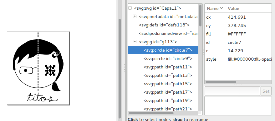
I will definitively use your fixing solution in the future! One last thing, why does the eyes appear white? Is it because the system detects them as a pinhole?
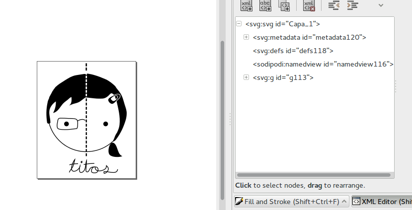
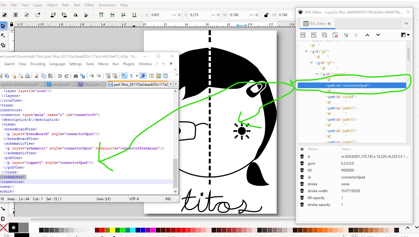
It sees any circles as holes. You need to convert the circle to a path. In Inkscape you select the circle and go to path/object to path and that changes it to a path from a circle.
You can see the xml data changes when you do object to path.
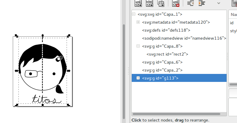
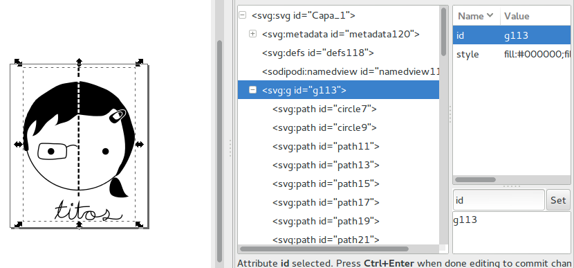
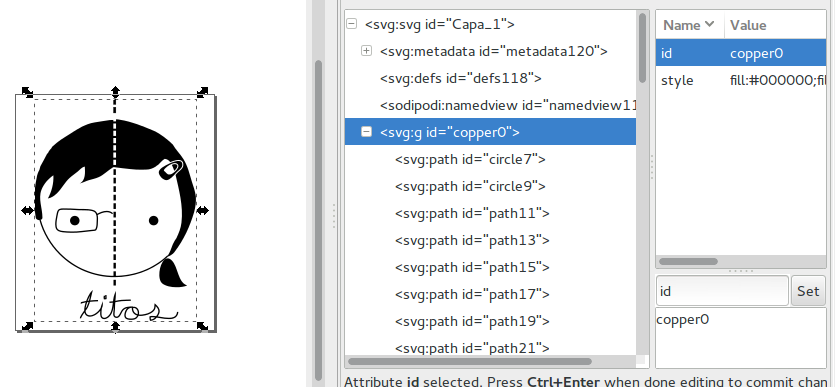
I took your picture and changed the id of the group from g113 to copper1 for the bottom layer or copper0 for the top layer. Or you can put copper1 inside of a group called copper 0 and it will work for both layers.
I then resized your image to 12.7mm wide as that was the size of the picture on the pcb and saved it as a plain svg.
After that I opened one of my existing bare copper parts based on a test point in the Fritzing parts editor and changed the images to this new image and assigned the right eye as the connection point (you have to hold down shift and scroll over the eye after clicking assign pin to choice the eye which is below the other parts of the image). Then it was just changing the meta data and saving as a new part. I then export the part for you. If you want to make other ones just change the svg in the parts editor.
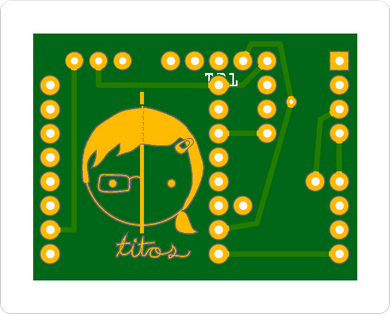
Then you place the part on your sketch (you may need to disable align to grid in the view menu to get it where you want it). If you have the pcb made by Aisler you will get gold a gold plated image.
Edit the image appears to be reversed. I will update this post when I figure out why.
@segfault
EDIT 2: I figured out why it was reversed. copper0 is the top layer and copper1 in the bottom layer and if copper1 is inside copper0 it is universal. I have updated the instructions to reflect this.
EDIT 3: Here is the updated part that works for both sides. Titos.fzpz (41.1 KB)
Hi, I have exactly the same issue. I try to get the logo attached in bare copper, but is keeps on showing it with the solder mask on top. Can you please tell me what to do?
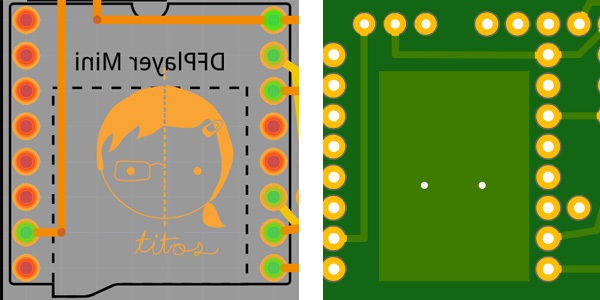
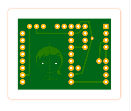
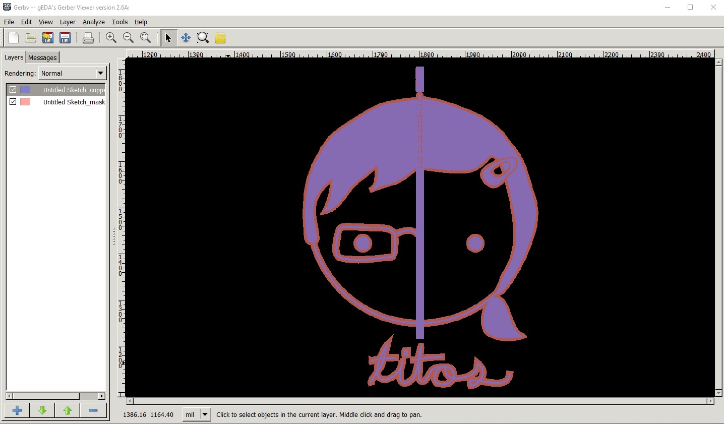
I don’t know if @sublimeartistry is still reading the forums he hasn’t posted in a number of years. In any case your problems sounds like you haven’t defined a connector for the copper. That is what Fritzing uses to decide if the copper is masked or not. From the original part it appears to me there is more copper umasked than I expect as it should be only the circle that defines the connector, the unconnected copper should still be masked. As well we would need to know if you want the image on both sides of the board or only the top or bottom (which is more complex to arrange.) This is the pcb svg from Titos.fzpz above:
the copper is unmasked because the circle selected is defined as a connector in both the svg and the fzp file so Fritzing knows it is a connector and will unmask any copper connected to it. Like this
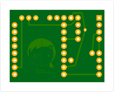
This is the copper1 layer (purple) and the top mask layer (orange) displayed in the gerbv gerber viewer. It appears to have unmasked all the copper (although as noted I wouldn’t expect that as most of the copper is unconnected to the pad) which may do what you want. The best bet is likely to upload the sketch (the .fzz file, upload is 7th icon from the left in the reply menu) which will give me the entire sketch to work on.
Hi Peter, Thank you for your swift reply on this post. I have done quite some designing with Fritzing, but designing parts never worked out so far. What I see online is that all tutorials are based on older versions of Fritzing… Is there any video or other tutorial guiding you trough the SVG designing process and generating new parts? I managed to design a PCB, but drawing parts is really complicated as far as I can see now…
These two tutorials cover current versions of Fritzing:
I lately learned there aren’t links to the videos in Old_Grey’s tutorial so you need to do a google search for the title and then they come up on YouTube.
Parts making is a complex process, and what you are trying to do is odd even for that. What are you trying to do with the logo? Obviously you want bare copper (no mask) but do you want that for only the copper of the logo (which the current process will do, although it may need super thin 8thou traces added to connect all the copper to the connection to achieve) or a rectangle around the logo with no mask on either the board or the copper (that is possible with the invisible copper trick)? I can easily enough make your logo in to a part for you using the current example (which has the logo only on the top layer) or an invisible copper implementation where the “copper” has a fill of none so no copper will appear but it will block the mask (usually used for touch pads.)