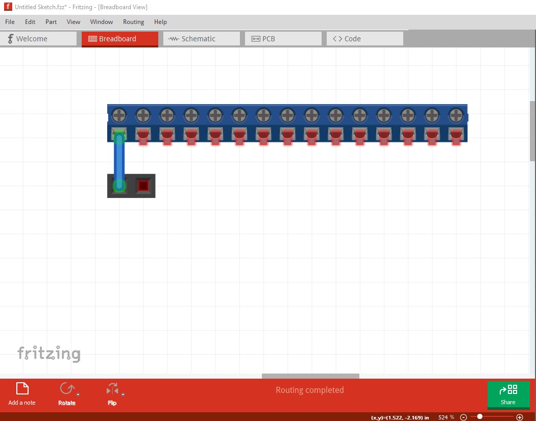
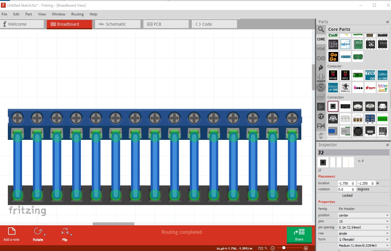
Breadboard looks fine as is
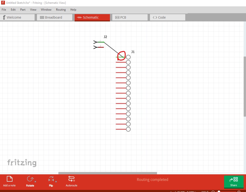
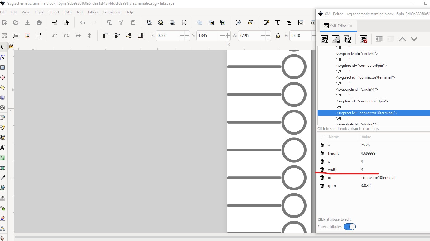
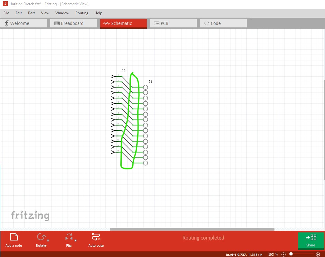
schematic is missing terminalIds and thus the wire connects in the middle of the pin rather than the end:
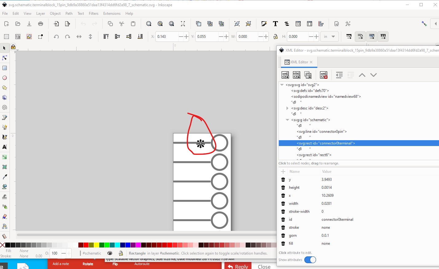
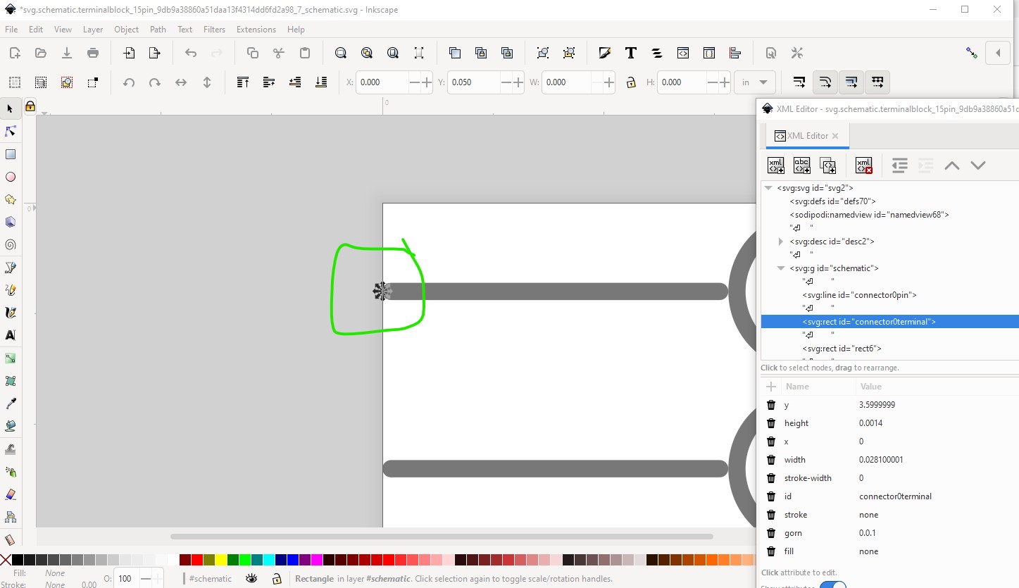
the terminalId is present, just in the wrong place in the svg:
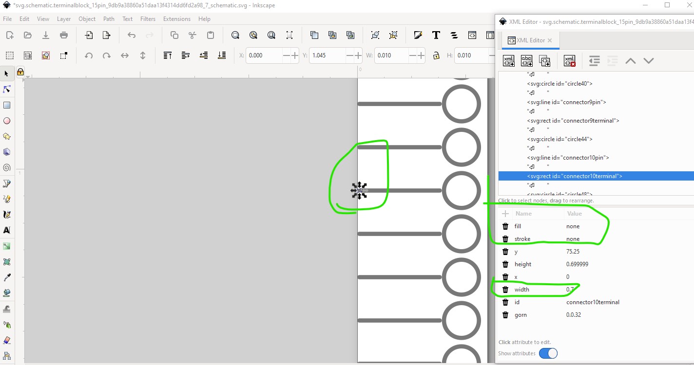
Change them like this and it will work.
on the ones other than the first one it was necessary to add a stroke and fill attribute of none and set the width to be 0.7 to match the height like this (in Inkscape, don’t know about Illustrator!)
to
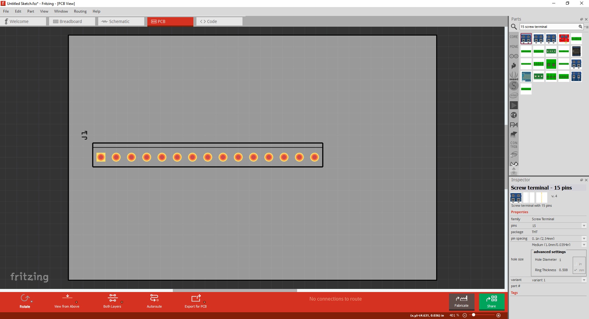
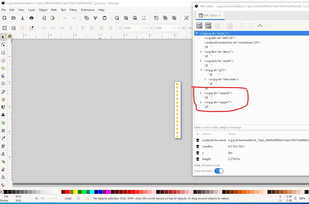
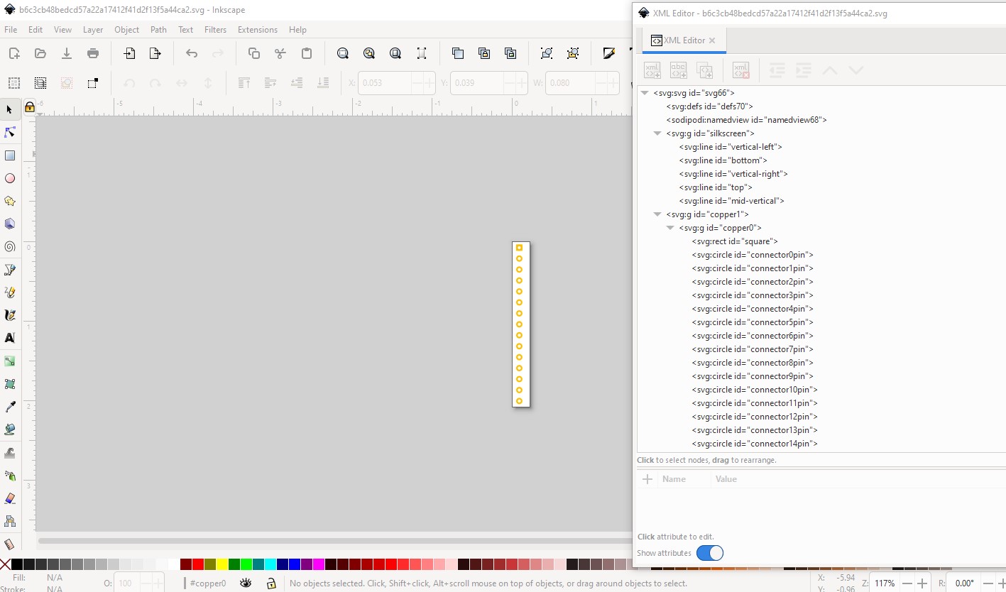
Pcb is incorrectly configured which is why the red rectangle.
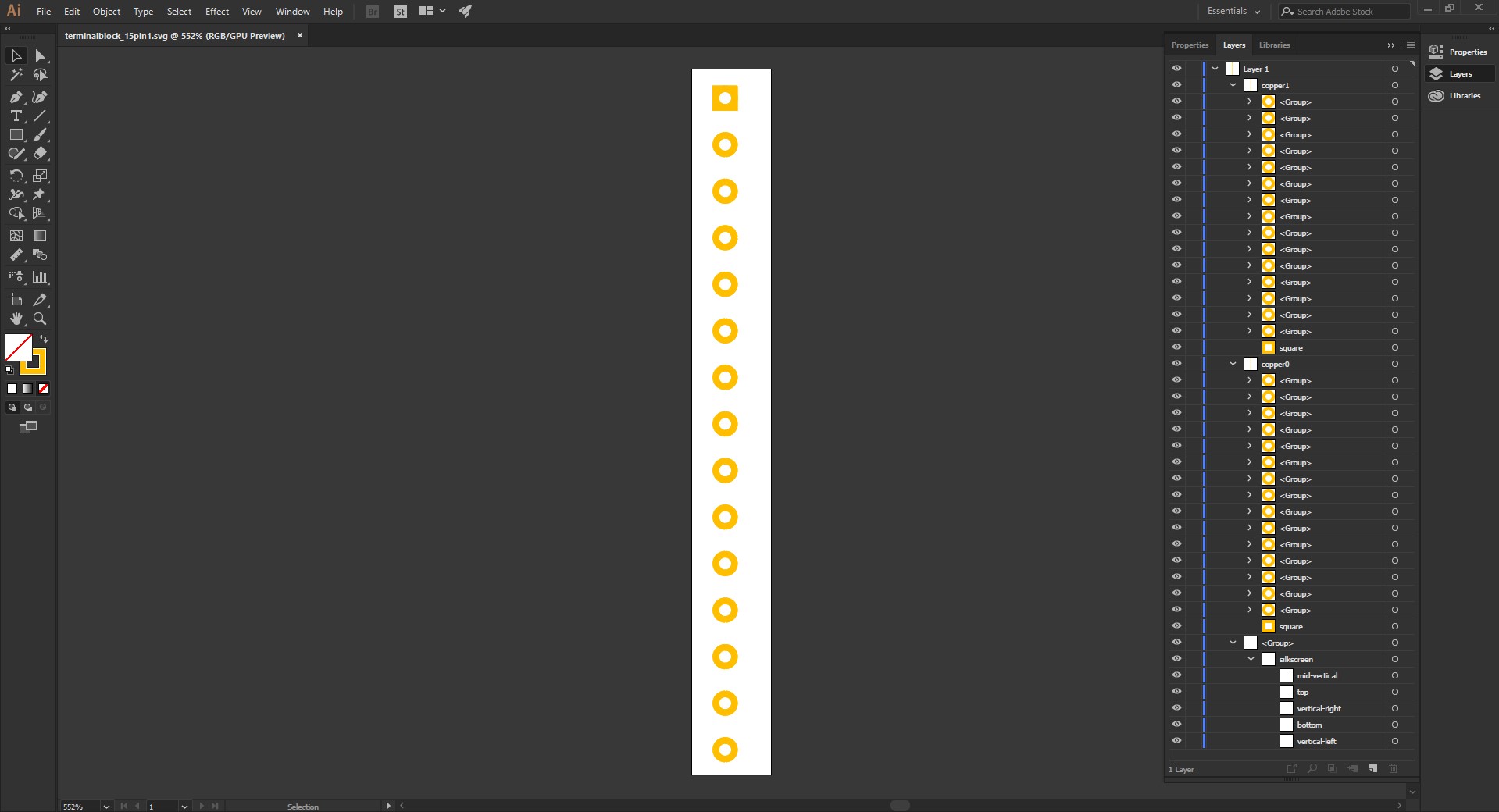
it needs to look like Blues’s svg with copper0 being a subgroup of copper1
I will just replace your pcb svg with Blue’s (rather than spending time to fix yours) and that should fix things. Running the resulting part through FritzingCheckPart.py (detailed in my tutorial) indicates a problem with Blue’s pcb svg. The svg is dimensioned in px which can cause scaling problems in Fritzing. Your svg above is dimensioned in in which makes it dimensionally correct and may be the source of Blue’s different pitch. It is worth printing out the pcb footprint at 1:1 scale and comparing it to a real part before ordering boards though.
Warning 19: File
‘svg.pcb.terminalblock_15pin_9db9a38860a51daa13f4314dd6fd2a98_7_pcb.svg.bak’
At line 3
Height 151.699px is defined in px
in or mm is a better option (px can cause scaling problems!)
Warning 19: File
‘svg.pcb.terminalblock_15pin_9db9a38860a51daa13f4314dd6fd2a98_7_pcb.svg.bak’
At line 3
Width 18.432px is defined in px
in or mm is a better option (px can cause scaling problems!)
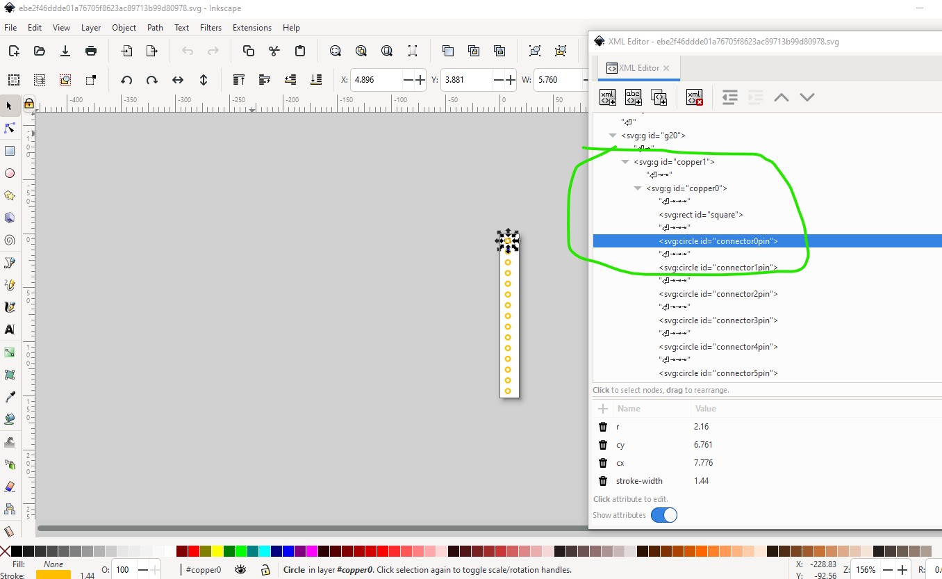
This actually appears to be an issue that Blue introduced as your original svg is correctly dimensioned in inches, so I will start from it and make the changes there. The corrected svg looks like this
with a silkscreen group (which you had) and nested copper1 and copper0 groups and hopefully the correct pitch. That produces this working part
terminalblock_15pin1-fixed.fzpz (8.9 KB)
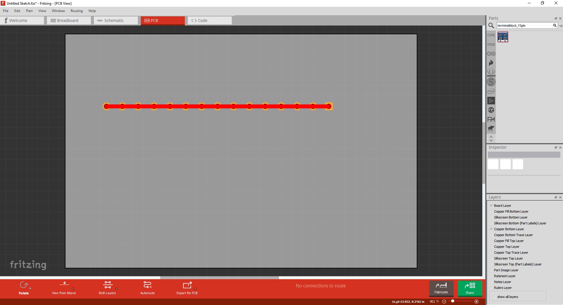
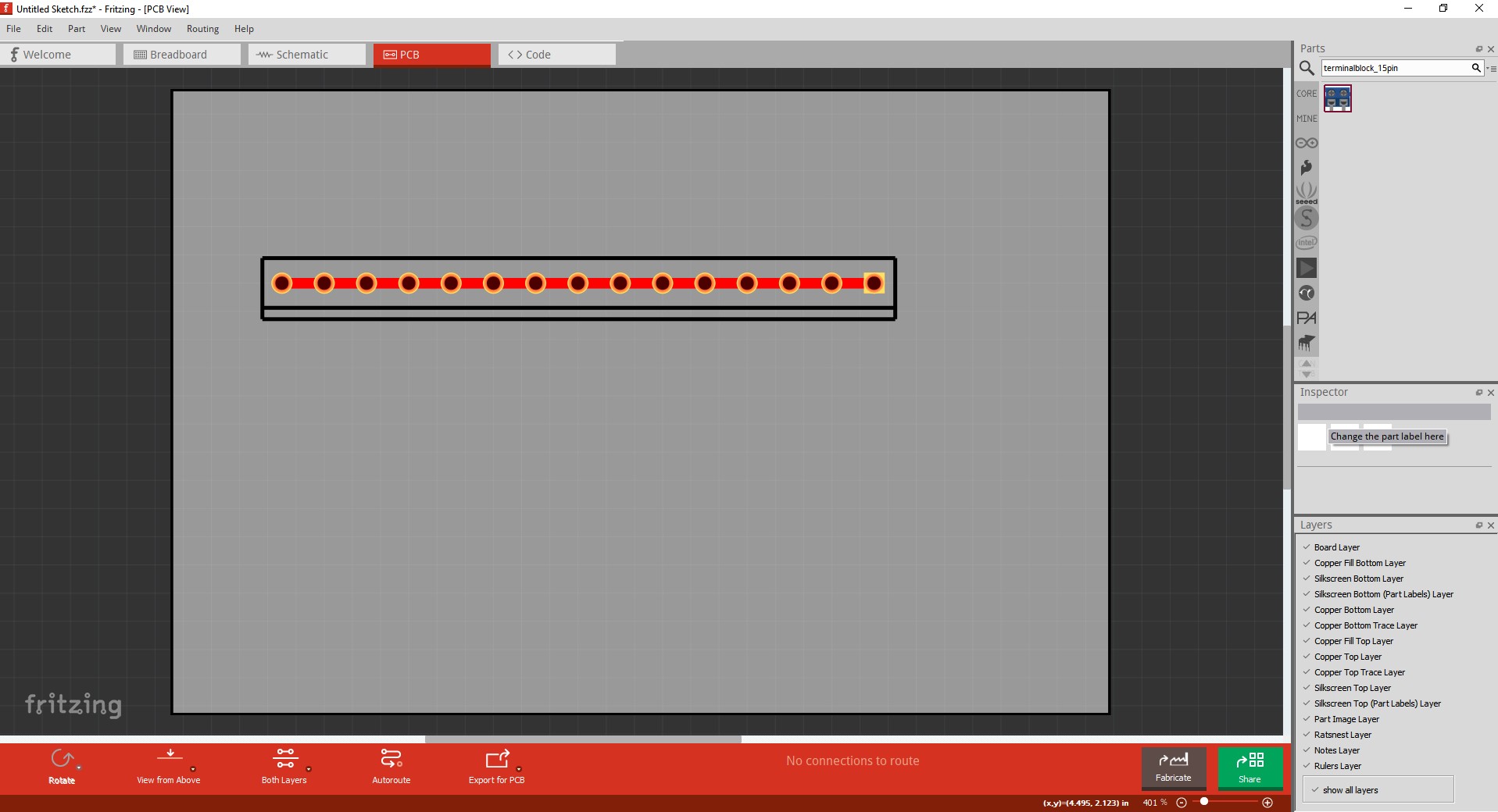
In turn this part looks like this in Fritzing
(I didn’t change the moduleId or file names so you will need to delete your current part in Fritzing to load this one!)
As we see pcb now works correctly. Whether it is correct or not depends on your original breadboard svg. One thing that may be incorrect is the hole size of the pads. They are currently set to 0.04in (found by exporting the sketch to gerber files and looking in the drill.txt output file.) That may or may not fit the terminals you are using and should be checked before ordering boards. Hope this helps, and if you have questions feel free to ask!
Peter