You may want to repost this to a new topic in the parts submit catagory as here it will show up as an unread item but not appear on the new posts items and thus won’t be seen by 99% of the folks.
edit:
As well there are a number of errors. The .fzp file needs a fritzing version, as of 1.0.5 the lack causes an error message like this
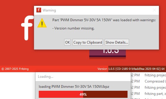
on 1.0.4 it will just load, but on 1.0.5 you need to click OK to acknowledge the message before it will load. To fix it in the .fzp file this
<module moduleId="Dimmer_71fd44826a2ca4b38ae98fcacef9ec42_6" referenceFile="generic_sip_4_300mil.fzp">
needs to change to this
<module moduleId="Dimmer_71fd44826a2ca4b38ae98fcacef9ec42_6" referenceFile="generic_sip_4_300mil.fzp" fritzingVersion="1.0.4">
which will clear it and allow the part to load without complaint. More serious is the pcb svg is not configured correctly and the pins are ellipses not circles. FritzingCheckPart.py flags the following errors
Error 69: File
‘svg.pcb.Dimmer_41c0fb5045b6861470d6a5a53c67536c_2_pcb.svg.bak’
At line 15
Found a drawing element before a layerId (or no layerId)
Error 65: File
‘svg.pcb.Dimmer_41c0fb5045b6861470d6a5a53c67536c_2_pcb.svg.bak’
At line 25
Connector connector0pin is an ellipse not a circle, (gerber generation will break.)
Error 74: File
‘svg.pcb.Dimmer_41c0fb5045b6861470d6a5a53c67536c_2_pcb.svg.bak’
At line 25
Connector connector0pin has no radius no hole will be generated
Error 65: File
‘svg.pcb.Dimmer_41c0fb5045b6861470d6a5a53c67536c_2_pcb.svg.bak’
At line 26
Connector connector1pin is an ellipse not a circle, (gerber generation will break.)
Error 74: File
‘svg.pcb.Dimmer_41c0fb5045b6861470d6a5a53c67536c_2_pcb.svg.bak’
At line 26
Connector connector1pin has no radius no hole will be generated
Error 65: File
‘svg.pcb.Dimmer_41c0fb5045b6861470d6a5a53c67536c_2_pcb.svg.bak’
At line 27
Connector connector2pin is an ellipse not a circle, (gerber generation will break.)
Error 74: File
‘svg.pcb.Dimmer_41c0fb5045b6861470d6a5a53c67536c_2_pcb.svg.bak’
At line 27
Connector connector2pin has no radius no hole will be generated
Error 65: File
‘svg.pcb.Dimmer_41c0fb5045b6861470d6a5a53c67536c_2_pcb.svg.bak’
At line 28
Connector connector3pin is an ellipse not a circle, (gerber generation will break.)
Error 74: File
‘svg.pcb.Dimmer_41c0fb5045b6861470d6a5a53c67536c_2_pcb.svg.bak’
At line 28
Connector connector3pin has no radius no hole will be generated
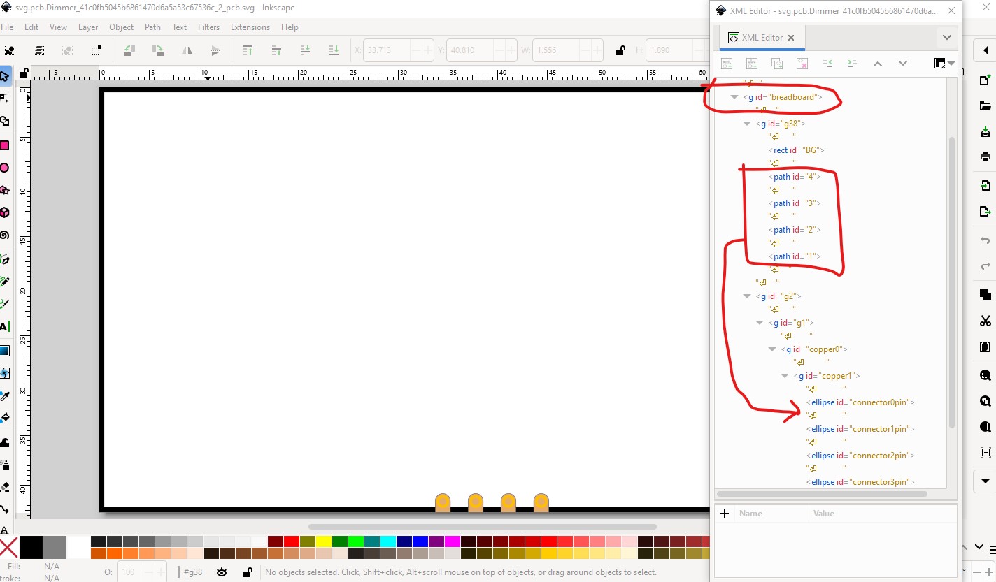
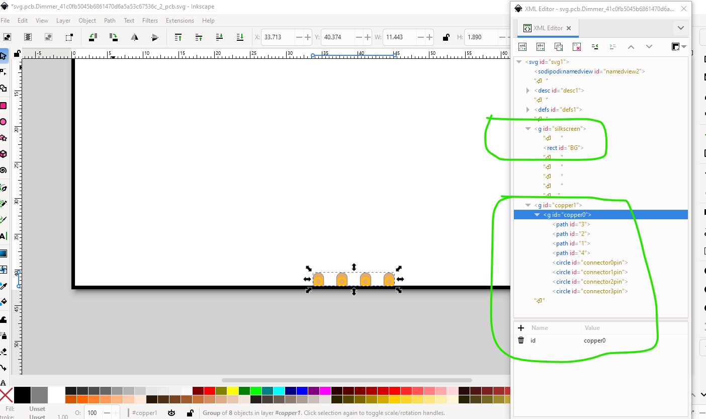
The layerId error is that breadboard group needs to change to silkscreen (which unlike breadboard is a valid pcb layerId) and the 4 paths need to move in to the copper group like this
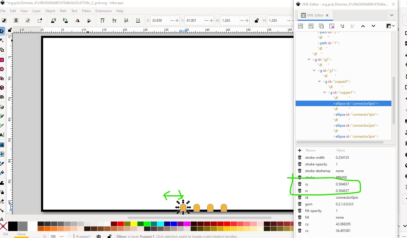
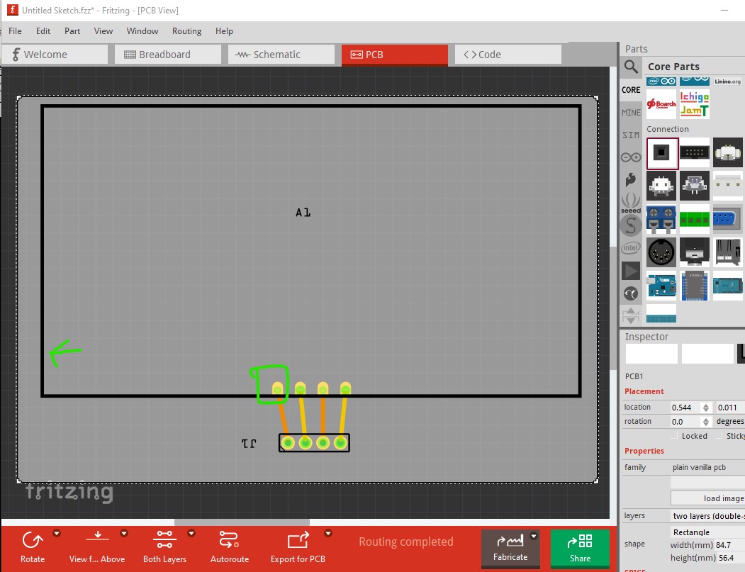
so they will be rendered as copper. The pads need to be circles not ellipses as they currently are
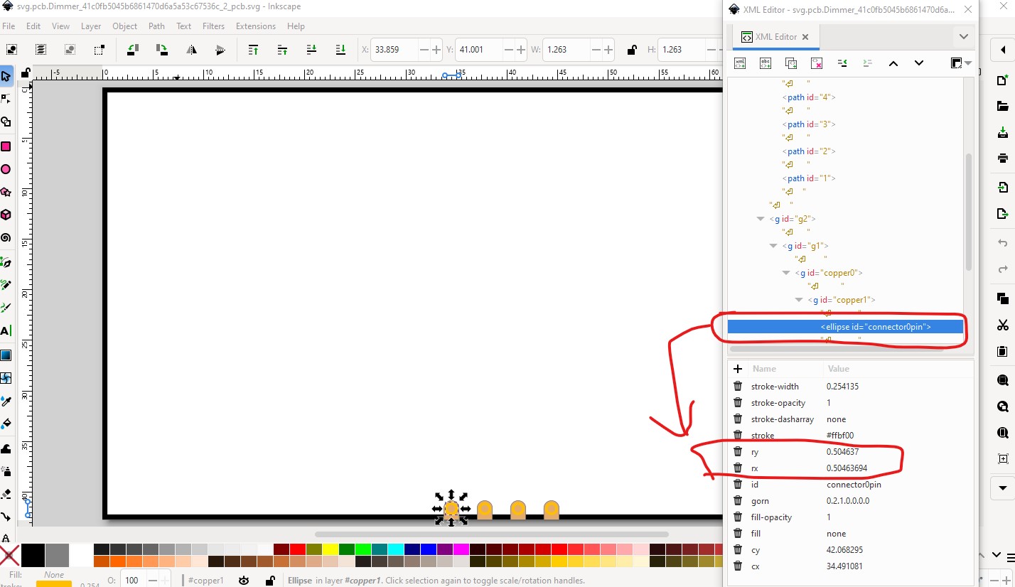
the easiest way to fix that is set rx and ry to the same value then move the pad 1 position in x or y and then back to the original position in the direction of the green arrow in this image.
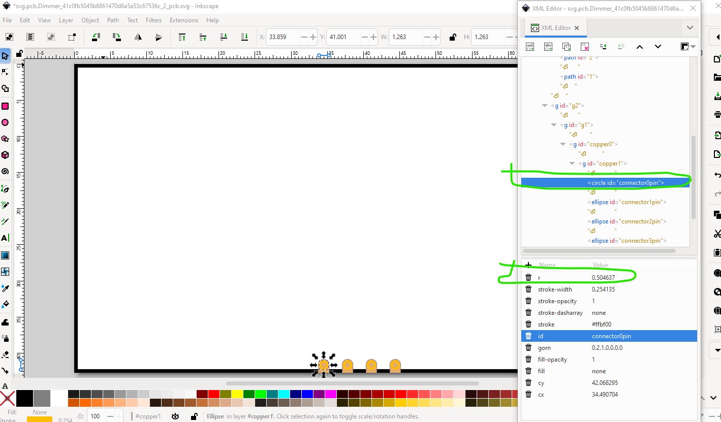
that changes the ellipse to a circle and creates a radius (r rather than rx and ry which gerber processing won’t process) like this
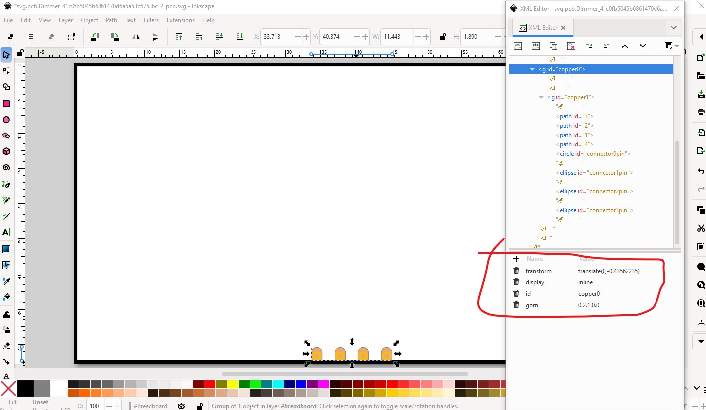
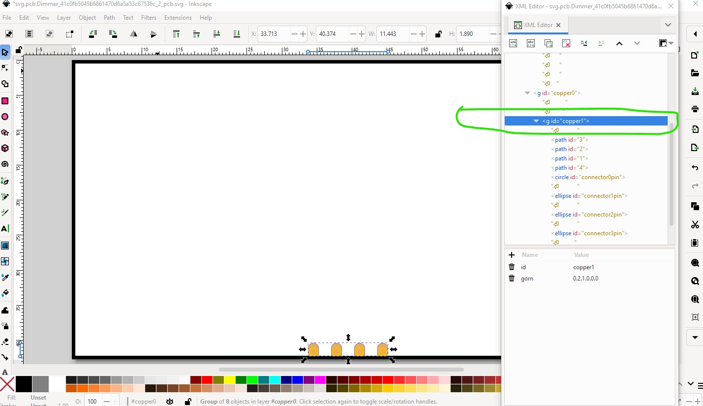
do the same for the other 3 pads and you should be good to go (as long as the hole sizes are set to a suitable value.) Just noticed an additional problem (that FritzingCheckPart likely flagged but I didn’t see) there is a transform in one copper group that isn’t in the other which will cause an offset in gerber processing (or at least used to.) The fix is to ungroup the copper groups and then regroup them without transforms.
The end result is this svg with all pads circles and no transforms in either copper layer.
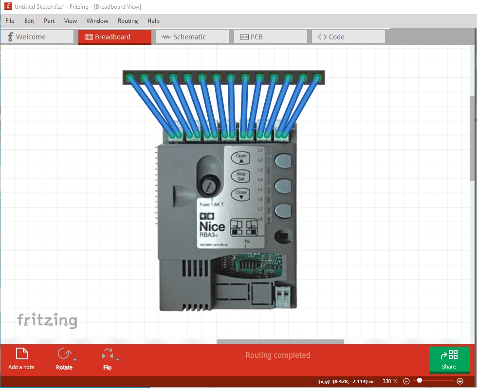
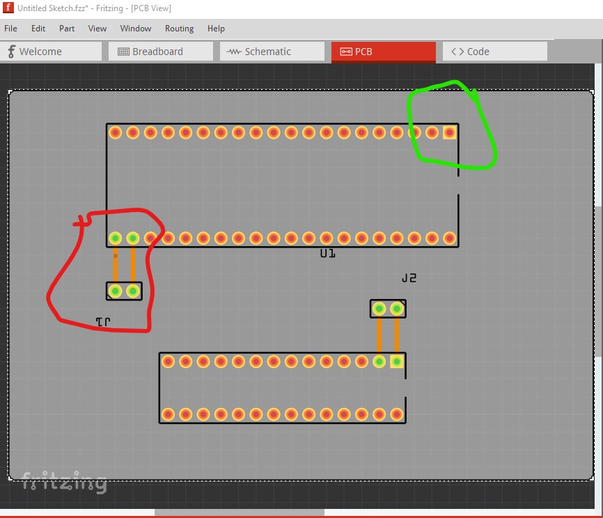
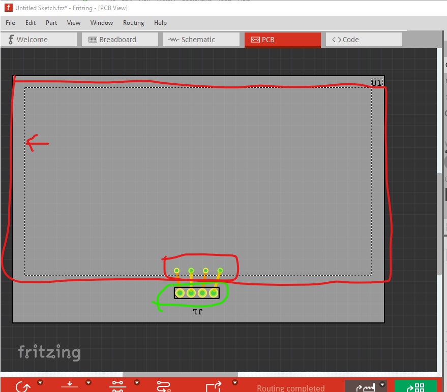
This is your original part with a 4 pin header connected in pcb view
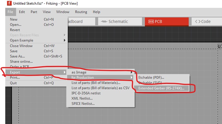
note the lack of a silkscreen layerId has caused the rectangle to not be rendered (it also won’t appear on silkscreen in the gerbers as we will see.) As well it is very likely the holes in the pads are too small. The headers are 0.038in your holes are much smaller (how much smaller we will see in the gerber files.) So now export the sketch as gerbers like this
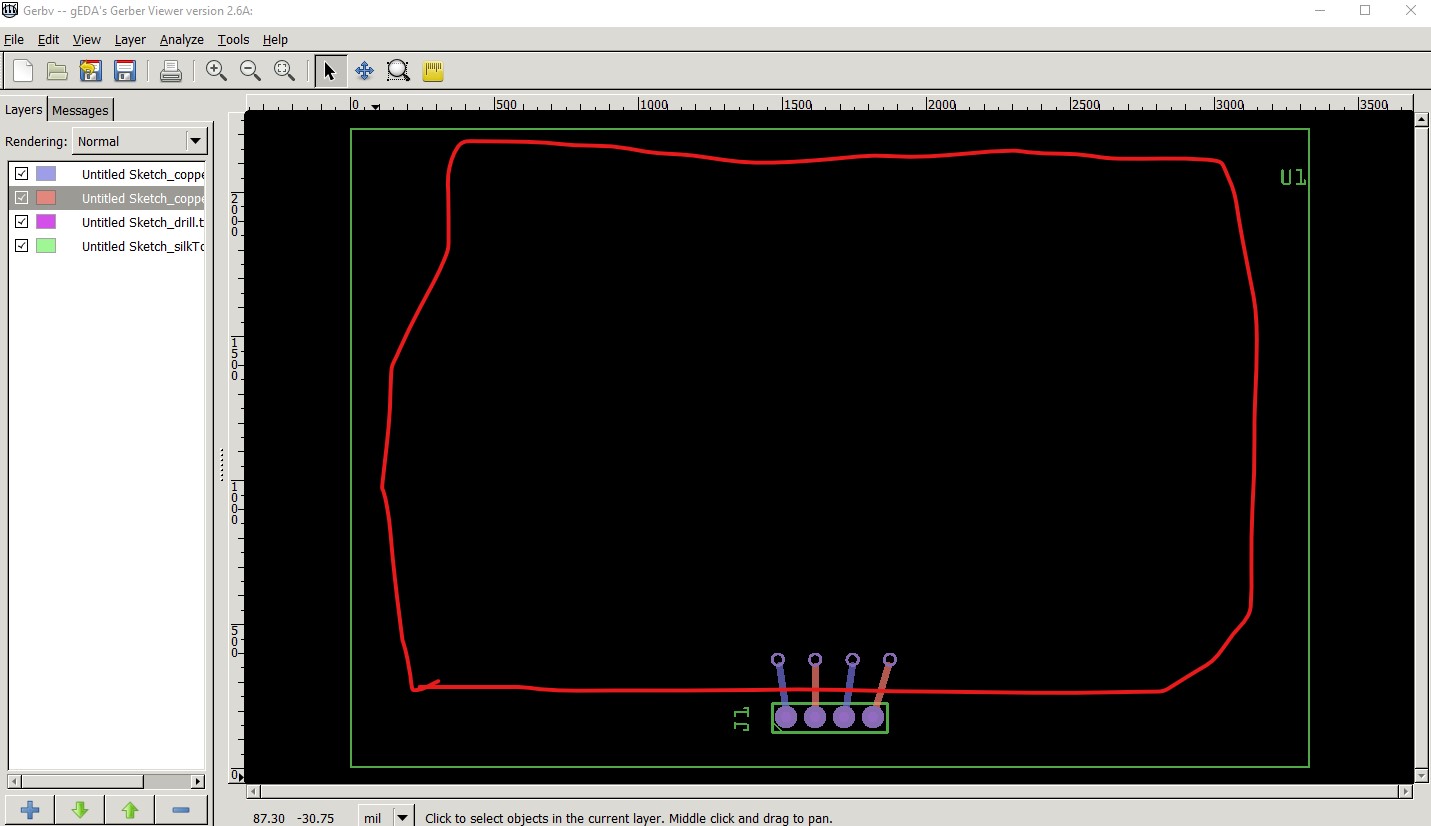
except I forgot the ellipses so we don’t get holes for the pads in this one we will have to see in the fixed version. This is the gerber output displayed by gerbv. Note there is no silkscreen rectangle and no drill holes (if there were there would be purple circles in the center of the pads)
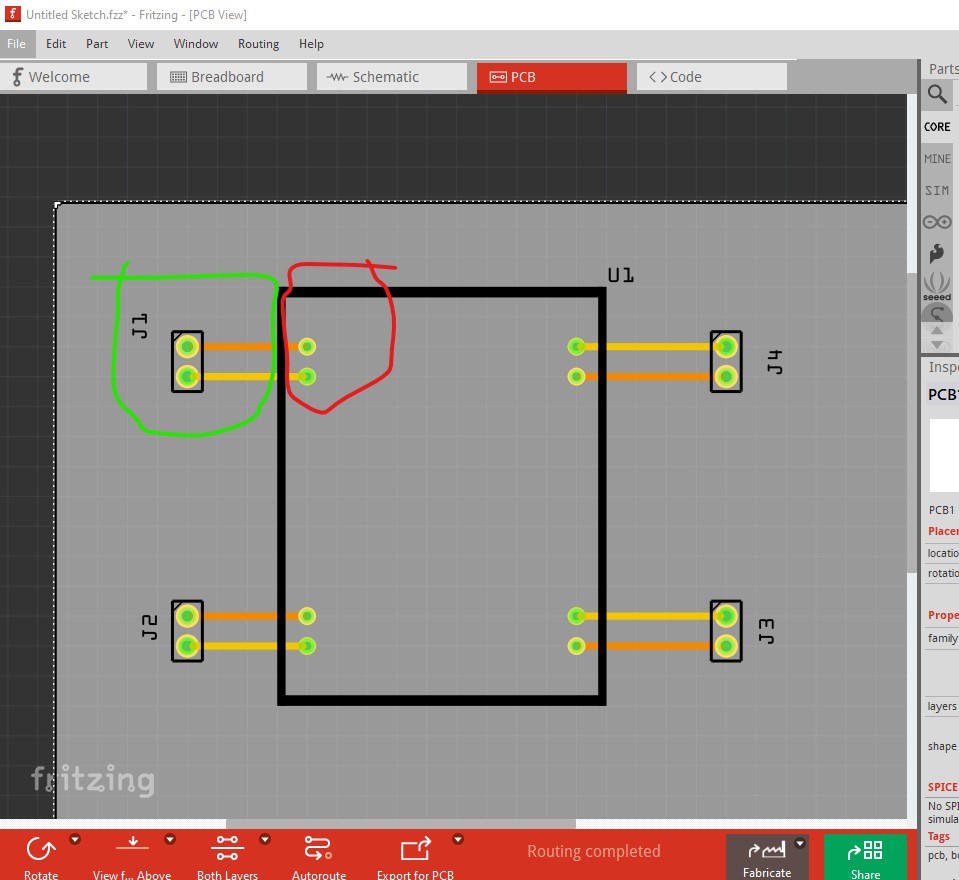
now I will repeat this with the fixed part which should show us more. In pcb we have a silkscreen outline and the pads over the circles in the copper layers.
export this as gerbers and we should see improvements. Indeed we have a correct drill file, the holes are not as bad as I though they are around 0.030in (the 0.029730 number below) from the gerber drill.txt file the 0.038 number above it is the headers.
; NON-PLATED HOLES START AT T1
; THROUGH (PLATED) HOLES START AT T100
M48
INCH
T100C0.038000
T101C0.029730
%
T100
X015555Y002333
X016555Y002333
X018555Y002333
X017555Y002333
T101
X016258Y005333
X018852Y005333
X014960Y005333
X017555Y005333
T00
M30
and the gerber output looks much better, it has the silkscreen outline, the pads on the copper and the holes
here I suppressed coppertop to make the hole more visible and zoomed in so we can see the paths rendered in copper and the holes
all of this is in the part
PWM Dimmer 5V-30V 5A 150W-fixed.fzpz (36.7 KB)
Peter