Did not faced this when I was using version 0.9.4 but now running version 0.9.6
I have a wire overlap problem.
After finishing a pcb design I plotted an Etchable PCB and noticed for the first time wire overlaps when the wire is connected to a hole:
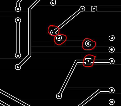
Some holes are not “open” due to the round wire end.
Same when plotting and Etchable SVG, but when I plot Extended Gerber I cannot detect this.
Increasing copper around a hole did not solve this problem. Used the same wire width all the time both in version 0.9.4 and 0.9.6
Running PCLinuxOS as my O.S.
Can someone explain what I am now doing wrong with respect to version 0.9.4.
Thanks, Joe.
While it doesn’t particularly help, something looks to have changed between 0.9.3 and 0.9.8 in terms of pdf export. This is the same test sketch rendered as a pdf first by 0.9.3:
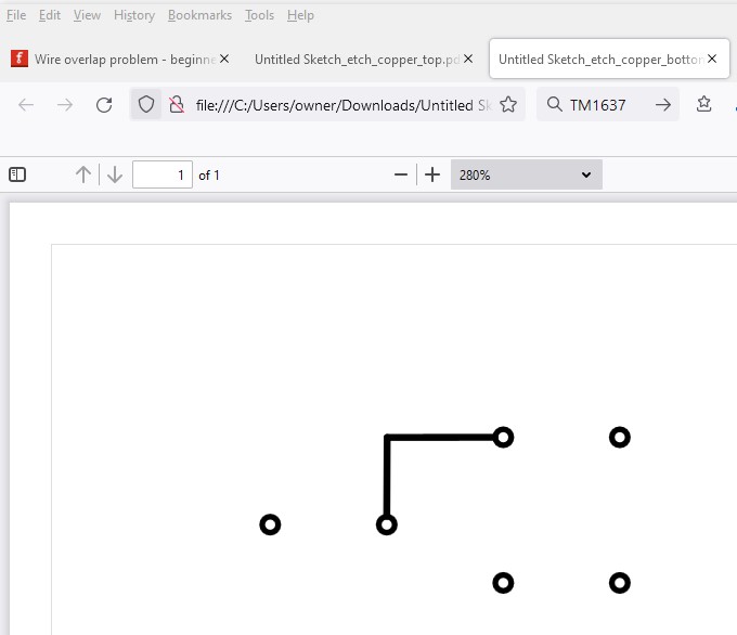
where the hole is unimpeded. Then on 0.9.8 which has the end of the pad sticking out in to the hole:

The only thing I could suggest is filing a bug report against 0.9.8 on github as it appears a change has had an undesired effect on the image export code (first check to see if this is already reported though!) The workaround is likely to be continuing to use 0.9.3 or 0.9.4 if they are working until this gets fixed. The disadvantage is that there are a bunch of fixes to the export code in both 0.9.6 and 0.9.8 but if you aren’t having problems with paths not being fully rendered in the images that may not matter to you.
edit:
it looks to be reported here:
so adding a comment to this issue would be the best bet I expect.
Peter
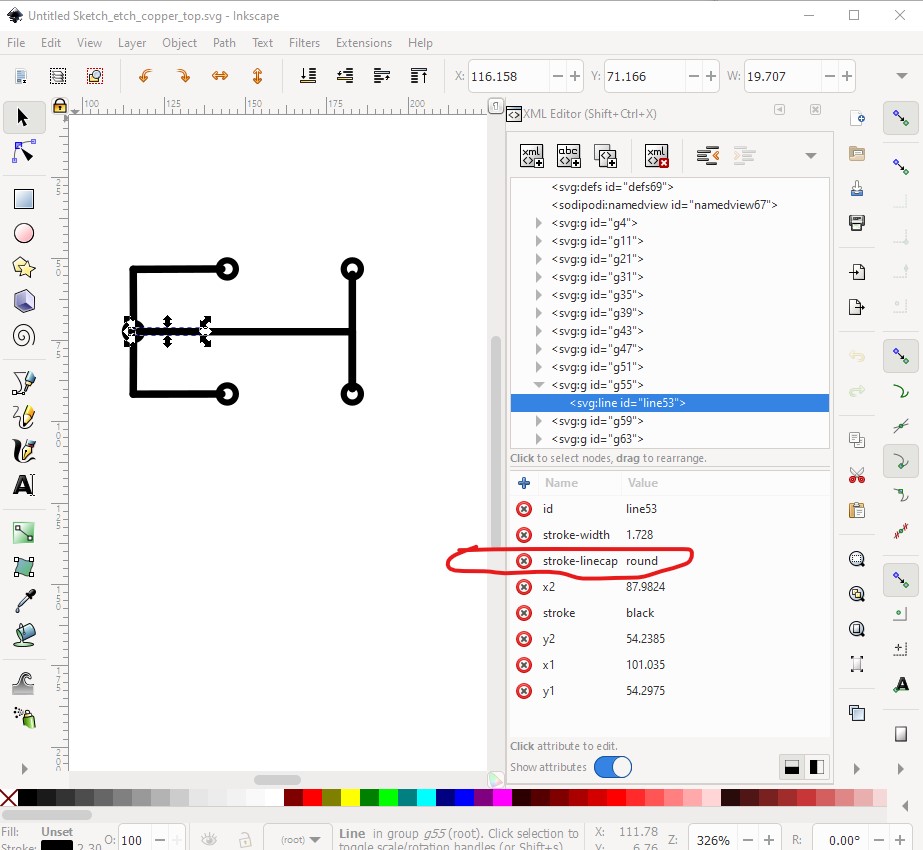
WIth the expected overlap between the wire and the pad, I can not be sure, but it looks like the difference is the newer version uses rounded ends on the wire, while the older version used square ends. Might be able to confirm that, if the svg export has the same symptoms.
Good thought, but looks not correct. It appears to be a lack of offset on the end point of the line in 0.9.8 as both have linecap=round:
0.9.8:
0.9.3b

If I recall correctly there was a fix for this in 0.9.6 that corrected the calculation but it looks like it needs to be offset (and probably thus shortened a bit too) to be correct.
edit:
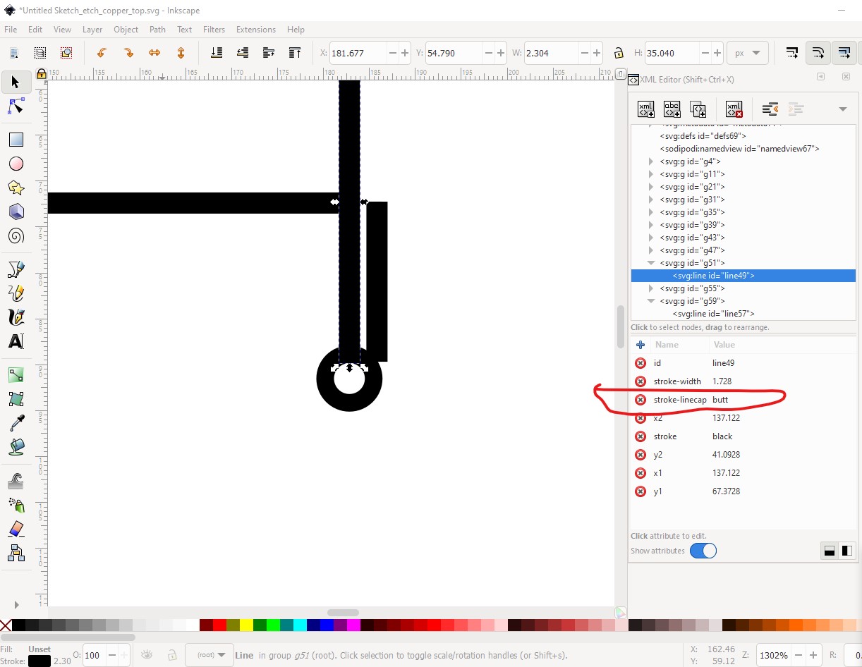
However an easy fix may be changing linecap=round to linecap=butt as long as it doesn’t break something else:
0.9.8 with linecap set to butt on 2 lines (and one line moved to get at the one under it!)
Peter
Thanks for all your comments but it still leaves me puzzled:
At this moment I am using version 0.9.6 and are running into this problem.
Did NOT have this when using version 0.9.4.
To see if I am running into this problem also when I am using an already realized PCB
I took that design (made with version 0.9.4) and ran this again using version 0.9.6.
And now I see these wire overlap problems also!
And as I have understood things correctly version 0.9.8 suffers that same problem?
So what can I do? It seems that there is no work around available?
My guess is there is a fix in 0.9.6 that causes this problem (and thus it continues in 0.9.8.) Thus the issue occurs when 0.9.6 renders older sketches as well. The only current work around would be go back to 0.9.4 (which unfortunately doesn’t appear on the historic downloads page! so I hope you saved a copy, in which case I would fall back to 0.9.3b which is available on the older downloads page) until a fix can be made and hope you don’t run in to any of the path render bugs fixed by 0.9.6 and 0.9.8.
Peter
Peter, what I do not understand is that it seems that only I have this problem and no other user of Fritzing? Asking this because my design is a very straightforward one with nothing fancy tricks in the pcb layout which could suddenly show this overlap problem.
Joe.
Everyone using 0.9.6 or 0.9.8 has this problem. It looks like a change made in 0.9.6 changed how the pads are rendered and wasn’t noticed. Now if you render an older sketch in 0.9.6 or 0.9.8 this problem will appear when it didn’t in 0.9.4 and earlier.
Peter
Well, before I posted my problem I DID take a look in the “Bugs” category but could not
find something similar to my problem, at not a recent one. But of course I could have overlooked this.
Joe.
I think this is part of the Thick traces overlap holes issue from 2015. Part of this was I believe fixed in 0.9.6 and the fix appears to have caused this new problem. They look to be aware that it still has issues but I will add this to the comments in the issue in a bit.
Peter
O.K. But I have to ask the software people of PCLinuxOS if they are willing to re-install version 0.9.4 in our repository so I can let Aisler make my pcb’s, otherwise I have to wait for a fix.
Joe.
While I’m not familiar with PCLinuxOS specifically, usually the app-get type application loader can load older versions of software (if the older version is in the repository!) by just requesting it do so. So if 0.9.4 used to be there (or 0.9.3b which should also work) one of them should do the job.
Peter
I don’t think that this is an issue for the manufacturer. They will drill a hole and the copper on the hole will be removed. Contact your manufacturer if you want to be sure.
This is only a problem if you etch the pcb at home and use a manual drilling machine as the tip of the drill bit will not self-align at the center of the pad/via.
I had missed the Aisler in this. As far as I know Aisler uses the gerber output which is not affected by this bug. It generates a drill file that specifies the x/y position of the holes which are drilled before the board is etched (so plating through will work.) As @fai noted the bug only affects you if you are home etching (which I had assumed is what you were doing.)
Peter
Thanks fai, I will write a message to Filix (from Aisler) if there could be any problem concerning this bug when they manufactor my pcb design.
O.K. Peter thanks for the explanation. As I wrote to fai, I will contact Felix about this problem before I will get things manufactured by Aisler.
IIRC, there was also an issue where thin wires would be disconnected from the copper ring (which would result in a broken circuit board).
A somewhat working solution was to start the wire closer to the hole. Since the copper will be removed when drilling the hole, this is usually not a problem.
A clean implementation would of course get this right, e.g. by cutting the hole from the wire end during PDF export. But right now it is a lower priority, since it seems more like a cosmetic issue.
Thanks Kjell for your explanation. You wrote:
“But right now it is a lower priority, since it seems more like a cosmetic issue.”
OK., but I think it is wise to wait for the comments of Felix (from Aisler) until I order a PCB from them?
Did sent him an email yesterday but did not(yet) receive a response from him.
When you upload the fzz to Aisler, does their preview show the effect?
“When you upload the fzz to Aisler, does their preview show the effect?”
Good idea, will do that and let you know the result.
Joe.