It seems that nothing is wrong here:
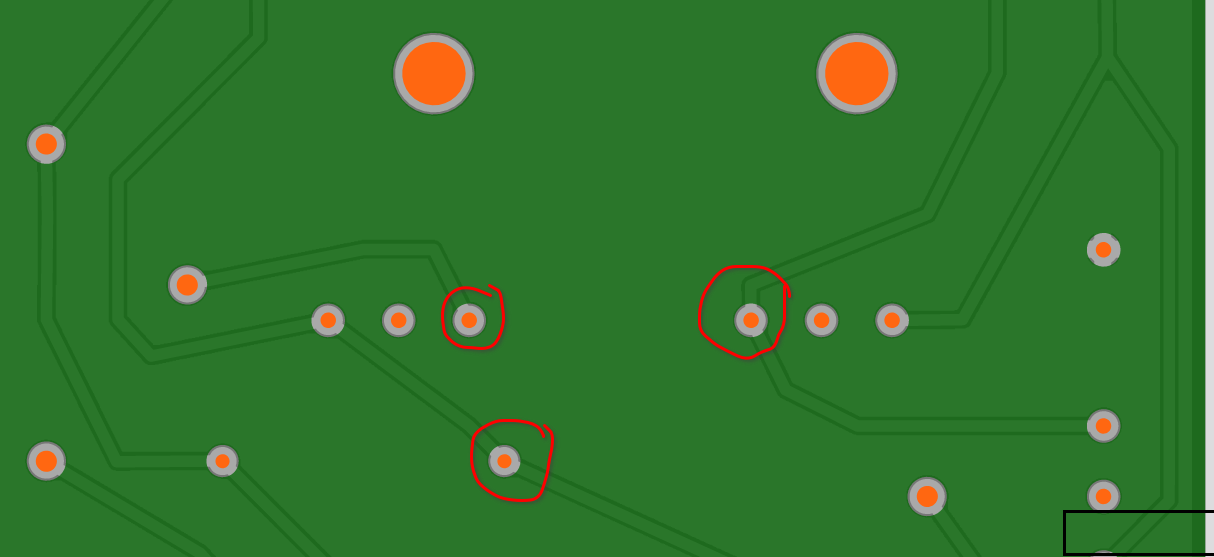
Looks that all holes are open and the wires are correctly connected to the holes.
But are you all sharing my opinion?
It seems that nothing is wrong here:
Looks that all holes are open and the wires are correctly connected to the holes.
But are you all sharing my opinion?
I do. The code that produces the gerbers (likely what is used here) is different than the code that creates the etchable images. The gerber code does not have this error-.
Peter
So it is perfectly safe to let Aisler fabricate my pcb design and those pdf and svg etchable layouts just have some cosmetic issues as Kjell wrote.
I hope that Felix will respond soon on my email to him.
Because I still not have received any response from Felix (  ), I decided to take the risk and ordered the manufacturing of my PCB.
Keep you informed.
As promised here an update about this subject.
Although Felix did not took the effort to give a response to my email to him ( ) , I took the risk and ordered a new PCB which shows that overlap on the PDF drawing. Received the PCB’s this afternoon and nothing is wrong with it.
Again in impeccable fabrication!