Is there anyone out here on the Forum who already made PCB layouts for vacuum tube sockets?
Looked into “core parts” and “connection” but could not find a clue there.
I know I can spent time to make them myself but if someone has already done this…….
I am looking for the 9 pins Noval socket and the 7 pins miniature socket.
Then I can add these to my component library.
A google search for “fritzing part 9 pins Noval socket” turns up someone looking for one in 2018, but no part, so I would guess there isn’t one yet. If you need help making the part, feel free to post.
edit:
A late thought: someone a couple of years ago made Nixie tube parts, they should have a similar (but probably not exact, likely 11 pins I think) layout. Actually 14 pins when I searched for it:
Great! Thanks for the responses. Will have a look into nixies and perhaps I will try to design something myself using this nixie stuff.
Much appreciated!
Joe,
I’m looking for the tube socket layouts also. A member from different forum sent the attached file of tube socket footprints from DesignSpark, but I’ve not been able to change them to .fzpz format. I’ll attach the link, as well as a jpeg screen shot of a properly scaled 9 pin socket I did freehand. If I could group that layout and title it as new part, or copy group and paste, that would be ok too. I just don’t want to have to freehand 5 more of those- call me lazy- lol!
While I’m not Joe, I probably can make you a part if you have more information. The forum appears to have done something odd to your url (I suspect the … shouldn’t be in the middle of it) and it tells me file not found:
and a search on the rs site doesn’t find a Tubes2.zip (although it may be later in the hundreds of hits.) I can probably use the jpeg above to do a start at a part, but what I need is the diameter of all the holes. To make a part, you basically create a svg file of the pads so something with the x/y coords of each pin and the hole diameter (like a pcb footprint for an IC) is what is needed. I’ll have a bash at the jpg and see what I can do.
the pin holes are 0.07in diameter and the center hole is 0.2in diameter. If you unzip the above .fzpz file, you will get a .fzp file and 3 svg files.
svg.pcb.9-pin-tube-socket_1_pcb.svg
is the pcb file where you can change the sizes of holes. It may be easiest to specify the hole size you need and let me change it. Breadboard and schematic are a black and white copy of pcb at present.
Many, many thanks guys for all the work you made. Much appreciated !
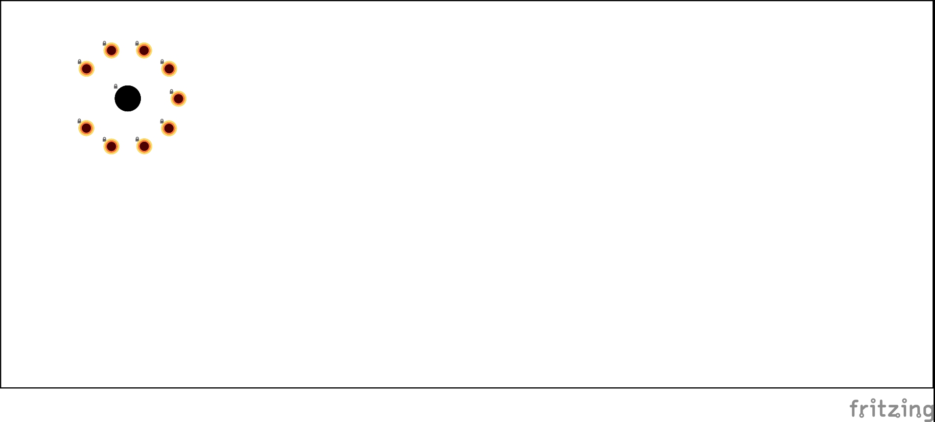
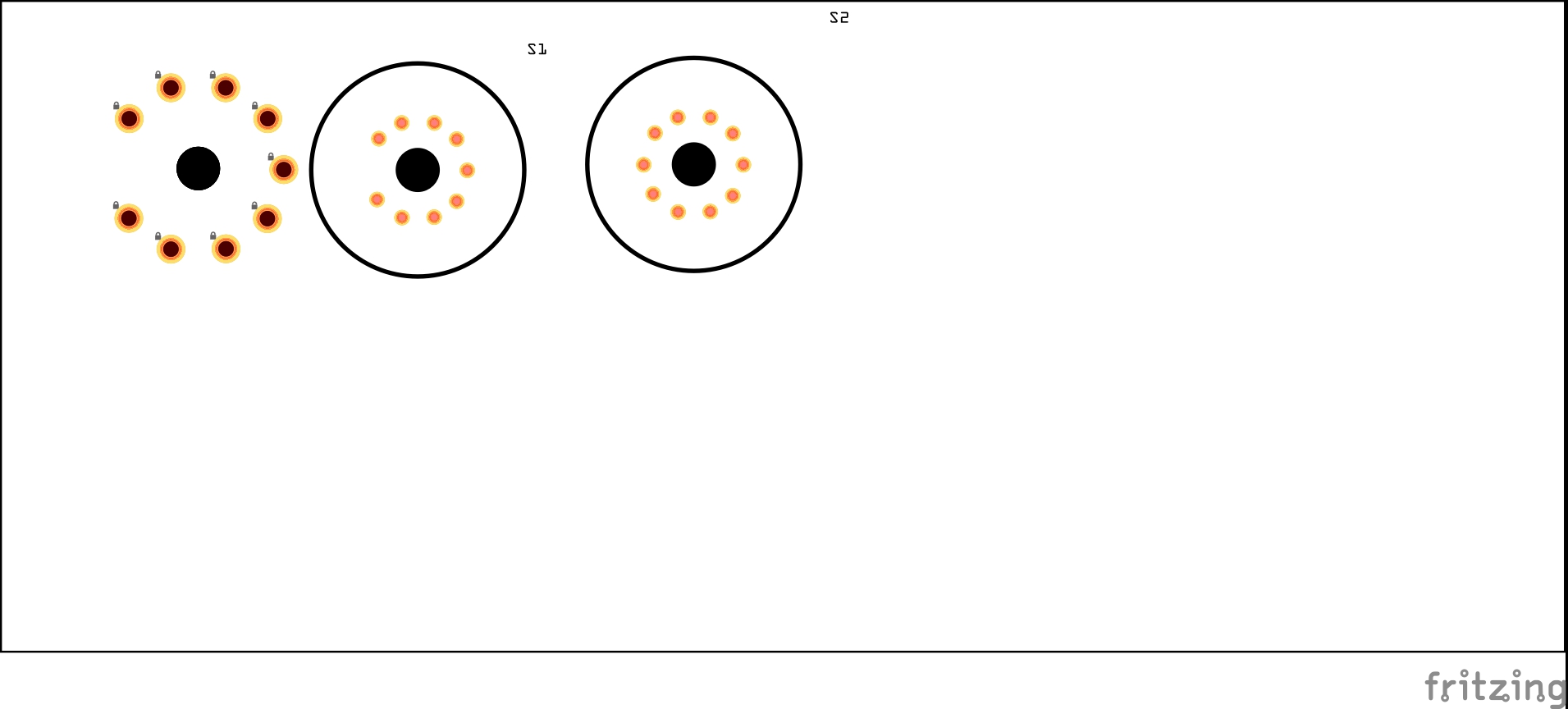
In the meantime I made a model myself, a 9 pins Noval socket, but without a centre hole and used that in one of my pcb’s. In stead of 9, I made 10 pins ( = 10 holes) so I am able to leave one hole out where that is suitable in the pcb layout (then I do not have to do a rotation).
But I still did not manage to make it a library model because I do not have the foggiest
idea how to do that.
Yes, there is something odd with that link oemcar provided.
But Peter did give that .fzpz file. Wiil see how I handle this one, will let you know as soon as possible. Again many thanks for the efforts!
Joe.
Peter,
Jolly Good Show!
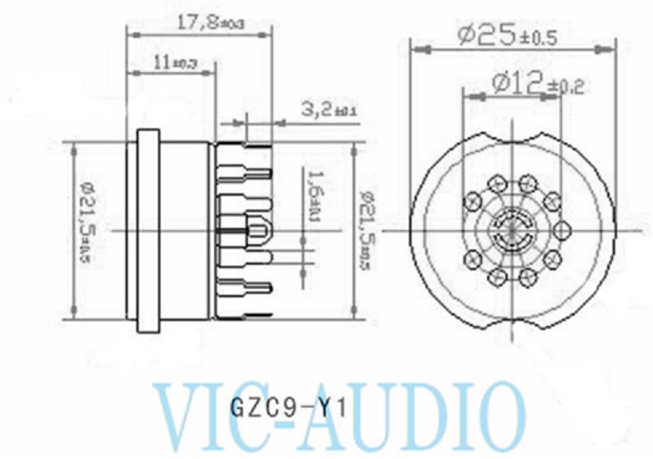
Dont know how you got dimensional info from my jpeg- but I’ll take it. You are correct the hole size is .070". Copper pads were .025", but I’ve changed that to .030". The group of 9 is on a .400" radius. Center hole is .200". Lets try again on the link- May have not grabbed all of it first time- sorry.
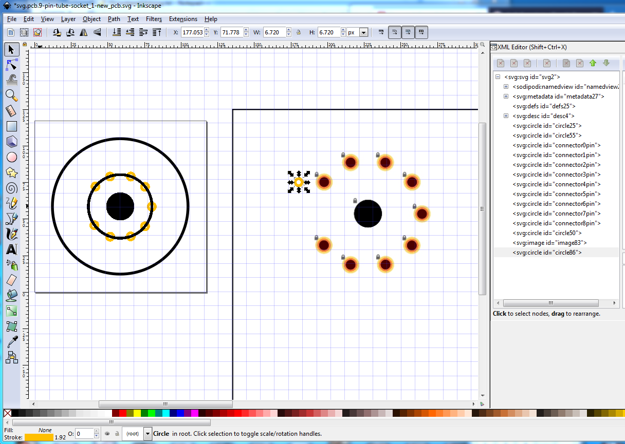
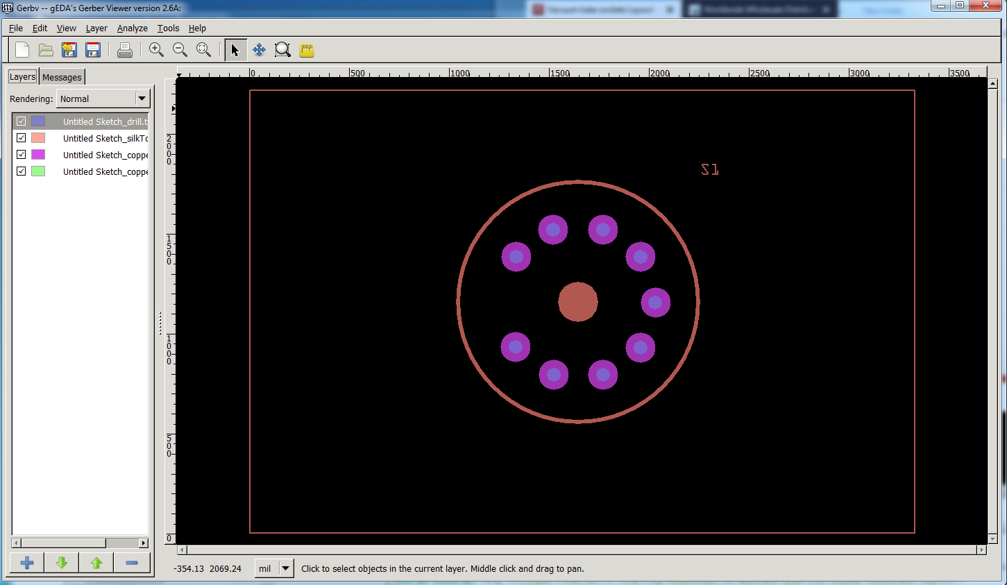
Good suggestion on the hole, I’ve moved it to silkscreen so you can drag a hole over it if you need the center hole. The original svg came from downloading your jpg and importing it in to Inkscape via File->import which gave me this (without the current socket on the left):
I then created a pad (selected in the image) and moved it over the pad in the jpeg, then resized it til the internal hole appeared to match. It looks like something in the conversion wasn’t quite right because the pin radius is way too large (although the center pin was correct.) So in this svg I have set the pads to be 0.030in (in Inkscape that means the diameter is 0.070in and the stroke-width is 20 because hole size = dia - (2 * stroke-width). I managed to get the zip file OK this time, but I don’t have anything that will read the files (presumably their tool does) so instead I used the drawing above to move the pads on to a 12mm (.472in) radius circle. They may need to move a bit in x and y to be properly positioned as the current position is from the jpeg. A trick for changing pad size in Inkscape is to change the diameter with the tool bar (which also undesirably changes the position of the center of the pad), then note the new radius value from xml editor. Now undo the diameter change via undo and instead change to the new radius in xml editor and the pad will change size maintaining its position. Here is a copy of the svg (ungrouped) with the 12mm circle still present:
good, the forum is feeling happy today and up loaded the svg. It did set the size to 1px by 1px, but changing that to 1000 * 1000
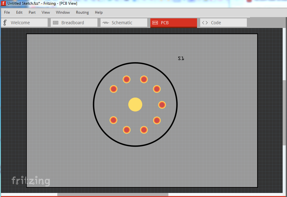
lets it render and thus should be downloadable by clicking on it. Here is an updated part (I left breadboard and schematic as is with the wrong sizes for now) with the above changes in and grouped and the construction 12mm circle deleted:
Great that, at last, there is a “library model” for the 9 pins Noval socket. But I think for
pcb use there is no need for the centre hole, just make a simple reference cross. And, as I have suggested before, make that model “10” pins to have freedom of leaving out one hole to get rid of rotating the model in order to let it fit in your pcb layout. But that is my humble opinion.
If you look at this link from the (Dutch version, just copy/paste into your web browser to see what I mean)) Conrad supplier:
This socket is which I am using now on my pcb layouts.
In the latest part the center hole is only on the silkscreen. If you want the center hole you need to drag the hole in from core parts and set its size to match the size of the hole.
I can do such a svg without problem, but that makes it easy to insert the socket in the wrong place as it will fit in any orientation. With the correct 9 pins it will only fit in the correct position. As well if you want to make real tubes (as opposed to only a pcb footprint) the pin numbers matter in breadboard and schematic. Here is a 10 pin part with breadboard and schematic updated as well. Note one of you needs to print out the footprint at 1:1 scale and check that a real socket actually matches the footprint (I don’t have a socket to try.)
Peter,
Thanks again for your speedy assistance-
Looks to me like the layout may be 9 holes on diameter instead of radius? Pins look to be about half size too…Is there a scaling entry I’m not aware of?
Attached jpeg comparing two imported .fzpz’s supplied V my original layout is below.
Thanks again,
Jim
I was going by the mechanical drawing a few posts up which shows the pins to be on 12mm diameter circle, so it should in fact be the size of the ones from the jpg? I assumed I had a scaling problem on the jpeg import. I’ll move them back to the jpeg positions and see if that is better.
edit:
see if this one works better. This is the original spacing from the jpeg with the pads set to a 0.03in hole and the center hole moved in to silkscreen.
edit
replaced by the correct part at the end.
I think the mechanical drawing above is wrong, the 12mm diameter for the pins doesn’t match the pins on the left which look to be about 18mm diameter. So I guess see if this one does better (indicating the jpeg was it fact correct!)
Peter,
I believe you are correct in 12mm spacing reference was to points in the socket. I believe points at the PCB were shifted outward by design.
When I try to import your above file- an error msg comes up that a ‘9 pin tube socket already exists’. Renaming the file after download doesn’t help. Perhaps renaming the file name at your end will preserve its originality? Something simple like “2”? So import doesn’t have anything recognizable in title from previous import?
Thoughts?
Jim
You likely need to delete the current part (I didn’t change the moduleId which is what it is complaining about) and then exit and restart Fritzing. In theory the source code thinks that delete removes the part entirely, in practice I often have to exit Fritzing after doing a delete to be able to reload a part with the same moduleId. Finding and fixing that bug is on my list, but not done yet.
Yes, I see from the mechanical drawing the pins are 1.6mm (0.06299in) so the holes should be 0.07 (as the original jpg was!) not the 0.03 I picked up from the discussion somewhere. I’ll fix that up now.
it is already deleted, the circle is only in silkscreen, it won’t drill a hole. If the user wants the center hole they can drag the hole from core parts and place it over the circle in silkscreen to drill the hole.
That will work but I think the granularity is only 45 degrees minimum for rotate and that may not be fine enough in some cases. Two parts (one with 10 pins) isn’t a problem, although I’d advise using the 9 pin version to make part placement easier. OK third time lucky hopefully. Here is a corrected part, the stroke-width on the pads is 40thou (instead of the usual 20thou) and the hole size is 0.07in which should give a little room for pin variation.
edit:
replaced by the correct part at the end.
gerber drill.txt file
; NON-PLATED HOLES START AT T1
; THROUGH (PLATED) HOLES START AT T100
M48
INCH
T100C0.070000
%
T100
X013336Y009347
X019576Y013836
X013357Y013836
X015243Y007940
X015222Y015222
X020326Y011545
X017722Y015222
X019586Y009305
X017722Y007940
T00
M30
Hopefully I got my head around all of it this time , I should adjust the breadboard and pcb svgs to match pcb, but it will work fine as is, the connectors are all there and thats all Fritzing cares about,
I think after reading all those responses that I am lost here. After downloading and extracting those .fzpz files, I exepected a .fzz file to work with and after a 1:1 printout
check it against a hardware socket if things are correct. But I failed, sorry.
There are no .fzz files to open with fritzing or do I completely misunderstand somthing here?
You must remember that I am still a beginner.