
I just included a picture of the sim900 shield, can someone pleaseeeee make a model of this in fritzing? I need this ASAP for my school project
I just included a picture of the sim900 shield, can someone pleaseeeee make a model of this in fritzing? I need this ASAP for my school project
There isn’t enough information here to make a part (and there doesn’t appear to be a part in a google search for “fritzing part sim900 module”.) To make a part we would need a mechanical drawing with the dimensions of the board and a listing of the labels (at a minimum) and preferably the use of all the pins. I can’t immediately see either of those in a google search for sim900 module. So pointers to web sites that have that information would be the next step.
Peter
Hello, I am searching too. But cannot find any location for download.
But I have some documentations like PCB and SCM
(ZIP-File - click “view raw” for download)
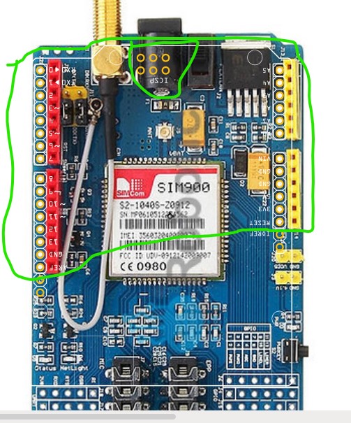
Only some Pins are connected to Arduino
Digital Pin 0 – RX optional einstellbar per Jumper
Digital Pin 1 – TX opttional einstellbar per Jumper
Digital Pin 7 – per SoftSerial (Default) RX
Digital Pin 8 – per SoftSerial (Default) TX
Digital Pin 9 – Power On/Off (1 Sekunde HIGH)
5V – über Schiebeschalter
GND – GND
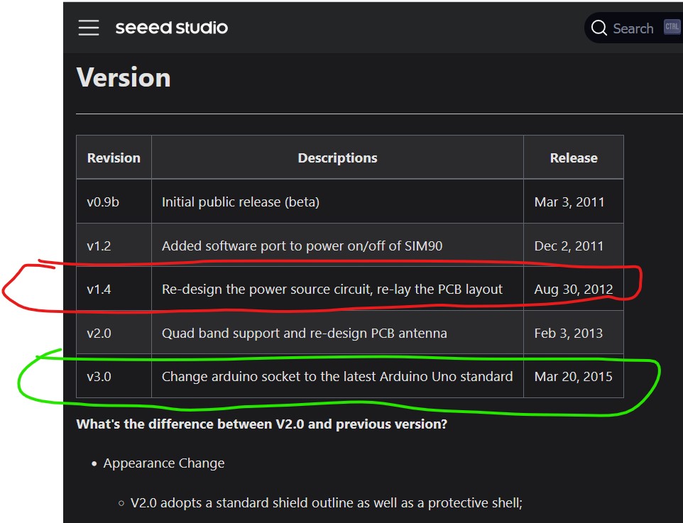
The question is what version do you want? The zip file is for version 1.4, but the latest version appears to be V3.0 with 1.4 being two versions back.
Peter
I don’t know the version. The documents I found are mixed.
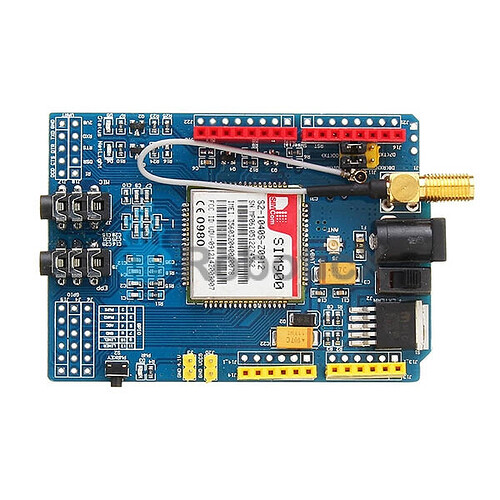
This photo is exactly my version I have
I think the version doesn’t matter because only some pins are used. These pins are always the same.
This appears to be V1.0 think a part for V3 (the current version being sold) makes the most sense so I’ll make one of those.
Peter
This part should do what you want. Note the 4 active wires on the audio jack are all on the top (the numbers in the pin description match the connector numbers on the jack) and may not be in the correct physical position. There are also some new connectors added in V3 which likely aren’t in the older versions but it should still do what you want.
seeed-gprs-shield-v3.0.fzpz (24.7 KB)
Peter
Hello and thank you.
This part only fits the pins to the Arduino. Only 7 pins are used. The picture is wrong and would be totally misleading in craft instructions where I want to use it. I think that this shield doesn’t come from “seeedstudio”, but is a clone that is produced somewhere else. You can find it on Amazon, Ebay, AliExpress and many other retailers. And various Chinese manufacturers are named. In addition to the 7 relevant pins for the Arduino, the shield also has a lot of pins for other purposes that could also be interesting. These pins above and below the phone jacks should be present as connectable pins on a “frizzing” layout. Names are probably not necessary. Anyone who needs such special pins will find the right ones themselves. The main thing is that you can connect a line if necessary.
As noted earlier, the picture on the right is the version 1.4 version of the board. If that is what you need I can make one tomorrow (I expect someone else will want the latest version so it won’t go to waste!)
Peter
Hi,
the picture on the right is a shield which is not from Seeed Studio and it is not V1.4. There is no such Version 1.4 in the internet. Seeed Studio only has up to V1.3.
My Shield, on the right of the picture, has no version number. It is sold worldwide with no Version and it is not full compatible with the layout with the other shields from Seeed Studio.
Examples
https:/ x /www.roboter-bausatz.de/p/sim900-quad-band-gsm-gprs-shield-fuer-arduino
(Last link broken because of limit to post max. 2 links)
But this all does not matter. The mechanical layout is typically Arduino Uno.
Only 7 Pins are used from the shield and have to be coennectable.
D0, D1, D7, D8, D9, 5V and GND
Additionally the shield has some rows of pins of interest on it which should be available to connect in frizzing for special purpose.
I never worked with the part-editor. I think you can use a prototype-layout or something else, place the picture on it fitting to the pins and define the pins which are to be connected in the schematic.
Best regards Wolfgang
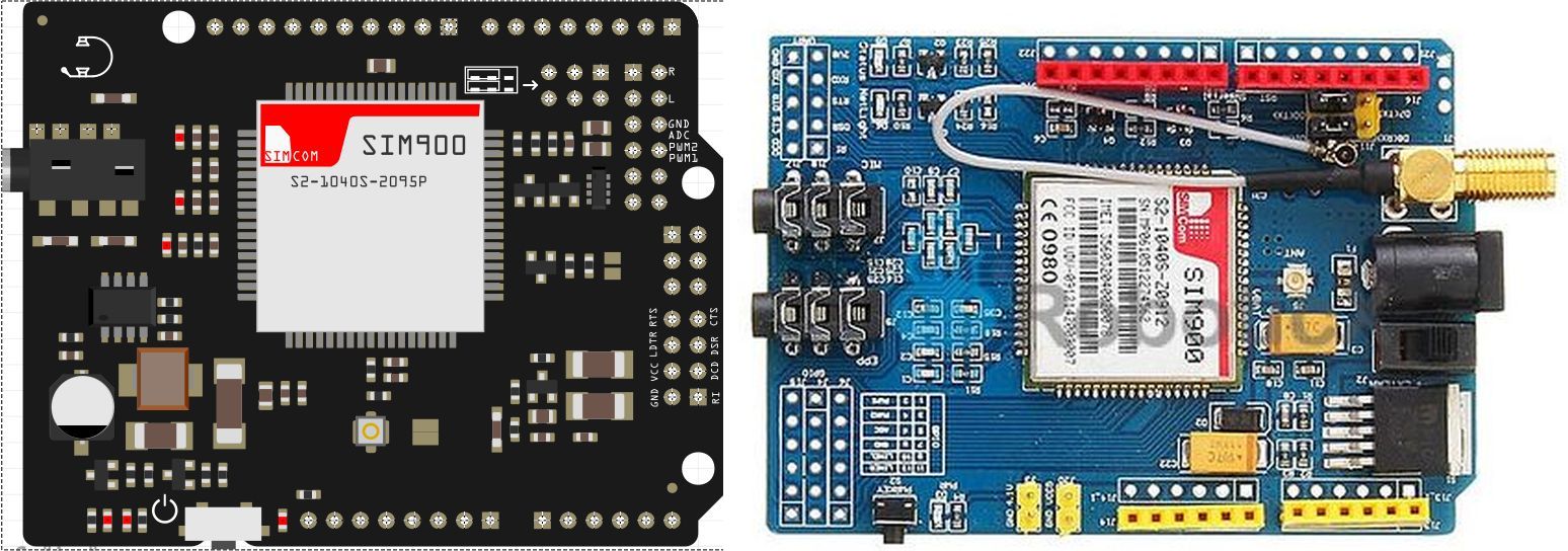
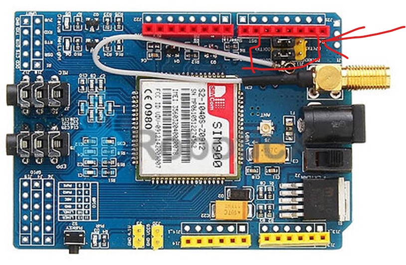
I need an image of the exact board you want like this one but with better detail of what the connectors do (I need to be able to read the printing on the connectors to be able to figure out what they do, and reproduce the labeling in the part)
and preferably flat like this one so I can place the connectors using the image. That may be hard to find as they don’t appear to like posting detailed images (I expect to block reverse engineering!) most of the ones I see are poor resolution. This is the Seeed part that I am referring to:
it lists (in the version section) that this is version 1.4, there are eagle files for the board available which makes layout easier. It may or may not match what you have though. The part that I made is for V3.0 which appears to be the latest released in 2015. At present I don’t have enough information to make a board.
Peter
Maybe this is the pic : https://m.media-amazon.com/images/I/510-b+O9QSL.jpg
Hello Peter,
The Seeed part is not the same which are actually sold in the net. I think this are clones
The eagle-files are not 100% the layout and the schematic from this board!
picture 2 comes later
picture 3 comes later
because of forumsoftware blocks more than 1 picture at time
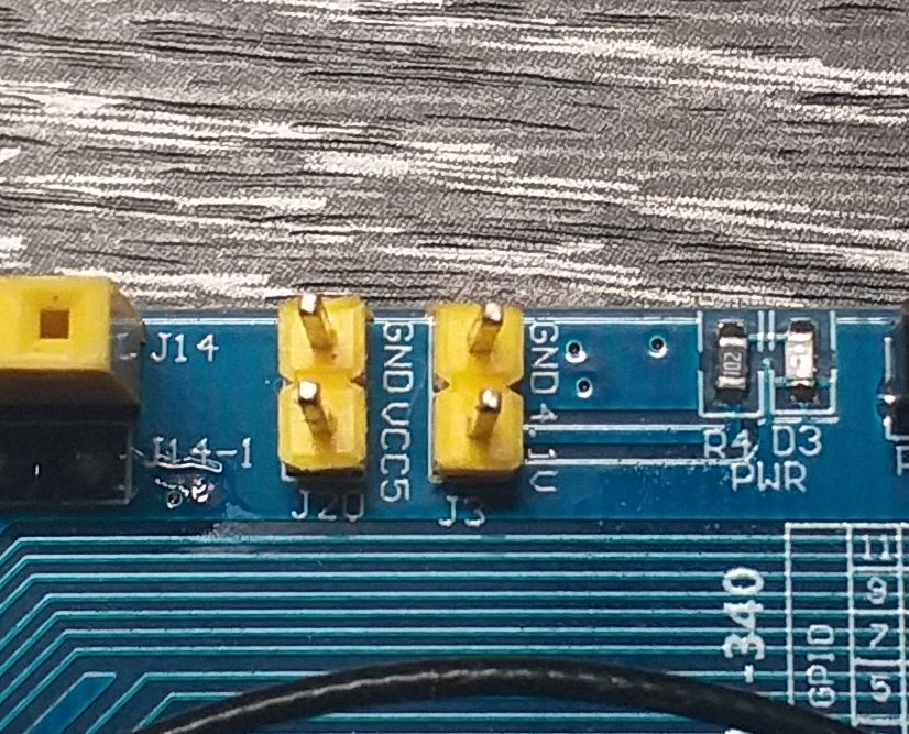
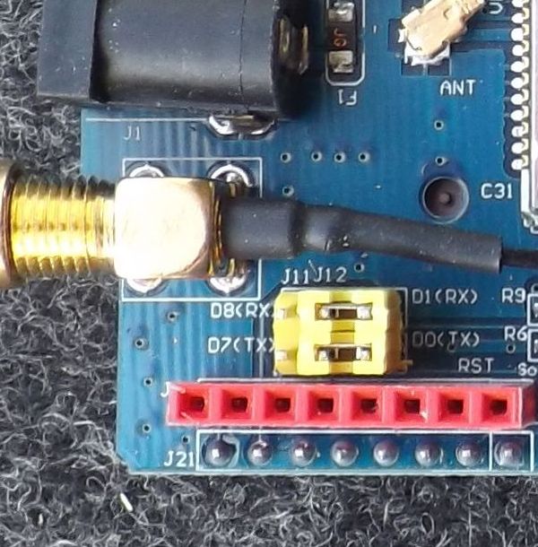
The last picture for example shows a difference to the Eagle-files. We have 2 Jumpers and the Seeed-parts have only one.
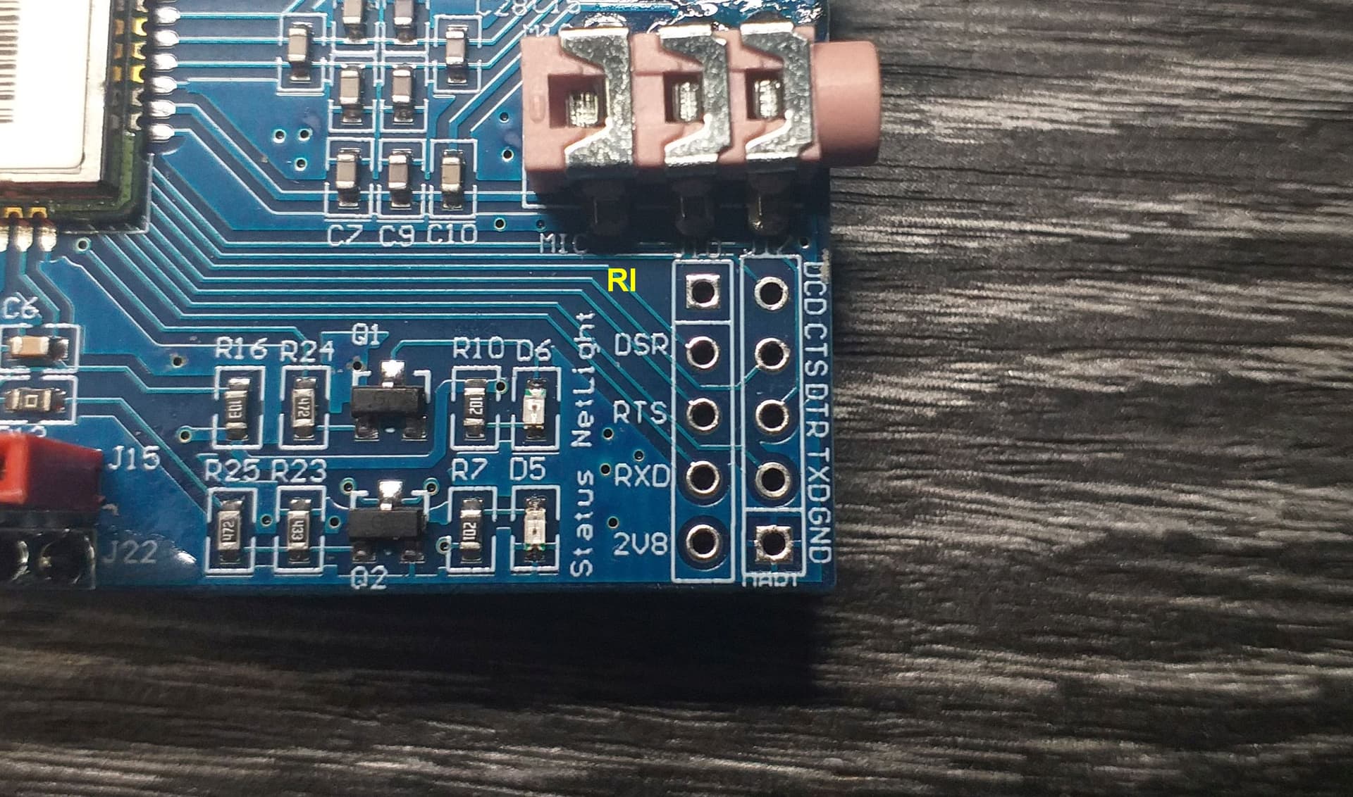
The yellow “RI” is the Ring-Signal. Connected but not named.
I think the first photo of your board is the best I’m going to get, one last set of jumpers (unless I missed them) though
They look to be jumpers for something likely uart settings I expect. With that we should be good to go I think.
edit
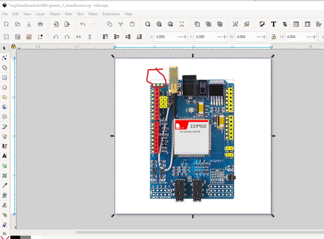
OK I think I have it now. I imported your jpeg in to Inkscape then copies in the pcb svg from a UNO and scaled and rotated the jpeg til the pins matched the layout of the UNO. That should give me enough to make a part from.
The gold circles are the pcb image of the UNO and they match (with the jpeg scaled and rotated) the pads on the board which in turn sets the size of the board and the placement of the components. Since we lnow the UNO PCB is correct if the jpaeg matches it too should be correct. I’ll proceed from there, I don’t need to know what the last set of jumpers do until I’m setting the .fzp file which is at the end of this process.
edit
OK breadboard is mostly done. I still need to create red female headers and add pads and text. I also found another mystery connector that would be good to add if you know what it does (circled in red in this image.)
this image is with the base under the jpg image the real part will look like this (when completed!)
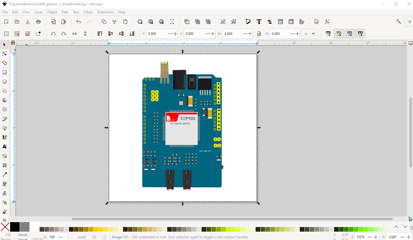
edit2
OK here is a part that should do what you want. Note the 3 connectors on the top have a ? label as I don’t know what they do. If you know their names it is easy enough to add them. PCB view is suppressed as not useful (only breadboard and schematic are active.)
edit3:
Sep 27 2023
replaced the original part with a corrected one (all pin labels), if you have downloaded the part before Sep27 then please redownload it to get the updated part.
sim900-generic.fzpz (30.3 KB)
Peter
1 Like
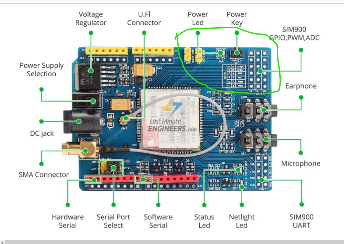
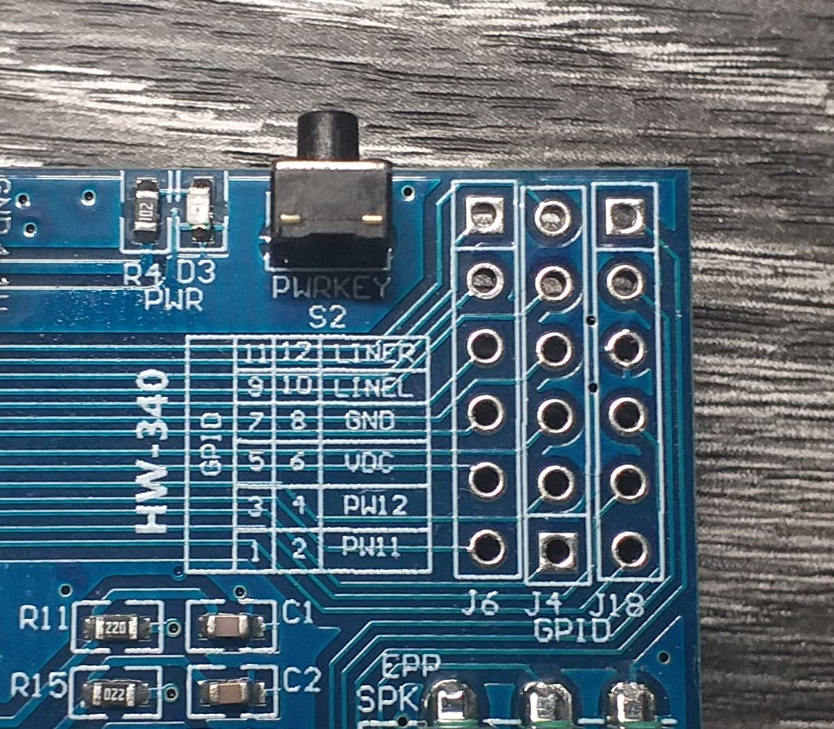
With this 2 jumpers you select software-serial (DO-D1) or hardware-serial (D7-D8)
the 2 rows of 3 pins in the top-middle are only on the UNO. Here we do not need them
The three pins in the top left are only on the commercial photos. My Board does not have them
What about the many empty pinholes near the phoneconnectors? These should be connectable pins for external use because these pins are useful signals. For example “RI” - But they don’t need names. This special people who will use it will find out which pin is which signal
Thank you very much! I will test later because I am on work.
Hello,
I tried my first experiment with the new part. It looks very good!
But the TX/RX-Pin-Names are totally scrambled
Correct is now:
36 PD8/D8/RX 37 RX serial select 38 PD1/D1/RX
33 PD7/D7/TX 34 TX serial select 35 PD0/D0/TX
I have changed it with the part editor. My first contact with this tool.
The change is correct in partview. But not in the schematic view. There are the same wrong texts at the pins like before. I find no way to change it here too.
To change schematic you need to use an svg editor such as Inkscape. To do that you need to unzip the .fzpz file which will give you a file called
svg.schematic.sim900-generic_1_schematic.svg
which looks like this in Inkscape:
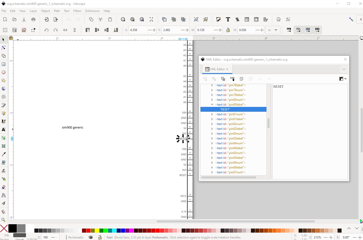
Here I have selected the RESET pin name and it is changeable in xml editor on the right. If you aren’t familiar with Inkscape it may be easier to let me make the changes (you also need to run the part through FritzingCheckPart.py to clean up some Inkscape features that are incompatible with Fritzing.) If you like instructions are here (although it is complex!) in the tutorials section of the forums:
or you can upload the .fzpz file that Parts editor made (upload is 7th icon from the left in the reply menu) and I can make the necessary changes from the fzp file. As well do you have pin names for the 3 connectors on the top of the board?
Peter
Hi,
sorry - this all is too complicated for me. I never worked with “svg” or any tools therefore.
You made the file part-file yesterday. It would be nice if you would correct these little naming-bugs and repost it in new version.
The three pin names are not on my board an in no documentation I found. They are only in the commercial selling pictures.